ICGOO在线商城 > 集成电路(IC) > 逻辑 - 缓冲器,驱动器,接收器,收发器 > SN74F125N
 Datasheet下载
- 型号: SN74F125N
- 制造商: Texas Instruments
- 库位|库存: xxxx|xxxx
- 要求:
| 数量阶梯 | 香港交货 | 国内含税 |
| +xxxx | $xxxx | ¥xxxx |
查看当月历史价格
查看今年历史价格
SN74F125N产品简介:
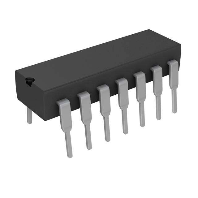
ICGOO电子元器件商城为您提供SN74F125N由Texas Instruments设计生产,在icgoo商城现货销售,并且可以通过原厂、代理商等渠道进行代购。 SN74F125N价格参考¥1.18-¥3.40。Texas InstrumentsSN74F125N封装/规格:逻辑 - 缓冲器,驱动器,接收器,收发器, Buffer, Non-Inverting 4 Element 1 Bit per Element 3-State Output 14-PDIP。您可以下载SN74F125N参考资料、Datasheet数据手册功能说明书,资料中有SN74F125N 详细功能的应用电路图电压和使用方法及教程。
SN74F125N 是由 Texas Instruments 生产的一款逻辑缓冲器,属于高速 TTL(晶体管-晶体管逻辑)系列。它主要用于信号传输和电平转换,广泛应用于数字电路设计中。以下是 SN74F125N 的一些典型应用场景:

 1. 总线驱动与隔离
   在多设备共享同一数据总线的系统中,SN74F125N 可以用于驱动总线,确保信号在长距离传输时不失真。它还可以作为隔离元件,防止多个设备同时向总线发送信号,避免信号冲突。

 2. 电平转换
   SN74F125N 可以用于将低电平信号转换为高电平信号,适用于不同电压等级的电路之间的接口。例如,在 TTL 和 CMOS 电路之间进行电平匹配时,它可以确保信号的正确传输。

 3. 信号增强
   在长距离或复杂布线环境中,信号可能会衰减或受到噪声干扰。SN74F125N 可以增强信号的驱动能力,确保信号在传输过程中保持稳定,减少误触发或信号丢失的风险。

 4. 并行数据传输
   SN74F125N 具有三态输出功能,可以用于并行数据传输中的总线控制。通过控制使能端(G),可以选择性地将数据从一个设备传输到另一个设备,而不会影响其他设备的工作状态。

 5. 时钟信号分配
   在需要多个模块同步工作的系统中,SN74F125N 可以用于分配时钟信号。它能够确保时钟信号的稳定性和一致性,避免由于信号延迟或失真导致的同步问题。

 6. I/O 扩展
   在嵌入式系统或微控制器应用中,SN74F125N 可以用于扩展 I/O 端口。通过缓冲外部输入或输出信号,它可以提高系统的可靠性和抗干扰能力。

 7. 工业控制
   在工业自动化领域,SN74F125N 常用于传感器、执行器等设备之间的信号传输。它能够承受较大的电流波动,并且具有良好的抗噪性能,适合恶劣的工业环境。

总之,SN74F125N 作为一种通用的逻辑缓冲器,广泛应用于各种数字电路中,尤其是在需要信号增强、电平转换、总线驱动等场合。它的高速特性和三态输出功能使其成为许多复杂系统中的关键组件。
| 参数 | 数值 |
| 产品目录 | 集成电路 (IC)半导体 |
| 描述 | IC BUS BUFF TRI-ST QD 14DIP缓冲器和线路驱动器 Quad Bus Buffer Gate With 3-State Outputs |
| 产品分类 | |
| 品牌 | Texas Instruments |
| 产品手册 | |
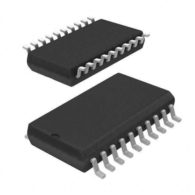
| 产品图片 |
|
| rohs | 符合RoHS无铅 / 符合限制有害物质指令(RoHS)规范要求 |
| 产品系列 | 逻辑集成电路,缓冲器和线路驱动器,Texas Instruments SN74F125N74F |
| 数据手册 | |
| 产品型号 | SN74F125N |
| 产品种类 | 缓冲器和线路驱动器 |
| 传播延迟时间 | 7.5 ns at 5 V |
| 低电平输出电流 | 64 mA |
| 供应商器件封装 | 14-PDIP |
| 元件数 | 4 |
| 其它名称 | 296-3548-5 |
| 包装 | 管件 |
| 单位重量 | 1 g |
| 商标 | Texas Instruments |
| 安装类型 | 通孔 |
| 安装风格 | Through Hole |
| 封装 | Tube |
| 封装/外壳 | 14-DIP(0.300",7.62mm) |
| 封装/箱体 | PDIP-14 |
| 工作温度 | 0°C ~ 70°C |
| 工厂包装数量 | 25 |
| 最大工作温度 | + 70 C |
| 最小工作温度 | 0 C |
| 极性 | Non-Inverting |
| 标准包装 | 25 |
| 每元件位数 | 1 |
| 每芯片的通道数量 | 4 |
| 电压-电源 | 4.5 V ~ 5.5 V |
| 电流-输出高,低 | 15mA,64mA |
| 电源电压-最大 | 5.5 V |
| 电源电压-最小 | 4.5 V |
| 电源电流 | 0.04 mA |
| 系列 | SN74F125 |
| 输入线路数量 | 4 |
| 输出类型 | 3-State |
| 输出线路数量 | 3 |
| 逻辑类型 | 缓冲器/线路驱动器,非反相 |
| 逻辑系列 | F |
| 高电平输出电流 | - 15 mA |


- 商务部:美国ITC正式对集成电路等产品启动337调查
- 曝三星4nm工艺存在良率问题 高通将骁龙8 Gen1或转产台积电
- 太阳诱电将投资9.5亿元在常州建新厂生产MLCC 预计2023年完工
- 英特尔发布欧洲新工厂建设计划 深化IDM 2.0 战略
- 台积电先进制程称霸业界 有大客户加持明年业绩稳了
- 达到5530亿美元!SIA预计今年全球半导体销售额将创下新高
- 英特尔拟将自动驾驶子公司Mobileye上市 估值或超500亿美元
- 三星加码芯片和SET,合并消费电子和移动部门,撤换高东真等 CEO
- 三星电子宣布重大人事变动 还合并消费电子和移动部门
- 海关总署:前11个月进口集成电路产品价值2.52万亿元 增长14.8%


PDF Datasheet 数据手册内容提取
SN74F125 QUADRUPLE BUS BUFFER GATE WITH 3-STATE OUTPUTS SDFS016B – JANUARY 1989 – REVISED JULY 2002 (cid:0) 3-State Outputs Drive Bus Lines or Buffer D, DB, N, OR NS PACKAGE Memory Address Registers (TOP VIEW) 1OE 1 14 VCC 1A 2 13 4OE 1Y 3 12 4A description/ordering information 2OE 4 11 4Y The SN74F125 features independent line drivers 2A 5 10 3OE with 3-state outputs. Each output is disabled when 2Y 6 9 3A the associated output-enable (OE) input is high. GND 7 8 3Y ORDERING INFORMATION ORDERABLE TOP-SIDE TA PACKAGE† PART NUMBER MARKING PDIP – N Tube SN74F125N SN74F125N Tube SN74F125D SSOOIICC – DD FF112255 0°C to 70°C Tape and reel SN74F125DR SOP – NS Tape and reel SN74F125NSR 74F125 SSOP – DB Tape and reel SN74F125DBR F125 †Package drawings, standard packing quantities, thermal data, symbolization, and PCB design guidelines are available at www.ti.com/sc/package. FUNCTION TABLE (each buffer) INPUTS OUTPUT OE A Y L H H L L L H X Z Please be aware that an important notice concerning availability, standard warranty, and use in critical applications of TexasInstruments semiconductor products and disclaimers thereto appears at the end of this data sheet. PRODUCTION DATA information is current as of publication date. Copyright 2002, Texas Instruments Incorporated Products conform to specifications per the terms of Texas Instruments standard warranty. Production processing does not necessarily include testing of all parameters. POST OFFICE BOX 655303 • DALLAS, TEXAS 75265 1
SN74F125 QUADRUPLE BUS BUFFER GATE WITH 3-STATE OUTPUTS SDFS016B – JANUARY 1989 – REVISED JULY 2002 logic diagram (positive logic) 1 1OE 2 3 1A 1Y 4 2OE 5 6 2A 2Y 10 3OE 9 8 3A 3Y 13 4OE 12 11 4A 4Y absolute maximum ratings over operating free-air temperature range (unless otherwise noted)† Supply voltage range, V . . . . . . . . . . . . . . . . . . . . . . . . . . . . . . . . . . . . . . . . . . . . . . . . . . . . . . . . . . –0.5 V to 7 V CC Input voltage range, V (see Note 1) . . . . . . . . . . . . . . . . . . . . . . . . . . . . . . . . . . . . . . . . . . . . . . . . . . –1.2 V to 7 V I Input current range . . . . . . . . . . . . . . . . . . . . . . . . . . . . . . . . . . . . . . . . . . . . . . . . . . . . . . . . . . . . . . . –30 mA to 5 mA Voltage range applied to any output in the disabled or power-off state . . . . . . . . . . . . . . . . . . . . –0.5 V to 5.5 V Voltage range applied to any output in the high state . . . . . . . . . . . . . . . . . . . . . . . . . . . . . . . . . . . . . . . . 128 mA Current into any output in the low state . . . . . . . . . . . . . . . . . . . . . . . . . . . . . . . . . . . . . . . . . . . . . . . . . . . . ±70 mA Package thermal impedance, θJA (see Note 2): D package . . . . . . . . . . . . . . . . . . . . . . . . . . . . . . . . . . . 86°C/W DB package . . . . . . . . . . . . . . . . . . . . . . . . . . . . . . . . . 96°C/W N package . . . . . . . . . . . . . . . . . . . . . . . . . . . . . . . . . . . 80°C/W NS package . . . . . . . . . . . . . . . . . . . . . . . . . . . . . . . . . 76°C/W Storage temperature range, T . . . . . . . . . . . . . . . . . . . . . . . . . . . . . . . . . . . . . . . . . . . . . . . . . . . –65°C to 150°C stg †Stresses beyond those listed under “absolute maximum ratings” may cause permanent damage to the device. These are stress ratings only, and functional operation of the device at these or any other conditions beyond those indicated under “recommended operating conditions” is not implied. Exposure to absolute-maximum-rated conditions for extended periods may affect device reliability. NOTES: 1. The input voltage ratings may be exceeded provided the input current ratings are observed. 2. The package thermal impedance is calculated in accordance with JESD 51-7. recommended operating conditions (see Note 3) MIN NOM MAX UNIT VCC Supply voltage 4.5 5 5.5 V VIH High-level input voltage 2 V VIL Low-level input voltage 0.8 V IIK Input clamp current –18 mA IOH High-level output current –15 mA IOL Low-level output current 64 mA TA Operating free-air temperature 0 70 °C NOTE 3: All unused inputs of the device must be held at VCC or GND to ensure proper device operation. Refer to the TI application report, Implications of Slow or Floating CMOS Inputs, literature number SCBA004. 2 POST OFFICE BOX 655303 • DALLAS, TEXAS 75265
SN74F125 QUADRUPLE BUS BUFFER GATE WITH 3-STATE OUTPUTS SDFS016B – JANUARY 1989 – REVISED JULY 2002 electrical characteristics over recommended operating free-air temperature range (unless otherwise noted) PARAMETER TEST CONDITIONS MIN TYP† MAX UNIT VIK VCC = 4.5 V, II = –18 mA –1.2 V IOH = –3 mA 2.4 3.3 VVCCCC == 44.55 VV VOH IOH = –15 mA 2 3.1 V VCC = 4.75 V, IOH = –3 mA 2.7 VOL VCC = 4.5 V, IOL = 64 mA 0.4 0.55 V II VCC = 0, VI = 7 V 0.1 mA IIH VCC = 5.5 V, VI = 2.7 V 20 µA IIL VCC = 5.5 V, VI = 0.5 V –20 µA IOZH VCC = 5.5 V, VO = 2.7 V 50 µA IOZL VCC = 5.5 V, VO = 0.5 V –50 µA IOS‡ VCC = 5.5 V, VO = 0 –100 –225 mA ICCH VCC = 5.5 V, Outputs open 17 24 mA ICCL VCC = 5.5 V, Outputs open 28 40 mA ICCZ VCC = 5.5 V, Outputs open 25 35 mA †All typical values are at VCC = 5 V, TA = 25°C. ‡Not more than one output should be shorted at a time, and the duration of the short circuit should not exceed one second. switching characteristics (see Figure 1) VCC = 5 V, VCC = 4.5 V to 5.5 V, CL = 50 pF, CL = 50 pF, PARAMETER FROM TO RL = 500 Ω, RL = 500 Ω, UNIT (INPUT) (OUTPUT) TA = 25°C TA = MIN to MAX§ MIN TYP MAX MIN MAX tPLH 1.2 3.6 6 1.2 6.5 AA YY nnss tPHL 2.2 5.1 7.5 2.2 8 tPZH 2.7 5.1 7.5 2.7 8.5 OOEE YY nnss tPZL 3.2 5.6 8 3.2 9 tPHZ 1 3.1 5 1 6 OOEE YY nnss tPLZ 1 3.1 5.5 1 6 §For conditions shown as MIN or MAX, use the appropriate value specified under recommended operating conditions. POST OFFICE BOX 655303 • DALLAS, TEXAS 75265 3
SN74F125 QUADRUPLE BUS BUFFER GATE WITH 3-STATE OUTPUTS SDFS016B – JANUARY 1989 – REVISED JULY 2002 PARAMETER MEASUREMENT INFORMATION 7 V 500 Ω S1 Open From Output Test From Output TEST S1 Under Test Point Under Test tPLH/tPHL Open CL 500 Ω CL 500 Ω tPLZ/tPZL 7 V (see Note A) (see Note A) tPHZ/tPZH Open Open Collector 7 V LOAD CIRCUIT FOR LOAD CIRCUIT FOR TOTEM-POLE OUTPUTS 3-STATE AND OPEN-DRAIN OUTPUTS 3 V Timing Input 1.5 V tw 0 V th 3 V tsu 3 V Input 1.5 V 1.5 V Data Input 1.5 V 1.5 V 0 V 0 V VOLTAGE WAVEFORMS VOLTAGE WAVEFORMS 1.5 V PULSE DURATION SETUP AND HOLD TIMES 3 V 3 V Output Input 1.5 V 1.5 V 1.5 V 1.5 V Control 0 V 0 V tPZL tPLH tPHL tPLZ Output In-Phase 1.5 V 1.5 V VOH Waveform 1 1.5 V ≈3.5 V Output S1 at 7 V VOL + 0.3 V VOL (see Note B) VOL tPHL tPLH tPZH tPHZ Output Out-of-Phase 1.5 V 1.5 V VOH Waveform 2 1.5 V VOH – 0.3 VVOH Output VOL (seSe1 Nato GteN BD) ≈0 V VOLTAGE WAVEFORMS VOLTAGE WAVEFORMS PROPAGATION DELAY TIMES ENABLE AND DISABLE TIMES INVERTING AND NONINVERTING OUTPUTS LOW- AND HIGH-LEVEL ENABLING NOTES: A. CL includes probe and jig capacitance. B. Waveform 1 is for an output with internal conditions such that the output is low except when disabled by the output control. Waveform 2 is for an output with internal conditions such that the output is high except when disabled by the output control. C. All input pulses are supplied by generators having the following characteristics: PRR ≤ 1 MHz, ZO = 50 Ω, tr ≤2.5 ns, tf ≤ 2.5 ns, duty cycle = 50%. D. The outputs are measured one at a time with one input transition per measurement. Figure 1. Load Circuit and Voltage Waveforms 4 POST OFFICE BOX 655303 • DALLAS, TEXAS 75265
PACKAGE OPTION ADDENDUM www.ti.com 24-Aug-2018 PACKAGING INFORMATION Orderable Device Status Package Type Package Pins Package Eco Plan Lead/Ball Finish MSL Peak Temp Op Temp (°C) Device Marking Samples (1) Drawing Qty (2) (6) (3) (4/5) SN74F125D ACTIVE SOIC D 14 50 Green (RoHS CU NIPDAU Level-1-260C-UNLIM 0 to 70 F125 & no Sb/Br) SN74F125DR ACTIVE SOIC D 14 2500 Green (RoHS CU NIPDAU Level-1-260C-UNLIM 0 to 70 F125 & no Sb/Br) SN74F125DRE4 ACTIVE SOIC D 14 2500 Green (RoHS CU NIPDAU Level-1-260C-UNLIM 0 to 70 F125 & no Sb/Br) SN74F125N ACTIVE PDIP N 14 25 Green (RoHS CU NIPDAU N / A for Pkg Type 0 to 70 SN74F125N & no Sb/Br) SN74F125NSR ACTIVE SO NS 14 2000 Green (RoHS CU NIPDAU Level-1-260C-UNLIM 0 to 70 74F125 & no Sb/Br) (1) The marketing status values are defined as follows: ACTIVE: Product device recommended for new designs. LIFEBUY: TI has announced that the device will be discontinued, and a lifetime-buy period is in effect. NRND: Not recommended for new designs. Device is in production to support existing customers, but TI does not recommend using this part in a new design. PREVIEW: Device has been announced but is not in production. Samples may or may not be available. OBSOLETE: TI has discontinued the production of the device. (2) RoHS: TI defines "RoHS" to mean semiconductor products that are compliant with the current EU RoHS requirements for all 10 RoHS substances, including the requirement that RoHS substance do not exceed 0.1% by weight in homogeneous materials. Where designed to be soldered at high temperatures, "RoHS" products are suitable for use in specified lead-free processes. TI may reference these types of products as "Pb-Free". RoHS Exempt: TI defines "RoHS Exempt" to mean products that contain lead but are compliant with EU RoHS pursuant to a specific EU RoHS exemption. Green: TI defines "Green" to mean the content of Chlorine (Cl) and Bromine (Br) based flame retardants meet JS709B low halogen requirements of <=1000ppm threshold. Antimony trioxide based flame retardants must also meet the <=1000ppm threshold requirement. (3) MSL, Peak Temp. - The Moisture Sensitivity Level rating according to the JEDEC industry standard classifications, and peak solder temperature. (4) There may be additional marking, which relates to the logo, the lot trace code information, or the environmental category on the device. (5) Multiple Device Markings will be inside parentheses. Only one Device Marking contained in parentheses and separated by a "~" will appear on a device. If a line is indented then it is a continuation of the previous line and the two combined represent the entire Device Marking for that device. (6) Lead/Ball Finish - Orderable Devices may have multiple material finish options. Finish options are separated by a vertical ruled line. Lead/Ball Finish values may wrap to two lines if the finish value exceeds the maximum column width. Addendum-Page 1
PACKAGE OPTION ADDENDUM www.ti.com 24-Aug-2018 Important Information and Disclaimer:The information provided on this page represents TI's knowledge and belief as of the date that it is provided. TI bases its knowledge and belief on information provided by third parties, and makes no representation or warranty as to the accuracy of such information. Efforts are underway to better integrate information from third parties. TI has taken and continues to take reasonable steps to provide representative and accurate information but may not have conducted destructive testing or chemical analysis on incoming materials and chemicals. TI and TI suppliers consider certain information to be proprietary, and thus CAS numbers and other limited information may not be available for release. In no event shall TI's liability arising out of such information exceed the total purchase price of the TI part(s) at issue in this document sold by TI to Customer on an annual basis. Addendum-Page 2
PACKAGE MATERIALS INFORMATION www.ti.com 14-Jul-2012 TAPE AND REEL INFORMATION *Alldimensionsarenominal Device Package Package Pins SPQ Reel Reel A0 B0 K0 P1 W Pin1 Type Drawing Diameter Width (mm) (mm) (mm) (mm) (mm) Quadrant (mm) W1(mm) SN74F125DR SOIC D 14 2500 330.0 16.4 6.5 9.0 2.1 8.0 16.0 Q1 SN74F125NSR SO NS 14 2000 330.0 16.4 8.2 10.5 2.5 12.0 16.0 Q1 PackMaterials-Page1
PACKAGE MATERIALS INFORMATION www.ti.com 14-Jul-2012 *Alldimensionsarenominal Device PackageType PackageDrawing Pins SPQ Length(mm) Width(mm) Height(mm) SN74F125DR SOIC D 14 2500 367.0 367.0 38.0 SN74F125NSR SO NS 14 2000 367.0 367.0 38.0 PackMaterials-Page2
None
None
None
None
IMPORTANTNOTICEANDDISCLAIMER TIPROVIDESTECHNICALANDRELIABILITYDATA(INCLUDINGDATASHEETS),DESIGNRESOURCES(INCLUDINGREFERENCE DESIGNS),APPLICATIONOROTHERDESIGNADVICE,WEBTOOLS,SAFETYINFORMATION,ANDOTHERRESOURCES“ASIS” ANDWITHALLFAULTS,ANDDISCLAIMSALLWARRANTIES,EXPRESSANDIMPLIED,INCLUDINGWITHOUTLIMITATIONANY IMPLIEDWARRANTIESOFMERCHANTABILITY,FITNESSFORAPARTICULARPURPOSEORNON-INFRINGEMENTOFTHIRD PARTYINTELLECTUALPROPERTYRIGHTS. TheseresourcesareintendedforskilleddevelopersdesigningwithTIproducts.Youaresolelyresponsiblefor(1)selectingtheappropriate TIproductsforyourapplication,(2)designing,validatingandtestingyourapplication,and(3)ensuringyourapplicationmeetsapplicable standards,andanyothersafety,security,orotherrequirements.Theseresourcesaresubjecttochangewithoutnotice.TIgrantsyou permissiontousetheseresourcesonlyfordevelopmentofanapplicationthatusestheTIproductsdescribedintheresource.Other reproductionanddisplayoftheseresourcesisprohibited.NolicenseisgrantedtoanyotherTIintellectualpropertyrightortoanythird partyintellectualpropertyright.TIdisclaimsresponsibilityfor,andyouwillfullyindemnifyTIanditsrepresentativesagainst,anyclaims, damages,costs,losses,andliabilitiesarisingoutofyouruseoftheseresources. TI’sproductsareprovidedsubjecttoTI’sTermsofSale(www.ti.com/legal/termsofsale.html)orotherapplicabletermsavailableeitheron ti.comorprovidedinconjunctionwithsuchTIproducts.TI’sprovisionoftheseresourcesdoesnotexpandorotherwisealterTI’sapplicable warrantiesorwarrantydisclaimersforTIproducts. MailingAddress:TexasInstruments,PostOfficeBox655303,Dallas,Texas75265 Copyright©2019,TexasInstrumentsIncorporated