ICGOO在线商城 > 集成电路(IC) > 逻辑 - 信号开关,多路复用器,解码器 > SN74CB3Q3257DGVR
 Datasheet下载
- 型号: SN74CB3Q3257DGVR
- 制造商: Texas Instruments
- 库位|库存: xxxx|xxxx
- 要求:
| 数量阶梯 | 香港交货 | 国内含税 |
| +xxxx | $xxxx | ¥xxxx |
查看当月历史价格
查看今年历史价格
SN74CB3Q3257DGVR产品简介:
ICGOO电子元器件商城为您提供SN74CB3Q3257DGVR由Texas Instruments设计生产,在icgoo商城现货销售,并且可以通过原厂、代理商等渠道进行代购。 SN74CB3Q3257DGVR价格参考。Texas InstrumentsSN74CB3Q3257DGVR封装/规格:逻辑 - 信号开关,多路复用器,解码器, Multiplexer/Demultiplexer 4 x 2:1 16-TVSOP。您可以下载SN74CB3Q3257DGVR参考资料、Datasheet数据手册功能说明书,资料中有SN74CB3Q3257DGVR 详细功能的应用电路图电压和使用方法及教程。
SN74CB3Q3257DGVR 是由 Texas Instruments(德州仪器)生产的一款逻辑器件,属于信号开关、多路复用器和解码器类别。其主要应用场景包括以下方面:

1. 数据选择与切换:
   该器件是一种双四通道多路复用器/解复用器,能够根据输入的控制信号选择不同的数据通道进行传输。适用于需要在多个数据源之间切换的应用场景,例如数据路由、信号分配和通信系统。

2. 嵌入式系统设计:
   在嵌入式系统中,SN74CB3Q3257DGVR 可用于管理多个传感器或外围设备的数据流。例如,在工业控制、家用电器或汽车电子中,可以用来选择特定的输入信号进行处理。

3. 数字信号处理:
   该芯片支持高速数据传输(最高可达16 MHz),适合用于数字信号处理中的信号路由和选择。例如,在音频或视频设备中,可以用来切换不同的输入源(如 HDMI 或 VGA)。

4. 测试与测量设备:
   在测试仪器中,这款多路复用器可用于选择不同的测试点或信号路径,从而实现高效的信号采集和分析。

5. 通信系统:
   在通信领域,SN74CB3Q3257DGVR 可以用于数据链路层的信号切换,帮助实现多路复用功能,提高通信系统的效率。

6. 计算机外设接口:
   该器件可应用于计算机外设接口的设计中,用于管理多个输入/输出端口的数据流,例如键盘、鼠标或其他外设的信号切换。

7. 汽车电子系统:
   在汽车电子中,这款芯片可用于车载信息娱乐系统、传感器信号切换以及诊断接口的信号管理。

总结来说,SN74CB3Q3257DGVR 的应用场景广泛,主要集中在需要高效信号切换和多路复用的领域,包括工业控制、消费电子、通信设备、测试测量以及汽车电子等。其低功耗设计和高可靠性也使其成为许多现代电子系统中的理想选择。
| 参数 | 数值 |
| 产品目录 | 集成电路 (IC)半导体 |
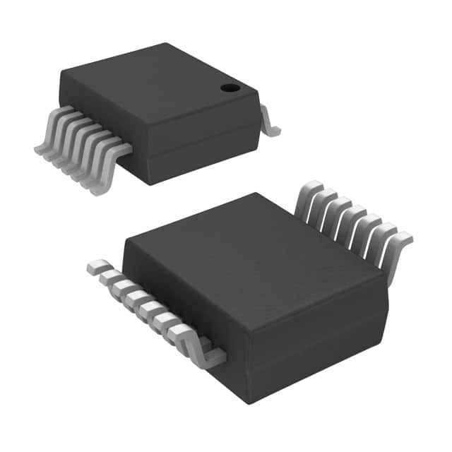
| 描述 | IC QUAD1:2 FET MUX/DEMUX 16TVSOP多路器开关 IC 4-Bit One-of-2 FET Mltplxr/Demltplxr |
| 产品分类 | |
| 品牌 | Texas Instruments |
| 产品手册 | |
| 产品图片 |
|
| rohs | 符合RoHS无铅 / 符合限制有害物质指令(RoHS)规范要求 |
| 产品系列 | 开关 IC,多路器开关 IC,Texas Instruments SN74CB3Q3257DGVR74CB |
| 数据手册 | |
| 产品型号 | SN74CB3Q3257DGVR |
| 产品目录页面 | |
| 产品种类 | 多路器开关 IC |
| 传播延迟时间 | 0.2 ns |
| 供应商器件封装 | 16-TVSOP |
| 其它名称 | 296-19137-1 |
| 包装 | 剪切带 (CT) |
| 单位重量 | 42 mg |
| 商标 | Texas Instruments |
| 安装类型 | 表面贴装 |
| 安装风格 | SMD/SMT |
| 导通电阻—最大值 | 9 Ohms |
| 封装 | Reel |
| 封装/外壳 | 16-TFSOP (0.173",4.40mm 宽) |
| 封装/箱体 | TVSOP-16 |
| 工作温度 | -40°C ~ 85°C |
| 工作电源电压 | 2.3 V to 3.6 V |
| 工作电源电流 | 1.5 mA |
| 工厂包装数量 | 2000 |
| 带宽 | 500 MHz |
| 开关数量 | 1 |
| 开关配置 | 4 x SPDT (4 x 1:2) |
| 最大工作温度 | + 85 C |
| 最小工作温度 | - 40 C |
| 标准包装 | 1 |
| 独立电路 | 1 |
| 电压-电源 | 2.3 V ~ 3.6 V |
| 电压源 | 单电源 |
| 电流-输出高,低 | - |
| 电路 | 4 x 2:1 |
| 类型 | FET 多路复用器/多路分解器 |
| 系列 | SN74CB3Q3257 |
| 通道数量 | 1 Channel |


PDF Datasheet 数据手册内容提取
Product Order Technical Tools & Support & Folder Now Documents Software Community SN74CB3Q3257 SCDS135D–SEPTEMBER2003–REVISEDJULY2018 SN74CB3Q3257 4-Bit 1-of-2 FET Multiplexer/Demultiplexer 2.5-V/3.3-V Low-Voltage High-Bandwidth Bus Switch 1 Features 2 Applications • High-BandwidthDataPath • IPPhones:WiredandWireless 1 (upto500MHz) • OpticalModules • 5-VTolerantI/OsWithDevicePoweredUpor • OpticalNetworking:VideoOverFiberandEPON PoweredDown • PrivateBranchExchange(PBX) • LowandFlatON-StateResistance(r ) on • WiMAXandWirelessInfrastructureEquipment CharacteristicsOverOperatingRange (ron=4ΩTypical) 3 Description • Rail-to-RailSwitchingonDataI/OPorts The SN74CB3Q3257 device is a high-bandwidth FET – 0-to5-VSwitchingWith3.3-VV busswitchutilizingachargepumptoelevatethegate CC voltage of the pass transistor, providing a low and flat – 0-to3.3-VSwitchingWith2.5-VV CC ON-stateresistance(r ). • BidirectionalDataFlowWithNear-Zero on PropagationDelay DeviceInformation(1) • LowInputandOutputCapacitanceMinimizes PARTNUMBER PACKAGE BODYSIZE(NOM) LoadingandSignalDistortion SN74CB3Q3257DGV TVSOP(16) 3.60mm×4.40mm (C =3.5pFTypical) io(OFF) SN74CB3Q3257DBQ SSOP(16) 4.90mm×3.90mm • FastSwitchingFrequency(f =20MHz OE SN74CB3Q3257PW TSSOP(16) 5.00mm×4.40mm Maximum) SN74CB3Q3257RGY VQFN(16) 4.00mm×3.50mm • DataandControlInputsProvideUndershoot (1) For all available packages, see the orderable addendum at ClampDiodes theendofthedatasheet. • LowPowerConsumption (I =0.7mATypical) LogicDiagram(PositiveLogic) CC • V OperatingRangeFrom2.3Vto3.6V 4 2 CC 1A SW 1B1 • DataI/OsSupport0-to5-VSignalingLevels 3 SW 1B2 (0.8V,1.2V,1.5V,1.8V,2.5V,3.3V,5V) 7 5 2A SW 2B1 • ControlInputsCanBeDrivenbyTTLor 6 SW 2B2 5-V/3.3-VCMOSOutputs 9 11 • I SupportsPartial-Power-DownModeOperation 3A SW 3B1 off 10 • Latch-UpPerformanceExceeds100mAPer SW 3B2 JESD78,ClassII 12 14 4A SW 4B1 • ESDPerformanceTestedPerJESD22 13 SW 4B2 – 2000-VHumanBodyModel (A114-B,ClassII) – 1000-VCharged-DeviceModel(C101) S 1 • SupportsBothDigitalandAnalogApplications: 15 OE USBInterface,DifferentialSignalInterface, BusIsolation,Low-DistortionSignalGating (1) (1) Foradditionalinformationregardingtheperformance characteristicsoftheCB3Qfamily,refertotheTIapplication report,CBT-C,CB3T,andCB3QSignal-SwitchFamilies, SCDA008. 1 An IMPORTANT NOTICE at the end of this data sheet addresses availability, warranty, changes, use in safety-critical applications, intellectualpropertymattersandotherimportantdisclaimers.PRODUCTIONDATA.
SN74CB3Q3257 SCDS135D–SEPTEMBER2003–REVISEDJULY2018 www.ti.com Table of Contents 1 Features.................................................................. 1 8.3 FeatureDescription...................................................9 2 Applications........................................................... 1 8.4 DeviceFunctionalModes..........................................9 3 Description............................................................. 1 9 ApplicationandImplementation........................ 10 4 RevisionHistory..................................................... 2 9.1 ApplicationInformation............................................10 9.2 TypicalApplication .................................................10 5 PinConfigurationandFunctions......................... 3 10 PowerSupplyRecommendations..................... 11 6 Specifications......................................................... 4 11 Layout................................................................... 11 6.1 AbsoluteMaximumRatings......................................4 6.2 ESDRatings..............................................................4 11.1 LayoutGuidelines.................................................11 6.3 RecommendedOperatingConditions.......................4 11.2 LayoutExample....................................................11 6.4 ThermalInformation..................................................5 12 DeviceandDocumentationSupport................. 12 6.5 ElectricalCharacteristics..........................................5 12.1 DocumentationSupport........................................12 6.6 SwitchingCharacteristics,V =2.5V.....................6 12.2 ReceivingNotificationofDocumentationUpdates12 CC 6.7 SwitchingCharacteristics,V =3.3V.....................6 12.3 CommunityResources..........................................12 CC 6.8 TypicalCharacteristics..............................................6 12.4 Trademarks...........................................................12 7 ParameterMeasurementInformation..................7 12.5 ElectrostaticDischargeCaution............................12 12.6 Glossary................................................................12 8 DetailedDescription.............................................. 8 13 Mechanical,Packaging,andOrderable 8.1 Overview...................................................................8 Information........................................................... 12 8.2 FunctionalBlockDiagram.........................................9 4 Revision History ChangesfromRevisionC(April2017)toRevisionD Page • Changedthepinoutimagesappearance .............................................................................................................................. 3 • AddedThermalInformationtablevalues............................................................................................................................... 5 ChangesfromRevisionB(June2015)toRevisionC Page • AddedMAXvaluesforT =–40°Cto105°CtotheElectricalCharacteristicstable.............................................................. 5 A • AddedMAXvaluesforT =–40°Cto105°CtotheSwitchingCharacteristics,V =2.5Vtable. ...................................... 6 A CC • AddedseparateSwitchingCharacteristics,V =3.3VforV =3.3V±0.3V.AddedTYPvaluesandMAXvalues CC CC forT =–40°Cto105°C......................................................................................................................................................... 6 A ChangesfromRevisionA(November2003)toRevisionB Page • RemovedOrderingInformationtable..................................................................................................................................... 1 • AddedDeviceInformationtable,PinConfigurationandFunctionssection,ESDRatingstable,FeatureDescription section,DeviceFunctionalModes,ApplicationandImplementationsection,PowerSupplyRecommendations section,Layoutsection,DeviceandDocumentationSupportsection,andMechanical,Packaging,andOrderable Informationsection ................................................................................................................................................................ 1 2 SubmitDocumentationFeedback Copyright©2003–2018,TexasInstrumentsIncorporated ProductFolderLinks:SN74CB3Q3257
SN74CB3Q3257 www.ti.com SCDS135D–SEPTEMBER2003–REVISEDJULY2018 5 Pin Configuration and Functions D,DB,DGV,DBQ,orPWPackage 16-PinSOIC,SSOPTVSOP,orTSSOP RGYPackage TopView 16-PinVQFN TopView C S VC S 1 16 VCC 1B1 2 15 OE 1 6 1B2 3 14 4B1 1 1B1 2 15 OE 1A 4 13 4B2 1B2 3 14 4B1 2B1 5 12 4A 1A 4 Thermal 13 4B2 2B2 6 11 3B1 Pad 2B1 5 12 4A 2A 7 10 3B2 2B2 6 11 3B1 GND 8 9 3A 2A 7 10 3B2 Not to scale 8 9 Not to scale D A N 3 G PinFunctions PIN I/O DESCRIPTION NAME NO. S 1 I SelectPin 1B1 2 I/O Channel1I/O1 1B2 3 I/O Channel1I/O2 1A 4 I/O Channel1common 2B1 5 I/O Channel2I/O1 2B2 6 I/O Channel2I/O2 2A 7 I/O Channel2common GND 8 — Ground 3A 9 I/O Channel3common 3B2 10 I/O Channel3I/O2 3B1 11 I/O Channel3I/O1 4A 12 I/O Channel4common 4B2 13 I/O Channel4I/O2 4B1 14 I/O Channel4I/O1 OE 15 I OutputEnable(ActiveLow) V 16 — Power CC Copyright©2003–2018,TexasInstrumentsIncorporated SubmitDocumentationFeedback 3 ProductFolderLinks:SN74CB3Q3257
SN74CB3Q3257 SCDS135D–SEPTEMBER2003–REVISEDJULY2018 www.ti.com 6 Specifications 6.1 Absolute Maximum Ratings overoperatingfree-airtemperaturerange(unlessotherwisenoted)(1) MIN MAX UNIT V Supplyvoltage –0.5 4.6 V CC V Controlinputvoltage(2)(3) –0.5 7 V IN V SwitchI/Ovoltage(2)(3)(4) –0.5 7 V I/O I Controlinputclampcurrent V <0 –50 mA IK IN I I/Oportclampcurrent V <0 –50 mA I/OK I/O I ON-stateswitchcurrent ±64 mA IO ContinuouscurrentthroughV orGND ±100 mA CC T Storagetemperature –65 150 °C stg (1) StressesbeyondthoselistedunderAbsoluteMaximumRatingsmaycausepermanentdamagetothedevice.Thesearestressratings only,andfunctionaloperationofthedeviceattheseoranyotherconditionsbeyondthoseindicatedunderRecommendedOperating Conditionsisnotimplied.Exposuretoabsolute-maximum-ratedconditionsforextendedperiodsmayaffectdevicereliability. (2) Allvoltagesarewithrespecttoground,unlessotherwisespecified. (3) Theinputandoutputvoltageratingsmaybeexceedediftheinputandoutputclamp-currentratingsareobserved. (4) V andV areusedtodenotespecificconditionsforV . I O I/O 6.2 ESD Ratings VALUE UNIT Humanbodymodel(HBM),perANSI/ESDA/JEDECJS-001(1) ±2000 V(ESD) Electrostaticdischarge Charged-devicemodel(CDM),perJEDECspecificationJESD22- V C101(2) ±1000 (1) JEDECdocumentJEP155statesthat500-VHBMallowssafemanufacturingwithastandardESDcontrolprocess. (2) JEDECdocumentJEP157statesthat250-VCDMallowssafemanufacturingwithastandardESDcontrolprocess. 6.3 Recommended Operating Conditions overoperatingfree-airtemperaturerange(unlessotherwisenoted)(1) MIN MAX UNIT V Supplyvoltage 2.3 3.6 V CC V =2.3Vto2.7V 1.7 5.5 CC V High-levelcontrolinputvoltage V IH V =2.7Vto3.6V 2 5.5 CC V =2.3Vto2.7V 0 0.7 CC V Low-levelcontrolinputvoltage V IL V =2.7Vto3.6V 0 0.8 CC V Datainput/outputvoltage 0 5.5 V I/O T Operatingfree-airtemperature –40 85 °C A (1) AllunusedcontrolinputsofthedevicemustbeheldatV orGNDtoensureproperdeviceoperation.RefertotheTIapplicationreport, CC ImplicationsofSloworFloatingCMOSInputs,SCBA004. 4 SubmitDocumentationFeedback Copyright©2003–2018,TexasInstrumentsIncorporated ProductFolderLinks:SN74CB3Q3257
SN74CB3Q3257 www.ti.com SCDS135D–SEPTEMBER2003–REVISEDJULY2018 6.4 Thermal Information SN74CB3Q3257 THERMALMETRIC(1) DBQ DGV(TVSOP) PW(TSSOP) RGY(VQFN) UNIT (SSOP) 16PINS 16PINS 16PINS 16PINS R Junction-to-ambientthermalresistance 114.3 126.0 112.7 49.1 θJA R Junction-to-case(top)thermalresistance 65.4 51.3 47.5 61.2 θJC(top) R Junction-to-boardthermalresistance 56.8 57.8 57.8 25.9 θJB °C/W ψ Junction-to-topcharacterizationparameter 18.3 5.9 6.0 2.3 JT ψ Junction-to-boardcharacterizationparameter 56.4 57.3 57.3 26.0 JB R Junction-to-case(bottom)thermalresistance - - - 11.4 θJC(bot) (1) Formoreinformationabouttraditionalandnewthermalmetrics,seetheSemiconductorandICPackageThermalMetricsapplication report. 6.5 Electrical Characteristics T =–40°Cto105°C.Typicalvaluesstatedareoverrecommendedoperatingfree-airtemperaturerange(unlessotherwise A noted)(1) PARAMETER TESTCONDITIONS MIN TYP(2) MAX UNIT VIK VCC=3.6V,II=–18mA –1.8 V IIN Controlinputs VCC=3.6V,VIN=0to5.5V ±1 µA IOZ(3) VVCI=C=0,3S.6wVitc,hVOOF=F0VtoIN5=.5VVC,CorGND ±1 µA Ioff VCC=0,VO=0to5.5V,VI=0 1 µA ICC VSCwCitc=h3O.6NVo,rIIO/OF=F0,,VIN=VCCorGND 0.7 1.5 mA ΔICC(4) Controlinputs VCC=3.6V,Oneinputat3V,OtherinputsatVCCorGND 30 µA ICCD(5) Percontrolinput VCCoCnt=ro3l.i6npVu,tAswaintcdhBingpoartts50o%pednu,tycycle 0.3 0.35 mA/MHz Cin Controlinputs VCC=3.3V,VIN=5.5V,3.3V,or0 2.5 3.5 pF Aport VCC=3.3V,SwitchOFF, 5.5 7 pF VIN=VCCorGND,VI/O=5.5V,3.3V,or0 Cio(OFF) Bport VCC=3.3V,SwitchOFF, 3.5 5 pF VIN=VCCorGND,VI/O=5.5V,3.3V,or0 Cio(ON) ABppoorrtt VVCINC==V3C.3CoVr,GSwNiDtc,hVOI/ON=, 5.5V,3.3V,or0 1100..55 1133 pF VCC=2.3V, VI=0,IO=30mA 4 8 ron(6) TYPatVCC=2.5V VI=1.7V,IO=–15mA 4 9 Ω VI=0,IO=30mA 4 6 VCC=3V VI=2.4V,IO=–15mA 4 8 (1) V andI refertocontrolinputs.V,V ,I,andI refertodataterminals. IN IN I O I O (2) AlltypicalvaluesareatV =3.3V(unlessotherwisenoted),T =25°C. CC A (3) ForI/Oports,theparameterI includestheinputleakagecurrent. OZ (4) ThisistheincreaseinsupplycurrentforeachinputthatisatthespecifiedTTLvoltagelevel,ratherthanV orGND. CC (5) Thisparameterspecifiesthedynamicpower-supplycurrentassociatedwiththeoperatingfrequencyofasinglecontrolinput(see Figure2). (6) MeasuredbythevoltagedropbetweentheAandBterminalsattheindicatedcurrentthroughtheswitch.ON-stateresistanceis determinedbythelowerofthevoltagesofthetwo(AorB)terminals. Copyright©2003–2018,TexasInstrumentsIncorporated SubmitDocumentationFeedback 5 ProductFolderLinks:SN74CB3Q3257
SN74CB3Q3257 SCDS135D–SEPTEMBER2003–REVISEDJULY2018 www.ti.com 6.6 Switching Characteristics, V = 2.5 V CC Typicalvaluesstatedareoverrecommendedoperatingfree-airtemperaturerange(unlessotherwisenoted)(seeFigure3) VCC=2.5V±0.2V FROM TO PARAMETER (INPUT) (OUTPUT) MIN MAX MAX UNIT (85°C) (105°C) fOEorfS(1) OEorS AorB 10 10 MHz tpd(2) AorB BorA 0.12 0.21 ns tpd(s) S A 1.5 6.5 7.5 ns S B 1.5 6.5 7.5 ten ns OE AorB 1.5 6.5 7.5 S B 1 6 7 tdis ns OE AorB 1 6 7 (1) Maximumswitchingfrequencyforcontrolinputs(V >V ,V =5V,R ≥1MΩ,C =0). O CC I L L (2) ThepropagationdelayisthecalculatedRCtimeconstantofthetypicalon-stateresistanceoftheswitchandthespecifiedload capacitance,whendrivenbyanidealvoltagesource(zerooutputimpedance). 6.7 Switching Characteristics, V = 3.3 V CC Typicalvaluesstatedareoveroperatingfree-airtemperaturerange(unlessotherwisenoted) VCC=3.3V±0.3V FROM TO PARAMETER (INPUT) (OUTPUT) MIN TYP(1) MAX MAX UNIT (85°C) (105°C) fOEorfS(2) OEorS AorB 20 20 MHz tpd(3) AorB BorA 0.2 0.32 ns tpd(s) S A 1.5 4.1 5.5 6.5 ns S B 1.5 4.6 5.5 6.5 ten ns OE AorB 1.5 4.7 5.5 6.5 S B 1 3.3 6 7 tdis ns OE AorB 1 3.1 6 7 (1) TYPtakenfromaveragein105°C (2) Maximumswitchingfrequencyforcontrolinputs(V >V ,V =5V,R ≥1MΩ,C =0). O CC I L L (3) ThepropagationdelayisthecalculatedRCtimeconstantofthetypicalon-stateresistanceoftheswitchandthespecifiedload capacitance,whendrivenbyanidealvoltagesource(zerooutputimpedance). 6.8 Typical Characteristics 12 16 VCC = 3.3 V 14 VCC = 3.3 V 10 TA = 25°C (cid:159) TA = 25°C A and B Ports Open e - 12 IO = -15 mA c 8 n sta10 mA 6 Resi 8 I - CC S Switching State 6 4 N- O 4 – 2 OE Switching R on 2 0 0 0 2 4 6 8 10 12 14 16 18 20 0 0.5 1.0 1.5 2.0 2.5 3.0 3.5 4.0 4.5 5.0 OE or S Switching Frequency - MHz V - V I Figure1.Typicalr vsV Figure2.TypicalI vsOEorSSwitchingFrequency on I CC 6 SubmitDocumentationFeedback Copyright©2003–2018,TexasInstrumentsIncorporated ProductFolderLinks:SN74CB3Q3257
SN74CB3Q3257 www.ti.com SCDS135D–SEPTEMBER2003–REVISEDJULY2018 7 Parameter Measurement Information VCC Input Generator VIN 50Ω VG1 50Ω TEST CIRCUIT DUT 2×VCC Input Generator S1 VI VO RL Open GND 50Ω VG2 50Ω CL RL (see NoteA) TEST VCC S1 RL VI CL V∆ tpd(s) 2.5 V±0.2 V Open 500Ω VCCor GND 30 pF 3.3 V±0.3 V Open 500Ω VCCor GND 50 pF tPLZ/tPZL 2.5 V±0.2 V 2×VCC 500Ω GND 30 pF 0.15 V 3.3 V±0.3 V 2×VCC 500Ω GND 50 pF 0.3 V tPHZ/tPZH 2.5 V±0.2 V GND 500Ω VCC 30 pF 0.15 V 3.3 V±0.3 V GND 500Ω VCC 50 pF 0.3 V Output VCC Control VCC/2 VCC/2 (VIN) 0 V tPZL tPLZ Output Output VCC Waveform 1 VCC Control VCC/2 VCC/2 S1 at 2×VCC VCC/2 VOL+ VD (VIN) 0 V (see Note B) VOL tPZH tPHZ tPLH tPHL Output VOH VOH Waveform 2 VOH−VD Output VCC/2 VCC/2 S1 at GND VCC/2 VOL (see Note B) 0 V VOLTAGE WAVEFORMS VOLTAGE WAVEFORMS PROPAGATION DELAYTIMES ENABLEAND DISABLE TIMES NOTES: A. CLincludes probe and jig capacitance. B. Waveform 1 is for an output with internal conditions such that the output is low, except when disabled by the output control. Waveform 2 is for an output with internal conditions such that the output is high, except when disabled by the output control. C. All input pulses are supplied by generators having the following characteristics: PRR≤10 MHz, ZO= 50W, tr≤2.5 ns, tf≤2.5 ns. D. The outputs are measured one at a time, with one transition per measurement. E. tPLZand tPHZare the same as tdis. F. tPZLand tPZHare the same as ten. G. tPLHand tPHLare the same as tpd(s).The tpdpropagation delay is the calculated RC time constant of the typical ON-state resistance ofthe switch and the specified load capacitance, when driven by an ideal voltage source (zero output impedance). H. All parameters and waveforms are not applicable to all devices. Figure3. LoadCircuitandVoltageWaveforms Copyright©2003–2018,TexasInstrumentsIncorporated SubmitDocumentationFeedback 7 ProductFolderLinks:SN74CB3Q3257
SN74CB3Q3257 SCDS135D–SEPTEMBER2003–REVISEDJULY2018 www.ti.com 8 Detailed Description 8.1 Overview The SN74CB3Q3257 device is a high-bandwidth FET bus switch using a charge pump to elevate the gate voltage of the pass transistor, providing a low and flat ON-state resistance (r ). The low and flat ON-state on resistance allows for minimal propagation delay and supports rail-to-rail switching on the data input/output (I/O) ports. The device also features low data I/O capacitance to minimize capacitive loading and signal distortion on the data bus. Specifically designed to support high-bandwidth applications, the SN74CB3Q3257 device provides an optimized interface solution ideally suited for broadband communications, networking, and data-intensive computingsystems. The SN74CB3Q3257 device is organized as two 1-of-4 multiplexers/demultiplexers with separate output-enable (1OE, 2OE) inputs. The select (S0, S1) inputs control the data path of each multiplexer/demultiplexer. When OE is low, the associated multiplexer/demultiplexer is enabled, and the A port is connected to the B port, allowing bidirectional data flow between ports. When OE is high, the associated multiplexer/demultiplexer is disabled, and ahigh-impedancestateexistsbetweentheAandBports. This device is fully specified for partial-power-down applications using I . The I circuitry prevents damaging off off currentbackflowthroughthedevicewhenitispowereddown.Thedevicehasisolationduringpoweroff. To ensure the high-impedance state during power up or power down, OE should be tied to V through a pullup CC resistor;theminimumvalueoftheresistorisdeterminedbythecurrent-sinkingcapabilityofthedriver. A B VCC Charge Pump EN(1) (1)ENistheinternalenablesignalappliedtotheswitch. Figure4. SimplifiedSchematic,EachFETSwitch(SW) 8 SubmitDocumentationFeedback Copyright©2003–2018,TexasInstrumentsIncorporated ProductFolderLinks:SN74CB3Q3257
SN74CB3Q3257 www.ti.com SCDS135D–SEPTEMBER2003–REVISEDJULY2018 8.2 Functional Block Diagram 4 2 1A SW 1B1 3 SW 1B2 7 5 2A SW 2B1 6 SW 2B2 9 11 3A SW 3B1 10 SW 3B2 12 14 4A SW 4B1 13 SW 4B2 1 S 15 OE 8.3 Feature Description The SN74CB3Q3257 device has a high-bandwidth data path (up to 500 MHz) and has 5-V tolerant I/Os with the device powered up or powered down. It also has low and flat ON-state resistance (r ) characteristics over on operatingrange(r =4 ΩTypical). on This device also has rail-to-rail switching on data I/O ports for 0- to 5-V switching with 3.3-V V and 0- to 3.3-V CC switching with 2.5-V V as well as bidirectional data flow with near-zero propagation delay and low input/output CC capacitancethatminimizesloadingandsignaldistortion(C =3.5pFTypical). io(OFF) The SN74CB3Q3257 also provides a fast switching frequency (f = 20 MHz Max) with data and control inputs OE thatprovideundershootclampdiodesaswellaslowpowerconsumption(I =0.6mATypical). CC The V operating range is from 2.3 V to 3.6 V and the data I/Os support 0- to 5-V signal levels of (0.8-V, 1.2-V, CC 1.5-V,1.8-V,2.5-V,3.3-V,5-V). The control inputs can be driven by TTL or 5-V / 3.3-V CMOS outputs as well as I Supports Partial-Power- off DownModeOperation. 8.4 Device Functional Modes Table1liststhefunctionalmodesoftheSN74CB3Q3257. Table1.FunctionTable INPUTS INPUT/OUTPUT FUNCTION OE S A L L B1 Aport=B1port L H B2 Aport=B2port H X Z Disconnect Copyright©2003–2018,TexasInstrumentsIncorporated SubmitDocumentationFeedback 9 ProductFolderLinks:SN74CB3Q3257
SN74CB3Q3257 SCDS135D–SEPTEMBER2003–REVISEDJULY2018 www.ti.com 9 Application and Implementation NOTE Information in the following applications sections is not part of the TI component specification, and TI does not warrant its accuracy or completeness. TI’s customers are responsible for determining suitability of components for their purposes. Customers should validateandtesttheirdesignimplementationtoconfirmsystemfunctionality. 9.1 Application Information The SN74CB3Q3257 can be used to multiplex and demultiplex up to 4 channels simultaneously in a 2:1 configuration. The application shown here is a 4-bit bus being multiplexed between two devices. the OE and S pinsareusedtocontrolthechipfromthebuscontroller.Thisisaverygenericexample,andcouldapplytomany situations. If an application requires less than 4 bits, be sure to tie the A side to either high or low on unused channels. 9.2 Typical Application VCC SN74CB3Q3257 VCC S 16 1 1B1 0.1 PF 1A RON 2 4 1B2 3 2B1 4 2A RON 5 Device 1 7 2B2 Bus 4 6 Controller 3B1 3A RON 11 9 3B2 10 4 Device 2 4B1 4A RON 14 12 4B2 13 GND OE 8 15 Figure5. TypicalApplicationoftheSN74CB3Q3257 9.2.1 DesignRequirements 1. RecommendedInputConditions: – Forspecifiedhighandlowlevels,seeV andV inRecommendedOperatingConditions. IH IL – Inputsandoutputsareovervoltagetolerantslowingthemtogoashighas4.6VatanyvalidV . CC 2. RecommendedOutputConditions: – Loadcurrentsshouldnotexceed ±128mAperchannel. 3. FrequencySelectionCriterion: – Maximumfrequencytestedis500MHz. – Added trace resistance/capacitance can reduce maximum frequency capability; use layout practices as directedinLayout. 9.2.2 DetailedDesignProcedure The0.1-µFcapacitorshouldbeplaceascloseaspossibletothedevice. 10 SubmitDocumentationFeedback Copyright©2003–2018,TexasInstrumentsIncorporated ProductFolderLinks:SN74CB3Q3257
SN74CB3Q3257 www.ti.com SCDS135D–SEPTEMBER2003–REVISEDJULY2018 Typical Application (continued) 9.2.3 ApplicationCurve 3 2 V) e ( g a olt V 1 VIN VOUT 0 0 100 200 300 400 500 600 700 800 900 1000 Time (ps) C001 Figure6. PropagationDelay(t )SimulationResultatV =2.5V. pd CC 10 Power Supply Recommendations The power supply can be any voltage between the minimum and maximum supply voltage rating listed in the AbsoluteMaximumRatingstable. Each V terminal should have a good bypass capacitor to prevent power disturbance. For devices with a single CC supply, a 0.1-μF bypass capacitor is recommended. If multiple pins are labeled V , then a 0.01-μF or 0.022-μF CC capacitor is recommended for each V because the V pins are tied together internally. For devices with dual- CC CC supply pins operating at different voltages, for example V and V , a 0.1-µF bypass capacitor is recommended CC DD foreachsupplypin.Torejectdifferentfrequenciesofnoise,usemultiplebypasscapacitorsinparallel.Capacitors with values of 0.1 μF and 1 μF are commonly used in parallel. The bypass capacitor should be installed as close tothepowerterminalaspossibleforbestresults. 11 Layout 11.1 Layout Guidelines Reflections and matching are closely related to the loop antenna theory but are different enough to be discussed separately from the theory. When a PCB trace turns a corner at a 90° angle, a reflection can occur. A reflection occurs primarily because of the change of width of the trace. At the apex of the turn, the trace width increases to 1.414 times the width. This increase upsets the transmission-line characteristics, especially the distributed capacitance and self–inductance of the trace which results in the reflection. Not all PCB traces can be straight and therefore some traces must turn corners. Figure 7 shows progressively better techniques of rounding corners.Onlythelastexample(BEST)maintainsconstanttracewidthandminimizesreflections. 11.2 Layout Example WORST BETTER BEST W 2 1W min. W Figure7. TraceExample Copyright©2003–2018,TexasInstrumentsIncorporated SubmitDocumentationFeedback 11 ProductFolderLinks:SN74CB3Q3257
SN74CB3Q3257 SCDS135D–SEPTEMBER2003–REVISEDJULY2018 www.ti.com 12 Device and Documentation Support 12.1 Documentation Support 12.1.1 RelatedDocumentation Forrelateddocumentationseethefollowing: • ImplicationsofSloworFloatingCMOSInputs,SCBA004 • SelectingtheRightTexasInstrumentsSignalSwitch,SZZA030 12.2 Receiving Notification of Documentation Updates To receive notification of documentation updates, navigate to the device product folder on ti.com. In the upper right corner, click on Alert me to register and receive a weekly digest of any product information that has changed.Forchangedetails,reviewtherevisionhistoryincludedinanyreviseddocument. 12.3 Community Resources The following links connect to TI community resources. Linked contents are provided "AS IS" by the respective contributors. They do not constitute TI specifications and do not necessarily reflect TI's views; see TI's Terms of Use. TIE2E™OnlineCommunity TI'sEngineer-to-Engineer(E2E)Community.Createdtofostercollaboration amongengineers.Ate2e.ti.com,youcanaskquestions,shareknowledge,exploreideasandhelp solveproblemswithfellowengineers. DesignSupport TI'sDesignSupport QuicklyfindhelpfulE2Eforumsalongwithdesignsupporttoolsand contactinformationfortechnicalsupport. 12.4 Trademarks E2EisatrademarkofTexasInstruments. Allothertrademarksarethepropertyoftheirrespectiveowners. 12.5 Electrostatic Discharge Caution Thesedeviceshavelimitedbuilt-inESDprotection.Theleadsshouldbeshortedtogetherorthedeviceplacedinconductivefoam duringstorageorhandlingtopreventelectrostaticdamagetotheMOSgates. 12.6 Glossary SLYZ022—TIGlossary. Thisglossarylistsandexplainsterms,acronyms,anddefinitions. 13 Mechanical, Packaging, and Orderable Information The following pages include mechanical, packaging, and orderable information. This information is the most current data available for the designated devices. This data is subject to change without notice and revision of thisdocument.Forbrowser-basedversionsofthisdatasheet,refertotheleft-handnavigation. 12 SubmitDocumentationFeedback Copyright©2003–2018,TexasInstrumentsIncorporated ProductFolderLinks:SN74CB3Q3257
PACKAGE OPTION ADDENDUM www.ti.com 6-Feb-2020 PACKAGING INFORMATION Orderable Device Status Package Type Package Pins Package Eco Plan Lead/Ball Finish MSL Peak Temp Op Temp (°C) Device Marking Samples (1) Drawing Qty (2) (6) (3) (4/5) 74CB3Q3257DBQRE4 ACTIVE SSOP DBQ 16 2500 Green (RoHS NIPDAU Level-2-260C-1 YEAR -40 to 85 BU257 & no Sb/Br) 74CB3Q3257RGYRG4 ACTIVE VQFN RGY 16 3000 Green (RoHS NIPDAU Level-2-260C-1 YEAR -40 to 85 BU257 & no Sb/Br) SN74CB3Q3257DBQR ACTIVE SSOP DBQ 16 2500 Green (RoHS NIPDAU Level-2-260C-1 YEAR -40 to 85 BU257 & no Sb/Br) SN74CB3Q3257DGVR ACTIVE TVSOP DGV 16 2000 Green (RoHS NIPDAU Level-1-260C-UNLIM -40 to 85 BU257 & no Sb/Br) SN74CB3Q3257PW ACTIVE TSSOP PW 16 90 Green (RoHS NIPDAU Level-1-260C-UNLIM -40 to 85 BU257 & no Sb/Br) SN74CB3Q3257PWE4 ACTIVE TSSOP PW 16 90 Green (RoHS NIPDAU Level-1-260C-UNLIM -40 to 85 BU257 & no Sb/Br) SN74CB3Q3257PWG4 ACTIVE TSSOP PW 16 90 Green (RoHS NIPDAU Level-1-260C-UNLIM -40 to 85 BU257 & no Sb/Br) SN74CB3Q3257PWR ACTIVE TSSOP PW 16 2000 Green (RoHS NIPDAU | SN Level-1-260C-UNLIM -40 to 85 BU257 & no Sb/Br) SN74CB3Q3257PWRG4 ACTIVE TSSOP PW 16 2000 Green (RoHS NIPDAU Level-1-260C-UNLIM -40 to 85 BU257 & no Sb/Br) SN74CB3Q3257RGYR ACTIVE VQFN RGY 16 3000 Green (RoHS NIPDAU Level-2-260C-1 YEAR -40 to 85 BU257 & no Sb/Br) (1) The marketing status values are defined as follows: ACTIVE: Product device recommended for new designs. LIFEBUY: TI has announced that the device will be discontinued, and a lifetime-buy period is in effect. NRND: Not recommended for new designs. Device is in production to support existing customers, but TI does not recommend using this part in a new design. PREVIEW: Device has been announced but is not in production. Samples may or may not be available. OBSOLETE: TI has discontinued the production of the device. (2) RoHS: TI defines "RoHS" to mean semiconductor products that are compliant with the current EU RoHS requirements for all 10 RoHS substances, including the requirement that RoHS substance do not exceed 0.1% by weight in homogeneous materials. Where designed to be soldered at high temperatures, "RoHS" products are suitable for use in specified lead-free processes. TI may reference these types of products as "Pb-Free". RoHS Exempt: TI defines "RoHS Exempt" to mean products that contain lead but are compliant with EU RoHS pursuant to a specific EU RoHS exemption. Green: TI defines "Green" to mean the content of Chlorine (Cl) and Bromine (Br) based flame retardants meet JS709B low halogen requirements of <=1000ppm threshold. Antimony trioxide based flame retardants must also meet the <=1000ppm threshold requirement. (3) MSL, Peak Temp. - The Moisture Sensitivity Level rating according to the JEDEC industry standard classifications, and peak solder temperature. Addendum-Page 1
PACKAGE OPTION ADDENDUM www.ti.com 6-Feb-2020 (4) There may be additional marking, which relates to the logo, the lot trace code information, or the environmental category on the device. (5) Multiple Device Markings will be inside parentheses. Only one Device Marking contained in parentheses and separated by a "~" will appear on a device. If a line is indented then it is a continuation of the previous line and the two combined represent the entire Device Marking for that device. (6) Lead/Ball Finish - Orderable Devices may have multiple material finish options. Finish options are separated by a vertical ruled line. Lead/Ball Finish values may wrap to two lines if the finish value exceeds the maximum column width. Important Information and Disclaimer:The information provided on this page represents TI's knowledge and belief as of the date that it is provided. TI bases its knowledge and belief on information provided by third parties, and makes no representation or warranty as to the accuracy of such information. Efforts are underway to better integrate information from third parties. TI has taken and continues to take reasonable steps to provide representative and accurate information but may not have conducted destructive testing or chemical analysis on incoming materials and chemicals. TI and TI suppliers consider certain information to be proprietary, and thus CAS numbers and other limited information may not be available for release. In no event shall TI's liability arising out of such information exceed the total purchase price of the TI part(s) at issue in this document sold by TI to Customer on an annual basis. Addendum-Page 2
PACKAGE MATERIALS INFORMATION www.ti.com 17-Apr-2020 TAPE AND REEL INFORMATION *Alldimensionsarenominal Device Package Package Pins SPQ Reel Reel A0 B0 K0 P1 W Pin1 Type Drawing Diameter Width (mm) (mm) (mm) (mm) (mm) Quadrant (mm) W1(mm) SN74CB3Q3257DBQR SSOP DBQ 16 2500 330.0 12.5 6.4 5.2 2.1 8.0 12.0 Q1 SN74CB3Q3257DGVR TVSOP DGV 16 2000 330.0 12.4 6.8 4.0 1.6 8.0 12.0 Q1 SN74CB3Q3257PWR TSSOP PW 16 2000 330.0 12.4 6.9 5.6 1.6 8.0 12.0 Q1 SN74CB3Q3257PWR TSSOP PW 16 2000 330.0 12.4 6.9 5.6 1.6 8.0 12.0 Q1 SN74CB3Q3257PWRG4 TSSOP PW 16 2000 330.0 12.4 6.9 5.6 1.6 8.0 12.0 Q1 SN74CB3Q3257RGYR VQFN RGY 16 3000 330.0 12.4 3.8 4.3 1.5 8.0 12.0 Q1 PackMaterials-Page1
PACKAGE MATERIALS INFORMATION www.ti.com 17-Apr-2020 *Alldimensionsarenominal Device PackageType PackageDrawing Pins SPQ Length(mm) Width(mm) Height(mm) SN74CB3Q3257DBQR SSOP DBQ 16 2500 340.5 338.1 20.6 SN74CB3Q3257DGVR TVSOP DGV 16 2000 367.0 367.0 35.0 SN74CB3Q3257PWR TSSOP PW 16 2000 367.0 367.0 35.0 SN74CB3Q3257PWR TSSOP PW 16 2000 364.0 364.0 27.0 SN74CB3Q3257PWRG4 TSSOP PW 16 2000 367.0 367.0 35.0 SN74CB3Q3257RGYR VQFN RGY 16 3000 367.0 367.0 35.0 PackMaterials-Page2
PACKAGE OUTLINE PW0016A TSSOP - 1.2 mm max height SCALE 2.500 SMALL OUTLINE PACKAGE SEATING PLANE C 6.6 TYP 6.2 A 0.1 C PIN 1 INDEX AREA 14X 0.65 16 1 2X 5.1 4.55 4.9 NOTE 3 8 9 0.30 B 4.5 16X 0.19 1.2 MAX 4.3 0.1 C A B NOTE 4 (0.15) TYP SEE DETAIL A 0.25 GAGE PLANE 0.15 0.05 0.75 0.50 0 -8 DETA 20AIL A TYPICAL 4220204/A 02/2017 NOTES: 1. All linear dimensions are in millimeters. Any dimensions in parenthesis are for reference only. Dimensioning and tolerancing per ASME Y14.5M. 2. This drawing is subject to change without notice. 3. This dimension does not include mold flash, protrusions, or gate burrs. Mold flash, protrusions, or gate burrs shall not exceed 0.15 mm per side. 4. This dimension does not include interlead flash. Interlead flash shall not exceed 0.25 mm per side. 5. Reference JEDEC registration MO-153. www.ti.com
EXAMPLE BOARD LAYOUT PW0016A TSSOP - 1.2 mm max height SMALL OUTLINE PACKAGE 16X (1.5) SYMM (R0.05) TYP 1 16X (0.45) 16 SYMM 14X (0.65) 8 9 (5.8) LAND PATTERN EXAMPLE EXPOSED METAL SHOWN SCALE: 10X SOLDER MASK METAL UNDER SOLDER MASK OPENING METAL SOLDER MASK OPENING EXPOSED METAL EXPOSED METAL 0.05 MAX 0.05 MIN ALL AROUND ALL AROUND NON-SOLDER MASK SOLDER MASK DEFINED DEFINED (PREFERRED) SOLDE15.000R MASK DETAILS 4220204/A 02/2017 NOTES: (continued) 6. Publication IPC-7351 may have alternate designs. 7. Solder mask tolerances between and around signal pads can vary based on board fabrication site. www.ti.com
EXAMPLE STENCIL DESIGN PW0016A TSSOP - 1.2 mm max height SMALL OUTLINE PACKAGE 16X (1.5) SYMM (R0.05) TYP 1 16X (0.45) 16 SYMM 14X (0.65) 8 9 (5.8) SOLDER PASTE EXAMPLE BASED ON 0.125 mm THICK STENCIL SCALE: 10X 4220204/A 02/2017 NOTES: (continued) 8. Laser cutting apertures with trapezoidal walls and rounded corners may offer better paste release. IPC-7525 may have alternate design recommendations. 9. Board assembly site may have different recommendations for stencil design. www.ti.com
MECHANICAL DATA MPDS006C – FEBRUARY 1996 – REVISED AUGUST 2000 DGV (R-PDSO-G**) PLASTIC SMALL-OUTLINE 24 PINS SHOWN 0,23 0,40 0,07 M 0,13 24 13 0,16 NOM 4,50 6,60 4,30 6,20 Gage Plane 0,25 0°–(cid:1)8° 0,75 1 12 0,50 A Seating Plane 0,15 1,20 MAX 0,08 0,05 PINS ** 14 16 20 24 38 48 56 DIM A MAX 3,70 3,70 5,10 5,10 7,90 9,80 11,40 A MIN 3,50 3,50 4,90 4,90 7,70 9,60 11,20 4073251/E 08/00 NOTES: A. All linear dimensions are in millimeters. B. This drawing is subject to change without notice. C. Body dimensions do not include mold flash or protrusion, not to exceed 0,15 per side. D. Falls within JEDEC: 24/48 Pins – MO-153 14/16/20/56 Pins – MO-194 • POST OFFICE BOX 655303 DALLAS, TEXAS 75265
None
PACKAGE OUTLINE DBQ0016A SSOP - 1.75 mm max height SCALE 2.800 SHRINK SMALL-OUTLINE PACKAGE C SEATING PLANE .228-.244 TYP [5.80-6.19] .004 [0.1] C A PIN 1 ID AREA 14X .0250 [0.635] 16 1 2X .189-.197 .175 [4.81-5.00] [4.45] NOTE 3 8 9 16X .008-.012 B .150-.157 [0.21-0.30] .069 MAX [3.81-3.98] [1.75] NOTE 4 .007 [0.17] C A B .005-.010 TYP [0.13-0.25] SEE DETAIL A .010 [0.25] GAGE PLANE .004-.010 0 - 8 [0.11-0.25] .016-.035 [0.41-0.88] DETAIL A (.041 ) TYPICAL [1.04] 4214846/A 03/2014 NOTES: 1. Linear dimensions are in inches [millimeters]. Dimensions in parenthesis are for reference only. Controlling dimensions are in inches. Dimensioning and tolerancing per ASME Y14.5M. 2. This drawing is subject to change without notice. 3. This dimension does not include mold flash, protrusions, or gate burrs. Mold flash, protrusions, or gate burrs shall not exceed .006 inch, per side. 4. This dimension does not include interlead flash. 5. Reference JEDEC registration MO-137, variation AB. www.ti.com
EXAMPLE BOARD LAYOUT DBQ0016A SSOP - 1.75 mm max height SHRINK SMALL-OUTLINE PACKAGE 16X (.063) [1.6] SYMM SEE DETAILS 1 16 16X (.016 ) [0.41] 14X (.0250 ) [0.635] 8 9 (.213) [5.4] LAND PATTERN EXAMPLE SCALE:8X SOLDER MASK SOLDER MASK METAL OPENING OPENING METAL .002 MAX .002 MIN [0.05] [0.05] ALL AROUND ALL AROUND NON SOLDER MASK SOLDER MASK DEFINED DEFINED SOLDER MASK DETAILS 4214846/A 03/2014 NOTES: (continued) 6. Publication IPC-7351 may have alternate designs. 7. Solder mask tolerances between and around signal pads can vary based on board fabrication site. www.ti.com
EXAMPLE STENCIL DESIGN DBQ0016A SSOP - 1.75 mm max height SHRINK SMALL-OUTLINE PACKAGE 16X (.063) [1.6] SYMM 1 16 16X (.016 ) [0.41] SYMM 14X (.0250 ) [0.635] 8 9 (.213) [5.4] SOLDER PASTE EXAMPLE BASED ON .005 INCH [0.127 MM] THICK STENCIL SCALE:8X 4214846/A 03/2014 NOTES: (continued) 8. Laser cutting apertures with trapezoidal walls and rounded corners may offer better paste release. IPC-7525 may have alternate design recommendations. 9. Board assembly site may have different recommendations for stencil design. www.ti.com
None
None
None
IMPORTANTNOTICEANDDISCLAIMER TI PROVIDES TECHNICAL AND RELIABILITY DATA (INCLUDING DATASHEETS), DESIGN RESOURCES (INCLUDING REFERENCE DESIGNS), APPLICATION OR OTHER DESIGN ADVICE, WEB TOOLS, SAFETY INFORMATION, AND OTHER RESOURCES “AS IS” AND WITH ALL FAULTS, AND DISCLAIMS ALL WARRANTIES, EXPRESS AND IMPLIED, INCLUDING WITHOUT LIMITATION ANY IMPLIED WARRANTIES OF MERCHANTABILITY, FITNESS FOR A PARTICULAR PURPOSE OR NON-INFRINGEMENT OF THIRD PARTY INTELLECTUAL PROPERTY RIGHTS. These resources are intended for skilled developers designing with TI products. You are solely responsible for (1) selecting the appropriate TI products for your application, (2) designing, validating and testing your application, and (3) ensuring your application meets applicable standards, and any other safety, security, or other requirements. These resources are subject to change without notice. TI grants you permission to use these resources only for development of an application that uses the TI products described in the resource. Other reproduction and display of these resources is prohibited. No license is granted to any other TI intellectual property right or to any third party intellectual property right. TI disclaims responsibility for, and you will fully indemnify TI and its representatives against, any claims, damages, costs, losses, and liabilities arising out of your use of these resources. TI’s products are provided subject to TI’s Terms of Sale (www.ti.com/legal/termsofsale.html) or other applicable terms available either on ti.com or provided in conjunction with such TI products. TI’s provision of these resources does not expand or otherwise alter TI’s applicable warranties or warranty disclaimers for TI products. Mailing Address: Texas Instruments, Post Office Box 655303, Dallas, Texas 75265 Copyright © 2020, Texas Instruments Incorporated