ICGOO在线商城 > 集成电路(IC) > 逻辑 - 信号开关,多路复用器,解码器 > SN74HC148N
 Datasheet下载
- 型号: SN74HC148N
- 制造商: Texas Instruments
- 库位|库存: xxxx|xxxx
- 要求:
| 数量阶梯 | 香港交货 | 国内含税 |
| +xxxx | $xxxx | ¥xxxx |
查看当月历史价格
查看今年历史价格
SN74HC148N产品简介:
ICGOO电子元器件商城为您提供SN74HC148N由Texas Instruments设计生产,在icgoo商城现货销售,并且可以通过原厂、代理商等渠道进行代购。 SN74HC148N价格参考¥1.04-¥1.04。Texas InstrumentsSN74HC148N封装/规格:逻辑 - 信号开关,多路复用器,解码器, Priority Encoder 1 x 8:3 16-PDIP。您可以下载SN74HC148N参考资料、Datasheet数据手册功能说明书,资料中有SN74HC148N 详细功能的应用电路图电压和使用方法及教程。
SN74HC148N 是德州仪器(Texas Instruments)生产的一款 8 线到 3 线优先级编码器,属于逻辑电路中的编码器类别。它广泛应用于需要将多个输入信号转换为二进制编码输出的数字系统中。

典型应用场景包括:

1. 键盘扫描:在计算机或控制面板中,用于将多个按键输入压缩为少量的编码线,提升接口效率。
2. 中断请求管理:在微处理器系统中,用于识别多个中断源中优先级最高的请求。
3. 数据选择与控制:在工业控制系统中,用于从多个传感器或执行器中选择一个进行处理。
4. 通信设备:用于信号路由和通道选择,简化硬件设计。
5. 测试与测量仪器:用于多路信号采集系统的前端选择控制。

该器件具有优先级功能,确保在多个输入同时有效时,仅对优先级最高的输入进行编码,适用于需快速响应关键信号的场合。其工作电压范围宽、功耗低、抗干扰能力强,适合工业环境应用。
| 参数 | 数值 |
| 产品目录 | 集成电路 (IC)半导体 |
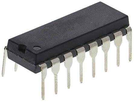
| 描述 | IC 8-TO-3 PRIORITY ENCOD 16-DIP编码器、解码器、复用器和解复用器 8-to-3 Line Priority |
| 产品分类 | |
| 品牌 | Texas Instruments |
| 产品手册 | |
| 产品图片 |
|
| rohs | 符合RoHS无铅 / 符合限制有害物质指令(RoHS)规范要求 |
| 产品系列 | 逻辑集成电路,编码器、解码器、复用器和解复用器,Texas Instruments SN74HC148N74HC |
| 数据手册 | |
| 产品型号 | SN74HC148N |
| PCN设计/规格 | |
| 产品 | Priority Encoders |
| 产品目录页面 | |
| 产品种类 | 编码器、解码器、复用器和解复用器 |
| 传播延迟时间 | 16 ns |
| 供应商器件封装 | 16-PDIP |
| 其它名称 | 296-8233-5 |
| 包装 | 管件 |
| 单位重量 | 1 g |
| 商标 | Texas Instruments |
| 安装类型 | 通孔 |
| 安装风格 | Through Hole |
| 封装 | Tube |
| 封装/外壳 | 16-DIP(0.300",7.62mm) |
| 封装/箱体 | PDIP-16 |
| 工作温度 | -40°C ~ 85°C |
| 工作温度范围 | - 40 C to + 85 C |
| 工作电压 | 2 V to 6 V |
| 工厂包装数量 | 25 |
| 最大工作温度 | + 85 C |
| 最小工作温度 | - 40 C |
| 标准包装 | 25 |
| 独立电路 | 1 |
| 电压-电源 | 2 V ~ 6 V |
| 电压源 | 单电源 |
| 电流-输出高,低 | 5.2mA,5.2mA |
| 电源电压-最大 | 6 V |
| 电源电压-最小 | 2 V |
| 电路 | 1 x 8:3 |
| 类型 | 优先顺序编码器 |
| 系列 | SN74HC148 |
| 输入/输出线数量 | 8 / 3 |
| 输入线路数量 | 8 |
| 输出线路数量 | 3 |
| 逻辑系列 | HC |


- 商务部:美国ITC正式对集成电路等产品启动337调查
- 曝三星4nm工艺存在良率问题 高通将骁龙8 Gen1或转产台积电
- 太阳诱电将投资9.5亿元在常州建新厂生产MLCC 预计2023年完工
- 英特尔发布欧洲新工厂建设计划 深化IDM 2.0 战略
- 台积电先进制程称霸业界 有大客户加持明年业绩稳了
- 达到5530亿美元!SIA预计今年全球半导体销售额将创下新高
- 英特尔拟将自动驾驶子公司Mobileye上市 估值或超500亿美元
- 三星加码芯片和SET,合并消费电子和移动部门,撤换高东真等 CEO
- 三星电子宣布重大人事变动 还合并消费电子和移动部门
- 海关总署:前11个月进口集成电路产品价值2.52万亿元 增长14.8%


PDF Datasheet 数据手册内容提取
(cid:1)(cid:2)(cid:3)(cid:4)(cid:5)(cid:6)(cid:7)(cid:4)(cid:8)(cid:9) (cid:1)(cid:2)(cid:10)(cid:4)(cid:5)(cid:6)(cid:7)(cid:4)(cid:8) (cid:8)(cid:11)(cid:12)(cid:13)(cid:2)(cid:14) (cid:15)(cid:16) (cid:17)(cid:11)(cid:12)(cid:13)(cid:2)(cid:14) (cid:18)(cid:19)(cid:13)(cid:16)(cid:19)(cid:13)(cid:15)(cid:20) (cid:14)(cid:2)(cid:6)(cid:16)(cid:21)(cid:14)(cid:19)(cid:1) SCLS109G − MARCH 1984 − REVISED APRIL 2004 (cid:1) Wide Operating Voltage Range of 2 V to 6 V SN54HC148...J OR W PACKAGE (cid:1) SN74HC148...D, DW, N, OR NS PACKAGE Outputs Can Drive Up To 10 LSTTL Loads (TOP VIEW) (cid:1) Low Power Consumption, 80-µA Max I CC (cid:1) Typical tpd = 16 ns 4 1 16 VCC (cid:1) ±4-mA Output Drive at 5 V 5 2 15 EO (cid:1) Low Input Current of 1 µA Max 6 3 14 GS 7 4 13 3 (cid:1) Encode Eight Data Lines to 3-Line Binary EI 5 12 2 (Octal) A2 6 11 1 (cid:1) Applications Include: A1 7 10 0 − n-Bit Encoding GND 8 9 A0 − Code Converters and Generators SN54HC148...FK PACKAGE description/ordering information (TOP VIEW) The ’HC148 devices feature priority decoding of C CCO the inputs to ensure that only the highest-order 5 4 N V E data line is encoded. These devices encode eight 3 2 1 20 19 data lines to 3-line (4-2-1) binary (octal). 6 4 18 GS Cascading circuitry (enable input EI and enable 7 5 17 3 output EO) has been provided to allow octal NC 6 16 NC expansion without the need for external circuitry. EI 7 15 2 Data inputs and outputs are active at the low logic A2 8 14 1 9 10 1112 13 level. 1D C 00 AN N A G NC − No internal connection ORDERING INFORMATION ORDERABLE TOP-SIDE TA PACKAGE† PART NUMBER MARKING PDIP − N Tube of 25 SN74HC148N SN74HC148N Tube of 40 SN74HC148D SSOOIICC −− DD Reel of 2500 SN74HC148DR HHCC114488 −−4400°°CC ttoo 8855°°CC Reel of 250 SN74HC148DT SOIC − DW Reel of 2000 SN74HC148DWR HC148 SOP − NS Reel of 2000 SN74HC148NSR HC148 CDIP − J Tube of 25 SNJ54HC148J SNJ54HC148J −−5555°CC ttoo 112255°CC CFP − W Tube of 150 SNJ54HC148W SNJ54HC148W LCCC − FK Tube of 55 SNJ54HC148FK SNJ54HC148FK †Package drawings, standard packing quantities, thermal data, symbolization, and PCB design guidelines are available at www.ti.com/sc/package. Please be aware that an important notice concerning availability, standard warranty, and use in critical applications of TexasInstruments semiconductor products and disclaimers thereto appears at the end of this data sheet. (cid:18)(cid:19)(cid:16)(cid:21)(cid:22)(cid:6)(cid:15)(cid:13)(cid:16)(cid:2) (cid:21)(cid:23)(cid:15)(cid:23) (cid:24)(cid:25)(cid:26)(cid:27)(cid:28)(cid:29)(cid:30)(cid:31)(cid:24)(cid:27)(cid:25) (cid:24)! "#(cid:28)(cid:28)$(cid:25)(cid:31) (cid:30)! (cid:27)(cid:26) %#&’(cid:24)"(cid:30)(cid:31)(cid:24)(cid:27)(cid:25) ((cid:30)(cid:31)$) Copyright 2004, Texas Instruments Incorporated (cid:18)(cid:28)(cid:27)(#"(cid:31)! "(cid:27)(cid:25)(cid:26)(cid:27)(cid:28)(cid:29) (cid:31)(cid:27) !%$"(cid:24)(cid:26)(cid:24)"(cid:30)(cid:31)(cid:24)(cid:27)(cid:25)! %$(cid:28) (cid:31)*$ (cid:31)$(cid:28)(cid:29)! (cid:27)(cid:26) (cid:15)$+(cid:30)! (cid:13)(cid:25)!(cid:31)(cid:28)#(cid:29)$(cid:25)(cid:31)! (cid:16)(cid:25) %(cid:28)(cid:27)(#"(cid:31)! "(cid:27)(cid:29)%’(cid:24)(cid:30)(cid:25)(cid:31) (cid:31)(cid:27) /(cid:13)(cid:12)(cid:11)(cid:18)(cid:19)0(cid:11)(cid:17)(cid:8)(cid:3)(cid:17)(cid:3)(cid:9) (cid:30)’’ %(cid:30)(cid:28)(cid:30)(cid:29)$(cid:31)$(cid:28)! (cid:30)(cid:28)$ (cid:31)$!(cid:31)$( !(cid:31)(cid:30)(cid:25)((cid:30)(cid:28)( ,(cid:30)(cid:28)(cid:28)(cid:30)(cid:25)(cid:31)-) (cid:18)(cid:28)(cid:27)(#"(cid:31)(cid:24)(cid:27)(cid:25) %(cid:28)(cid:27)"$!!(cid:24)(cid:25). ((cid:27)$! (cid:25)(cid:27)(cid:31) (cid:25)$"$!!(cid:30)(cid:28)(cid:24)’- (cid:24)(cid:25)"’#($ #(cid:25)’$!! (cid:27)(cid:31)*$(cid:28),(cid:24)!$ (cid:25)(cid:27)(cid:31)$() (cid:16)(cid:25) (cid:30)’’ (cid:27)(cid:31)*$(cid:28) %(cid:28)(cid:27)(#"(cid:31)!(cid:9) %(cid:28)(cid:27)(#"(cid:31)(cid:24)(cid:27)(cid:25) (cid:31)$!(cid:31)(cid:24)(cid:25). (cid:27)(cid:26) (cid:30)’’ %(cid:30)(cid:28)(cid:30)(cid:29)$(cid:31)$(cid:28)!) %(cid:28)(cid:27)"$!!(cid:24)(cid:25). ((cid:27)$! (cid:25)(cid:27)(cid:31) (cid:25)$"$!!(cid:30)(cid:28)(cid:24)’- (cid:24)(cid:25)"’#($ (cid:31)$!(cid:31)(cid:24)(cid:25). (cid:27)(cid:26) (cid:30)’’ %(cid:30)(cid:28)(cid:30)(cid:29)$(cid:31)$(cid:28)!) POST OFFICE BOX 655303 • DALLAS, TEXAS 75265 1
(cid:1)(cid:2)(cid:3)(cid:4)(cid:5)(cid:6)(cid:7)(cid:4)(cid:8)(cid:9) (cid:1)(cid:2)(cid:10)(cid:4)(cid:5)(cid:6)(cid:7)(cid:4)(cid:8) (cid:8)(cid:11)(cid:12)(cid:13)(cid:2)(cid:14) (cid:15)(cid:16) (cid:17)(cid:11)(cid:12)(cid:13)(cid:2)(cid:14) (cid:18)(cid:19)(cid:13)(cid:16)(cid:19)(cid:13)(cid:15)(cid:20) (cid:14)(cid:2)(cid:6)(cid:16)(cid:21)(cid:14)(cid:19)(cid:1) SCLS109G − MARCH 1984 − REVISED APRIL 2004 FUNCTION TABLE INPUTS OUTPUTS EI 0 1 2 3 4 5 6 7 A2 A1 A0 GS EO H X X X X X X X X H H H H H L H H H H H H H H H H H H L L X X X X X X X L L L L L H L X X X X X X L H L L H L H L X X X X X L H H L H L L H L X X X X L H H H L H H L H L X X X L H H H H H L L L H L X X L H H H H H H L H L H L X L H H H H H H H H L L H L L H H H H H H H H H H L H 2 POST OFFICE BOX 655303 • DALLAS, TEXAS 75265
(cid:1)(cid:2)(cid:3)(cid:4)(cid:5)(cid:6)(cid:7)(cid:4)(cid:8)(cid:9) (cid:1)(cid:2)(cid:10)(cid:4)(cid:5)(cid:6)(cid:7)(cid:4)(cid:8) (cid:8)(cid:11)(cid:12)(cid:13)(cid:2)(cid:14) (cid:15)(cid:16) (cid:17)(cid:11)(cid:12)(cid:13)(cid:2)(cid:14) (cid:18)(cid:19)(cid:13)(cid:16)(cid:19)(cid:13)(cid:15)(cid:20) (cid:14)(cid:2)(cid:6)(cid:16)(cid:21)(cid:14)(cid:19)(cid:1) SCLS109G − MARCH 1984 − REVISED APRIL 2004 logic diagram (positive logic) 10 0 15 EO 14 11 GS 1 12 2 9 A0 13 3 1 4 7 A1 2 5 3 6 4 7 6 A2 5 EI Pin numbers shown are for the D, DW, J, N, NS, and W packages. POST OFFICE BOX 655303 • DALLAS, TEXAS 75265 3
(cid:1)(cid:2)(cid:3)(cid:4)(cid:5)(cid:6)(cid:7)(cid:4)(cid:8)(cid:9) (cid:1)(cid:2)(cid:10)(cid:4)(cid:5)(cid:6)(cid:7)(cid:4)(cid:8) (cid:8)(cid:11)(cid:12)(cid:13)(cid:2)(cid:14) (cid:15)(cid:16) (cid:17)(cid:11)(cid:12)(cid:13)(cid:2)(cid:14) (cid:18)(cid:19)(cid:13)(cid:16)(cid:19)(cid:13)(cid:15)(cid:20) (cid:14)(cid:2)(cid:6)(cid:16)(cid:21)(cid:14)(cid:19)(cid:1) SCLS109G − MARCH 1984 − REVISED APRIL 2004 absolute maximum ratings over operating free-air temperature range (unless otherwise noted)† Supply voltage range, V . . . . . . . . . . . . . . . . . . . . . . . . . . . . . . . . . . . . . . . . . . . . . . . . . . . . . . . . . . −0.5 V to 7 V CC Input clamp current, I (V < 0 or V > V ) (see Note 1) . . . . . . . . . . . . . . . . . . . . . . . . . . . . . . . . . . . . ±20 mA IK I I CC Output clamp current, I (V < 0 or V > V ) (see Note 1) . . . . . . . . . . . . . . . . . . . . . . . . . . . . . . . . ±20 mA OK O O CC Continuous output current, I (V = 0 to V ) . . . . . . . . . . . . . . . . . . . . . . . . . . . . . . . . . . . . . . . . . . . . . . ±25 mA O O CC Continuous current through V or GND . . . . . . . . . . . . . . . . . . . . . . . . . . . . . . . . . . . . . . . . . . . . . . . . . . . ±50 mA CC Package thermal impedance, θJA (see Note 2): D package . . . . . . . . . . . . . . . . . . . . . . . . . . . . . . . . . . . 73°C/W DW package . . . . . . . . . . . . . . . . . . . . . . . . . . . . . . . . . 57°C/W N package . . . . . . . . . . . . . . . . . . . . . . . . . . . . . . . . . . . 67°C/W NS package . . . . . . . . . . . . . . . . . . . . . . . . . . . . . . . . . 64°C/W Storage temperature range, T . . . . . . . . . . . . . . . . . . . . . . . . . . . . . . . . . . . . . . . . . . . . . . . . . . . −65°C to 150°C stg †Stresses beyond those listed under “absolute maximum ratings” may cause permanent damage to the device. These are stress ratings only, and functional operation of the device at these or any other conditions beyond those indicated under “recommended operating conditions” is not implied. Exposure to absolute-maximum-rated conditions for extended periods may affect device reliability. NOTES: 1. The input and output voltage ratings may be exceeded if the input and output current ratings are observed. 2. The package thermal impedance is calculated in accordance with JESD 51-7. recommended operating conditions (see Note 3) SN54HC148 SN74HC148 UUNNIITT MIN NOM MAX MIN NOM MAX VCC Supply voltage 2 5 6 2 5 6 V VCC = 2 V 1.5 1.5 VVIIHH HHiigghh--lleevveell iinnppuutt vvoollttaaggee VCC = 4.5 V 3.15 3.15 VV VCC = 6 V 4.2 4.2 VCC = 2 V 0.5 0.5 VVIILL LLooww--lleevveell iinnppuutt vvoollttaaggee VCC = 4.5 V 1.35 1.35 VV VCC = 6 V 1.8 1.8 VI Input voltage 0 VCC 0 VCC V VO Output voltage 0 VCC 0 VCC V VCC = 2 V 1000 1000 ∆∆tt//∆∆vv IInnppuutt ttrraannssiittiioonn rriissee//ffaallll ttiimmee VCC = 4.5 V 500 500 nnss VCC = 6 V 400 400 TA Operating free-air temperature −55 125 −40 85 °C NOTE 3: All unused inputs of the device must be held at VCC or GND to ensure proper device operation. Refer to the TI application report, Implications of Slow or Floating CMOS Inputs, literature number SCBA004. 4 POST OFFICE BOX 655303 • DALLAS, TEXAS 75265
(cid:1)(cid:2)(cid:3)(cid:4)(cid:5)(cid:6)(cid:7)(cid:4)(cid:8)(cid:9) (cid:1)(cid:2)(cid:10)(cid:4)(cid:5)(cid:6)(cid:7)(cid:4)(cid:8) (cid:8)(cid:11)(cid:12)(cid:13)(cid:2)(cid:14) (cid:15)(cid:16) (cid:17)(cid:11)(cid:12)(cid:13)(cid:2)(cid:14) (cid:18)(cid:19)(cid:13)(cid:16)(cid:19)(cid:13)(cid:15)(cid:20) (cid:14)(cid:2)(cid:6)(cid:16)(cid:21)(cid:14)(cid:19)(cid:1) SCLS109G − MARCH 1984 − REVISED APRIL 2004 electrical characteristics over recommended operating free-air temperature range (unless otherwise noted) TA = 25°C SN54HC148 SN74HC148 PPAARRAAMMEETTEERR TTEESSTT CCOONNDDIITTIIOONNSS VVCCCC UUNNIITT MIN TYP MAX MIN MAX MIN MAX 2 V 1.9 1.998 1.9 1.9 IIOOHH == −−2200 µµAA 4.5 V 4.4 4.499 4.4 4.4 VVOOHH VVII == VVIIHH oorr VVIILL 6 V 5.9 5.999 5.9 5.9 VV IOH = −4 mA 4.5 V 3.98 4.3 3.7 3.84 IOH = −5.2 mA 6 V 5.48 5.8 5.2 5.34 2 V 0.002 0.1 0.1 0.1 IIOOLL == 2200 µµAA 4.5 V 0.001 0.1 0.1 0.1 VVOOLL VVII == VVIIHH oorr VVIILL 6 V 0.001 0.1 0.1 0.1 VV IOL = 4 mA 4.5 V 0.17 0.26 0.4 0.33 IOL = 5.2 mA 6 V 0.15 0.26 0.4 0.33 II VI = VCC or 0 6 V ±0.1 ±100 ±1000 ±1000 nA ICC VI = VCC or 0, IO = 0 6 V 8 160 80 µA Ci 2 V to 6 V 3 10 10 10 pF switching characteristics over recommended operating free-air temperature range, C = 50 pF L (unless otherwise noted) (see Figure 1) FFRROOMM TTOO TA = 25°C SN54HC148 SN74HC148 PPAARRAAMMEETTEERR (INPUT) (OUTPUT) VVCCCC MIN TYP MAX MIN MAX MIN MAX UUNNIITT 2 V 69 180 270 225 11−−77 AA00,, AA11,, oorr AA22 4.5 V 23 36 54 45 6 V 21 31 46 38 2 V 60 150 225 190 EEOO 4.5 V 20 30 45 38 6 V 17 26 38 33 00−−77 2 V 75 190 285 240 GGSS 4.5 V 25 38 57 48 6 V 21 32 48 41 ttppdd nnss 2 V 78 195 295 245 AA00,, AA11,, oorr AA22 4.5 V 26 39 59 49 6 V 22 33 50 42 2 V 57 145 220 180 EEII GGSS 4.5 V 19 29 44 36 6 V 16 25 38 31 2 V 66 165 250 205 EEOO 4.5 V 22 33 50 41 6 V 19 28 43 35 2 V 28 75 110 95 tttt AAnnyy 4.5 V 8 15 22 19 nnss 6 V 6 13 19 16 POST OFFICE BOX 655303 • DALLAS, TEXAS 75265 5
(cid:1)(cid:2)(cid:3)(cid:4)(cid:5)(cid:6)(cid:7)(cid:4)(cid:8)(cid:9) (cid:1)(cid:2)(cid:10)(cid:4)(cid:5)(cid:6)(cid:7)(cid:4)(cid:8) (cid:8)(cid:11)(cid:12)(cid:13)(cid:2)(cid:14) (cid:15)(cid:16) (cid:17)(cid:11)(cid:12)(cid:13)(cid:2)(cid:14) (cid:18)(cid:19)(cid:13)(cid:16)(cid:19)(cid:13)(cid:15)(cid:20) (cid:14)(cid:2)(cid:6)(cid:16)(cid:21)(cid:14)(cid:19)(cid:1) SCLS109G − MARCH 1984 − REVISED APRIL 2004 operating characteristics, T = 25°C A PARAMETER TEST CONDITIONS TYP UNIT Cpd Power dissipation capacitance No load 35 pF PARAMETER MEASUREMENT INFORMATION From Output Test VCC Under Test Point Input 50% 50% 0 V CL = 50 pF (see Note A) tPLH tPHL In-Phase VOH 90% 90% Output 50% 50% LOAD CIRCUIT 10% 10% VOL tr tf 90% 90% VCC tPHL tPLH VOH Input 105%0% 501%0% Out-of-Phase 90% 50% 50% 90% 0 V Output 10% 10% VOL tr tf tf tr VOLTAGE WAVEFORM VOLTAGE WAVEFORMS INPUT RISE AND FALL TIMES PROPAGATION DELAY AND OUTPUT TRANSITION TIMES NOTES: A. CL includes probe and test-fixture capacitance. B. Phase relationships between waveforms were chosen arbitrarily. All input pulses are supplied by generators having the following characteristics: PRR ≤ 1 MHz, ZO = 50 Ω, tr = 6 ns, tf = 6 ns. C. The outputs are measured one at a time, with one input transition per measurement. D. tPLH and tPHL are the same as tpd. Figure 1. Load Circuit and Voltage Waveforms 6 POST OFFICE BOX 655303 • DALLAS, TEXAS 75265
(cid:1)(cid:2)(cid:3)(cid:4)(cid:5)(cid:6)(cid:7)(cid:4)(cid:8)(cid:9) (cid:1)(cid:2)(cid:10)(cid:4)(cid:5)(cid:6)(cid:7)(cid:4)(cid:8) (cid:8)(cid:11)(cid:12)(cid:13)(cid:2)(cid:14) (cid:15)(cid:16) (cid:17)(cid:11)(cid:12)(cid:13)(cid:2)(cid:14) (cid:18)(cid:19)(cid:13)(cid:16)(cid:19)(cid:13)(cid:15)(cid:20) (cid:14)(cid:2)(cid:6)(cid:16)(cid:21)(cid:14)(cid:19)(cid:1) SCLS109G − MARCH 1984 − REVISED APRIL 2004 APPLICATION INFORMATION 16-Line Data (active low) 0 1 2 3 4 5 6 7 8 9 1011 12 13 1415 Enable (active low) 0 1 2 3 4 5 6 7 EI 0 1 2 3 4 5 6 7 EI ’HC148 ’HC148 EO A0 A1 A2 GS EO A0 A1 A2 GS ’HC08 0 1 2 3 Priority Flag (active low) Encoded Data (active low) 16-Line Data (active low) 0 1 2 3 4 5 6 7 8 9 1011 12 13 1415 Enable (active low) 0 1 2 3 4 5 6 7 EI 0 1 2 3 4 5 6 7 EI ’HC148 ’HC148 EO A0 A1 A2 GS EO A0 A1 A2 GS ’HC00 0 1 2 3 Priority Flag (active high) Encoded Data (active high) Figure 2. Priority Encoder for 16 Bits Because the ’HC148 devices are combinational logic circuits, wrong addresses can appear during input transients. Moreover, a change from high to low at EI can cause a transient low on GS when all inputs are high. This must be considered when strobing the outputs. POST OFFICE BOX 655303 • DALLAS, TEXAS 75265 7
PACKAGE OPTION ADDENDUM www.ti.com 24-Aug-2018 PACKAGING INFORMATION Orderable Device Status Package Type Package Pins Package Eco Plan Lead/Ball Finish MSL Peak Temp Op Temp (°C) Device Marking Samples (1) Drawing Qty (2) (6) (3) (4/5) SN54HC148J ACTIVE CDIP J 16 1 TBD A42 N / A for Pkg Type -55 to 125 SN54HC148J SN74HC148D ACTIVE SOIC D 16 40 Green (RoHS CU NIPDAU Level-1-260C-UNLIM -40 to 85 HC148 & no Sb/Br) SN74HC148DE4 ACTIVE SOIC D 16 40 Green (RoHS CU NIPDAU Level-1-260C-UNLIM -40 to 85 HC148 & no Sb/Br) SN74HC148DG4 ACTIVE SOIC D 16 40 Green (RoHS CU NIPDAU Level-1-260C-UNLIM -40 to 85 HC148 & no Sb/Br) SN74HC148DR ACTIVE SOIC D 16 2500 Green (RoHS CU NIPDAU | CU SN Level-1-260C-UNLIM -40 to 85 HC148 & no Sb/Br) SN74HC148DRE4 ACTIVE SOIC D 16 2500 Green (RoHS CU NIPDAU Level-1-260C-UNLIM -40 to 85 HC148 & no Sb/Br) SN74HC148DRG4 ACTIVE SOIC D 16 2500 Green (RoHS CU NIPDAU Level-1-260C-UNLIM -40 to 85 HC148 & no Sb/Br) SN74HC148DT ACTIVE SOIC D 16 250 Green (RoHS CU NIPDAU Level-1-260C-UNLIM -40 to 85 HC148 & no Sb/Br) SN74HC148N ACTIVE PDIP N 16 25 Green (RoHS CU NIPDAU N / A for Pkg Type -40 to 85 SN74HC148N & no Sb/Br) SN74HC148NSR ACTIVE SO NS 16 2000 Green (RoHS CU NIPDAU Level-1-260C-UNLIM -40 to 85 HC148 & no Sb/Br) SNJ54HC148FK ACTIVE LCCC FK 20 1 TBD POST-PLATE N / A for Pkg Type -55 to 125 SNJ54HC 148FK SNJ54HC148J ACTIVE CDIP J 16 1 TBD A42 N / A for Pkg Type -55 to 125 SNJ54HC148J (1) The marketing status values are defined as follows: ACTIVE: Product device recommended for new designs. LIFEBUY: TI has announced that the device will be discontinued, and a lifetime-buy period is in effect. NRND: Not recommended for new designs. Device is in production to support existing customers, but TI does not recommend using this part in a new design. PREVIEW: Device has been announced but is not in production. Samples may or may not be available. OBSOLETE: TI has discontinued the production of the device. (2) RoHS: TI defines "RoHS" to mean semiconductor products that are compliant with the current EU RoHS requirements for all 10 RoHS substances, including the requirement that RoHS substance do not exceed 0.1% by weight in homogeneous materials. Where designed to be soldered at high temperatures, "RoHS" products are suitable for use in specified lead-free processes. TI may reference these types of products as "Pb-Free". RoHS Exempt: TI defines "RoHS Exempt" to mean products that contain lead but are compliant with EU RoHS pursuant to a specific EU RoHS exemption. Addendum-Page 1
PACKAGE OPTION ADDENDUM www.ti.com 24-Aug-2018 Green: TI defines "Green" to mean the content of Chlorine (Cl) and Bromine (Br) based flame retardants meet JS709B low halogen requirements of <=1000ppm threshold. Antimony trioxide based flame retardants must also meet the <=1000ppm threshold requirement. (3) MSL, Peak Temp. - The Moisture Sensitivity Level rating according to the JEDEC industry standard classifications, and peak solder temperature. (4) There may be additional marking, which relates to the logo, the lot trace code information, or the environmental category on the device. (5) Multiple Device Markings will be inside parentheses. Only one Device Marking contained in parentheses and separated by a "~" will appear on a device. If a line is indented then it is a continuation of the previous line and the two combined represent the entire Device Marking for that device. (6) Lead/Ball Finish - Orderable Devices may have multiple material finish options. Finish options are separated by a vertical ruled line. Lead/Ball Finish values may wrap to two lines if the finish value exceeds the maximum column width. Important Information and Disclaimer:The information provided on this page represents TI's knowledge and belief as of the date that it is provided. TI bases its knowledge and belief on information provided by third parties, and makes no representation or warranty as to the accuracy of such information. Efforts are underway to better integrate information from third parties. TI has taken and continues to take reasonable steps to provide representative and accurate information but may not have conducted destructive testing or chemical analysis on incoming materials and chemicals. TI and TI suppliers consider certain information to be proprietary, and thus CAS numbers and other limited information may not be available for release. In no event shall TI's liability arising out of such information exceed the total purchase price of the TI part(s) at issue in this document sold by TI to Customer on an annual basis. OTHER QUALIFIED VERSIONS OF SN54HC148, SN74HC148 : •Catalog: SN74HC148 •Military: SN54HC148 NOTE: Qualified Version Definitions: •Catalog - TI's standard catalog product •Military - QML certified for Military and Defense Applications Addendum-Page 2
PACKAGE MATERIALS INFORMATION www.ti.com 17-Jan-2014 TAPE AND REEL INFORMATION *Alldimensionsarenominal Device Package Package Pins SPQ Reel Reel A0 B0 K0 P1 W Pin1 Type Drawing Diameter Width (mm) (mm) (mm) (mm) (mm) Quadrant (mm) W1(mm) SN74HC148DR SOIC D 16 2500 330.0 16.4 6.5 10.3 2.1 8.0 16.0 Q1 SN74HC148DR SOIC D 16 2500 330.0 16.8 6.5 10.3 2.1 8.0 16.0 Q1 SN74HC148DRG4 SOIC D 16 2500 330.0 16.4 6.5 10.3 2.1 8.0 16.0 Q1 PackMaterials-Page1
PACKAGE MATERIALS INFORMATION www.ti.com 17-Jan-2014 *Alldimensionsarenominal Device PackageType PackageDrawing Pins SPQ Length(mm) Width(mm) Height(mm) SN74HC148DR SOIC D 16 2500 333.2 345.9 28.6 SN74HC148DR SOIC D 16 2500 364.0 364.0 27.0 SN74HC148DRG4 SOIC D 16 2500 333.2 345.9 28.6 PackMaterials-Page2
None
None
None
None
None
None
IMPORTANTNOTICEANDDISCLAIMER TIPROVIDESTECHNICALANDRELIABILITYDATA(INCLUDINGDATASHEETS),DESIGNRESOURCES(INCLUDINGREFERENCE DESIGNS),APPLICATIONOROTHERDESIGNADVICE,WEBTOOLS,SAFETYINFORMATION,ANDOTHERRESOURCES“ASIS” ANDWITHALLFAULTS,ANDDISCLAIMSALLWARRANTIES,EXPRESSANDIMPLIED,INCLUDINGWITHOUTLIMITATIONANY IMPLIEDWARRANTIESOFMERCHANTABILITY,FITNESSFORAPARTICULARPURPOSEORNON-INFRINGEMENTOFTHIRD PARTYINTELLECTUALPROPERTYRIGHTS. TheseresourcesareintendedforskilleddevelopersdesigningwithTIproducts.Youaresolelyresponsiblefor(1)selectingtheappropriate TIproductsforyourapplication,(2)designing,validatingandtestingyourapplication,and(3)ensuringyourapplicationmeetsapplicable standards,andanyothersafety,security,orotherrequirements.Theseresourcesaresubjecttochangewithoutnotice.TIgrantsyou permissiontousetheseresourcesonlyfordevelopmentofanapplicationthatusestheTIproductsdescribedintheresource.Other reproductionanddisplayoftheseresourcesisprohibited.NolicenseisgrantedtoanyotherTIintellectualpropertyrightortoanythird partyintellectualpropertyright.TIdisclaimsresponsibilityfor,andyouwillfullyindemnifyTIanditsrepresentativesagainst,anyclaims, damages,costs,losses,andliabilitiesarisingoutofyouruseoftheseresources. TI’sproductsareprovidedsubjecttoTI’sTermsofSale(www.ti.com/legal/termsofsale.html)orotherapplicabletermsavailableeitheron ti.comorprovidedinconjunctionwithsuchTIproducts.TI’sprovisionoftheseresourcesdoesnotexpandorotherwisealterTI’sapplicable warrantiesorwarrantydisclaimersforTIproducts. MailingAddress:TexasInstruments,PostOfficeBox655303,Dallas,Texas75265 Copyright©2019,TexasInstrumentsIncorporated