ICGOO在线商城 > 集成电路(IC) > 逻辑 - 信号开关,多路复用器,解码器 > SN74CB3Q16244DLR
 Datasheet下载
- 型号: SN74CB3Q16244DLR
- 制造商: Texas Instruments
- 库位|库存: xxxx|xxxx
- 要求:
| 数量阶梯 | 香港交货 | 国内含税 |
| +xxxx | $xxxx | ¥xxxx |
查看当月历史价格
查看今年历史价格
SN74CB3Q16244DLR产品简介:
ICGOO电子元器件商城为您提供SN74CB3Q16244DLR由Texas Instruments设计生产,在icgoo商城现货销售,并且可以通过原厂、代理商等渠道进行代购。 SN74CB3Q16244DLR价格参考¥2.45-¥2.45。Texas InstrumentsSN74CB3Q16244DLR封装/规格:逻辑 - 信号开关,多路复用器,解码器, Bus Switch 4 x 1:1 48-SSOP。您可以下载SN74CB3Q16244DLR参考资料、Datasheet数据手册功能说明书,资料中有SN74CB3Q16244DLR 详细功能的应用电路图电压和使用方法及教程。
SN74CB3Q16244DLR 是由德州仪器(Texas Instruments)生产的逻辑信号开关,属于多路复用器和解码器类别。这款器件主要用于需要高效管理和切换多个输入输出信号的应用场景中。以下是其主要应用场景:

 1. 数据总线切换
SN74CB3Q16244DLR 可用于在不同设备之间切换数据总线。例如,在计算机系统或嵌入式系统中,它可以帮助在多个外设之间共享同一组数据线,从而减少布线复杂度并提高系统的灵活性。通过控制不同的选择信号,可以轻松地将数据从一个外设传输到另一个外设。

 2. 多通道信号路由
在复杂的通信系统或测试设备中,该器件可用于路由来自多个传感器或信号源的输入信号。它可以将多个输入信号选择性地连接到一个或多个输出端口,确保信号能够在正确的时间到达正确的目的地。这种功能特别适用于自动化测试设备(ATE)、数据采集系统等。

 3. 电源管理与控制
在电源管理系统中,SN74CB3Q16244DLR 可以用于切换不同的电源路径。例如,在电池供电的设备中,它可以用来选择主电源或备用电源,确保系统在主电源失效时能够无缝切换到备用电源,从而提高系统的可靠性和稳定性。

 4. 音频/视频信号切换
在多媒体设备中,如电视、投影仪或音频处理器,该器件可以用于切换不同的音视频输入源。用户可以通过遥控或按钮选择不同的输入设备(如蓝光播放器、游戏机或电脑),而 SN74CB3Q16244DLR 则负责将选定的信号传递到显示或扬声器系统。

 5. 工业控制系统
在工业自动化领域,SN74CB3Q16244DLR 可用于控制和监测多个传感器或执行器的状态。它可以在不同的输入信号之间进行选择,并将选定的信号传递给中央控制器,帮助实现高效的工业监控和控制。

总之,SN74CB3Q16244DLR 在各种需要灵活信号切换和管理的应用中表现出色,广泛应用于消费电子、工业控制、通信系统等领域。
| 参数 | 数值 |
| 产品目录 | 集成电路 (IC)半导体 |
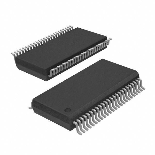
| 描述 | IC SWITCH BUS 16BIT FET 48-SSOP数字总线开关 IC 16-Bit FET Bus Switch |
| 产品分类 | |
| 品牌 | Texas Instruments |
| 产品手册 | |
| 产品图片 |
|
| rohs | 符合RoHS无铅 / 符合限制有害物质指令(RoHS)规范要求 |
| 产品系列 | 开关 IC,数字总线开关 IC,Texas Instruments SN74CB3Q16244DLR74CB |
| 数据手册 | |
| 产品型号 | SN74CB3Q16244DLR |
| 产品目录页面 | |
| 产品种类 | 数字总线开关 IC |
| 传播延迟时间 | 0.18 ns |
| 供应商器件封装 | 48-SSOP |
| 其它名称 | 296-19116-1 |
| 包装 | 剪切带 (CT) |
| 单位重量 | 600.300 mg |
| 商标 | Texas Instruments |
| 安装类型 | 表面贴装 |
| 安装风格 | SMD/SMT |
| 导通电阻—最大值 | 10 Ohms |
| 封装 | Reel |
| 封装/外壳 | 48-BSSOP(0.295",7.50mm 宽) |
| 封装/箱体 | SSOP-48 |
| 工作温度 | -40°C ~ 85°C |
| 工厂包装数量 | 1000 |
| 开关数量 | 16 |
| 技术 | CB3Q |
| 最大工作温度 | + 85 C |
| 最小工作温度 | - 40 C |
| 标准包装 | 1 |
| 独立电路 | 4 |
| 电压-电源 | 2.3 V ~ 3.6 V |
| 电压源 | 单电源 |
| 电流-输出高,低 | - |
| 电源电压-最大 | 3.6 V |
| 电源电压-最小 | 2.3 V |
| 电源电流 | 1 mA |
| 电路 | 4 x 1:1 |
| 类型 | FET 总线开关 |
| 系列 | SN74CB3Q16244 |
| 逻辑系列 | CB3Q |


- 商务部:美国ITC正式对集成电路等产品启动337调查
- 曝三星4nm工艺存在良率问题 高通将骁龙8 Gen1或转产台积电
- 太阳诱电将投资9.5亿元在常州建新厂生产MLCC 预计2023年完工
- 英特尔发布欧洲新工厂建设计划 深化IDM 2.0 战略
- 台积电先进制程称霸业界 有大客户加持明年业绩稳了
- 达到5530亿美元!SIA预计今年全球半导体销售额将创下新高
- 英特尔拟将自动驾驶子公司Mobileye上市 估值或超500亿美元
- 三星加码芯片和SET,合并消费电子和移动部门,撤换高东真等 CEO
- 三星电子宣布重大人事变动 还合并消费电子和移动部门
- 海关总署:前11个月进口集成电路产品价值2.52万亿元 增长14.8%


PDF Datasheet 数据手册内容提取
Product Sample & Technical Tools & Support & Folder Buy Documents Software Community SN74CB3Q16244 SCDS168A–MAY2004–REVISEDSEPTEMBER2015 SN74CB3Q16244 16-Bit FET Bus Switch 2.5-V – 3.3-V Low-Voltage High-Bandwidth Bus Switch 1 Features 2 Applications • High-BandwidthDataPath(Upto500MHz)(1) • IPPhones:WiredandWireless 1 • 5-VTolerantI/OsWithDevicePoweredUpor • OpticalModules PoweredDown • OpticalNetworking:VideoOverFiberandEPON • LowandFlatON-StateResistance(ron) • PrivateBranchExchange(PBX) CharacteristicsOverOperatingRange • WiMAXandWirelessInfrastructureEquipment (r =5ΩTypical) on • Rail-to-RailSwitchingonDataI/OPorts 3 Description – 0to5-VSwitchingWith3.3-VV The SN74CB3Q16244 device is a high-bandwidth CC – 0to3.3-VSwitchingWith2.5-VV FET bus switch using a charge pump to elevate the CC gate voltage of the pass transistor, providing a low • BidirectionalDataFlowWithNear-Zero and flat ON-state resistance (r ). The low and flat PropagationDelay on ON-state resistance allows for minimal propagation • LowInputandOutputCapacitanceMinimizes delay and supports rail-to-rail switching on the data LoadingandSignalDistortion input/output (I/O) ports. The SN74CB3Q16244 device (C =4pFTypical) also features low data I/O capacitance to minimize io(OFF) capacitive loading and signal distortion on the data • FastSwitchingFrequency(f =20MHz OE bus. Specifically designed to support high-bandwidth Maximum) applications, the SN74CB3Q16244 device provides • DataandControlInputsProvideUndershoot an optimized interface solution ideally suited for ClampDiodes broadband communications, networking, and data- • LowPowerConsumption(I =1mATypical) intensivecomputingsystems. CC • V OperatingRangeFrom2.3Vto3.6V CC DeviceInformation(1) • DataI/OsSupport0to5-VSignalingLevels PARTNUMBER PACKAGE BODYSIZE(NOM) (0.8V,1.2V,1.5V,1.8V,2.5V,3.3V,5V) SN74CB3Q16244DGG TSSOP(48) 12.50mm×6.10mm • ControlInputsCanBeDrivenbyTTLor SN74CB3Q16244DGV TVSOP(48) 9.70mm×4.40mm 5-Vand3.3-VCMOSOutputs SN74CB3Q16244DL SSOP(48) 15.88mm×7.49mm • I SupportsPartial-Power-DownModeOperation off (1) For all available packages, see the orderable addendum at • Latch-UpPerformanceExceeds100mA theendofthedatasheet. PerJESD78,ClassII • ESDPerformanceTestedPerJESD22 LogicDiagram(PositiveLogic) – 2000-VHumanBodyModel 47 2 41 8 (A114-B,ClassII) 1A1 SW 1B1 2A1 SW 2B1 – 1000-VCharged-DeviceModel(C101) 43 6 37 12 1A4 SW 1B4 2A4 SW 2B4 • SupportsBothDigitalandAnalogApplications 1 48 (1) Foradditionalinformationregardingtheperformance 1OE 2OE characteristicsoftheCB3Qfamily,refertotheTIapplication reportCBT-C,CB3T,andCB3QSignal-SwitchFamilies, (SCDA008). 3A1 36 SW 13 3B1 4A1 30 SW 19 4B1 32 17 26 23 3A4 SW 3B4 4A4 SW 4B4 25 24 3OE 4OE 1 An IMPORTANT NOTICE at the end of this data sheet addresses availability, warranty, changes, use in safety-critical applications, intellectualpropertymattersandotherimportantdisclaimers.PRODUCTIONDATA.
SN74CB3Q16244 SCDS168A–MAY2004–REVISEDSEPTEMBER2015 www.ti.com Table of Contents 1 Features.................................................................. 1 9.2 FunctionalBlockDiagram.........................................9 2 Applications........................................................... 1 9.3 FeatureDescription.................................................10 3 Description............................................................. 1 9.4 DeviceFunctionalModes........................................10 4 RevisionHistory..................................................... 2 10 ApplicationandImplementation........................ 11 10.1 ApplicationInformation..........................................11 5 Descriptioncontinued........................................... 3 10.2 TypicalApplication ...............................................11 6 PinConfigurationandFunctions......................... 4 11 PowerSupplyRecommendations..................... 12 7 Specifications......................................................... 5 12 Layout................................................................... 13 7.1 AbsoluteMaximumRatings .....................................5 12.1 LayoutGuidelines.................................................13 7.2 ESDRatings..............................................................5 12.2 LayoutExample....................................................13 7.3 RecommendedOperatingConditions......................5 13 DeviceandDocumentationSupport................. 14 7.4 ThermalInformation..................................................5 7.5 ElectricalCharacteristics..........................................6 13.1 DocumentationSupport........................................14 7.6 SwitchingCharacteristics..........................................6 13.2 CommunityResources..........................................14 7.7 TypicalCharacteristics..............................................7 13.3 Trademarks...........................................................14 13.4 ElectrostaticDischargeCaution............................14 8 ParameterMeasurementInformation..................8 13.5 Glossary................................................................14 9 DetailedDescription.............................................. 9 14 Mechanical,Packaging,andOrderable 9.1 Overview...................................................................9 Information........................................................... 14 4 Revision History NOTE:Pagenumbersforpreviousrevisionsmaydifferfrompagenumbersinthecurrentversion. ChangesfromRevisionA(March2005)toRevisionB Page • AddedApplications,DeviceInformationtable,PinConfigurationandFunctionssection,ESDRatingstable,Feature Descriptionsection,DeviceFunctionalModes,ApplicationandImplementationsection,PowerSupply Recommendationssection,Layoutsection,DeviceandDocumentationSupportsection,andMechanical, Packaging,andOrderableInformationsection ..................................................................................................................... 1 • RemovedOrderingInformationtable. ................................................................................................................................... 1 2 SubmitDocumentationFeedback Copyright©2004–2015,TexasInstrumentsIncorporated ProductFolderLinks:SN74CB3Q16244
SN74CB3Q16244 www.ti.com SCDS168A–MAY2004–REVISEDSEPTEMBER2015 5 Description continued The SN74CB3Q16244 device is organized as four 4-bit bus switches with separate output-enable (1OE, 2OE, 3OE, 4OE) inputs. It can be used as four 4-bit bus switches, two 8-bit bus switches, or one 16-bit bus switch. When OE is low, the associated 4-bit bus switch is ON, and the A port is connected to the B port, allowing bidirectional data flow between ports. When OE is high, the associated 4-bit bus switch is OFF, and a high- impedancestateexistsbetweentheAandBports. This device is fully specified for partial-power-down applications using I . The I circuitry prevents damaging off off currentbackflowthroughthedevicewhenitispowereddown.Thedevicehasisolationduringpoweroff. To ensure the high-impedance state during power up or power down, OE should be tied to V through a pullup CC resistor;theminimumvalueoftheresistorisdeterminedbythecurrent-sinkingcapabilityofthedriver. Copyright©2004–2015,TexasInstrumentsIncorporated SubmitDocumentationFeedback 3 ProductFolderLinks:SN74CB3Q16244
SN74CB3Q16244 SCDS168A–MAY2004–REVISEDSEPTEMBER2015 www.ti.com 6 Pin Configuration and Functions DGG,DGV,orDLPackage 48-PinTSSOP,TVSOP,orSSOP TopView 1OE 1 48 2OE 1B1 2 47 1A1 1B2 3 46 1A2 GND 4 45 GND 1B3 5 44 1A3 1B4 6 43 1A4 VCC 7 42 VCC 2B1 8 41 2A1 2B2 9 40 2A2 GND 10 39 GND 2B3 11 38 2A3 2B4 12 37 2A4 3B1 13 36 3A1 3B2 14 35 3A2 GND 15 34 GND 3B3 16 33 3A3 3B4 17 32 3A4 VCC 18 31 VCC 4B1 19 30 4A1 4B2 20 29 4A2 GND 21 28 GND 4B3 22 27 4A3 4B4 23 26 4A4 4OE 24 25 3OE PinFunctions PIN I/O DESCRIPTION NAME NO. 1A1,1A2 47,46 I/O Bidirectionalsignaltobeswitched 1A3,1A4 44,43 1B1,1B2 2,3 I/O Bidirectionalsignaltobeswitched 1B3,1B4 5,6 SwitchOutputEnabletoconnectpins1A1,1A2,1A3,1A4to1B1,1B2,1B3,1B4 1OE 1 I (ActiveLow:L=ON,H=OFF) 2A1,2A2 41,40 I/O Bidirectionalsignaltobeswitched 2A3,2A4 38,37 2B1,2B2 8,9 I/O Bidirectionalsignaltobeswitched 2B3,2B4 11,12 SwitchOutputEnabletoconnectpins2A1,2A2,2A3,2A4to2B1,2B2,2B3,2B4 2OE 48 I (ActiveLow:L=ON,H=OFF) 3A1,3A2 36,35 I/O Bidirectionalsignaltobeswitched 3A3,3A4 33,32 3B1,3B2 13,14 I/O Bidirectionalsignaltobeswitched 3B3,3B4 16,17 SwitchOutputEnabletoconnectpins3A1,3A2,3A3,3A4to3B1,3B2,3B3,3B4 3OE 25 I (ActiveLow:L=ON,H=OFF) 4A1,4A2 30,29 I/O Bidirectionalsignaltobeswitched 4A3,4A4 27,26 4B1,4B2 19,20 I/O Bidirectionalsignaltobeswitched 4B3,4B4 22,23 SwitchOutputEnabletoconnectpins4A1,4A2,4A3,4A4to4B1,4B2,4B3,4B4 4OE 24 I (ActiveLow:L=ON,H=OFF) V 7,18,31,42 — PowerSupply CC 4,10,15,21 GND — Ground 28,34,39,45 4 SubmitDocumentationFeedback Copyright©2004–2015,TexasInstrumentsIncorporated ProductFolderLinks:SN74CB3Q16244
SN74CB3Q16244 www.ti.com SCDS168A–MAY2004–REVISEDSEPTEMBER2015 7 Specifications 7.1 Absolute Maximum Ratings overoperatingfree-airtemperaturerange(unlessotherwisenoted)(1) MIN MAX UNIT V Supplyvoltage(2) –0.5 4.6 V CC V Controlinputvoltage(2)(3) –0.5 7 V IN V SwitchI/Ovoltage(2)(3)(4) –0.5 7 V I/O I Controlinputclampcurrent V <0 –50 mA IK IN I I/Oportclampcurrent V <0 –50 mA I/OK I/O I ON-stateswitchcurrent(5) ±64 mA I/O ContinuouscurrentthroughV orGND ±100 mA CC T Junctiontemperature 150 J °C T Storagetemperature –65 150 stg (1) StressesbeyondthoselistedunderAbsoluteMaximumRatingsmaycausepermanentdamagetothedevice.Thesearestressratings only,andfunctionaloperationofthedeviceattheseoranyotherconditionsbeyondthoseindicatedunderRecommendedOperating Conditionsisnotimplied.Exposuretoabsolute-maximum-ratedconditionsforextendedperiodsmayaffectdevicereliability. (2) Allvoltagesarewithrespecttoground,unlessotherwisespecified. (3) Theinputandoutputvoltageratingsmaybeexceedediftheinputandoutputclamp-currentratingsareobserved. (4) V andV areusedtodenotespecificconditionsforV . I O I/O (5) I andI areusedtodenotespecificconditionsforI . I O I/O 7.2 ESD Ratings VALUE UNIT Humanbodymodel(HBM),perANSI/ESDA/JEDECJS-001(1) +2000 V(ESD) Electrostaticdischarge Charged-devicemodel(CDM),perJEDECspecificationJESD22- V C101(2) +1000 (1) JEDECdocumentJEP155statesthat500-VHBMallowssafemanufacturingwithastandardESDcontrolprocess. (2) JEDECdocumentJEP157statesthat250-VCDMallowssafemanufacturingwithastandardESDcontrolprocess. 7.3 Recommended Operating Conditions overoperatingfree-airtemperaturerange(unlessotherwisenoted)(1) MIN MAX UNIT V Supplyvoltage 2.3 3.6 V CC V =2.3Vto2.7V 1.7 5.5 CC V High-levelcontrolinputvoltage V IH V =2.7Vto3.6V 2 5.5 CC V =2.3Vto2.7V 0 0.7 CC V Low-levelcontrolinputvoltage V IL V =2.7Vto3.6V 0 0.8 CC V Datainput/outputvoltage 0 5.5 V I/O T Operatingfree-airtemperature –40 85 °C A (1) AllunusedcontrolinputsofthedevicemustbeheldatV orGNDtoensureproperdeviceoperation.RefertotheTIapplicationreport, CC ImplicationsofSloworFloatingCMOSInputs(SCBA004). 7.4 Thermal Information SN74CB3Q16244 THERMALMETRIC(1) DGG(TSSOP) DGV(TVSOP) DL(SSOP) UNIT 48PINS 48PINS 48PINS R Junction-to-ambientthermalresistance 70 58 63 °C/W θJA (1) Formoreinformationabouttraditionalandnewthermalmetrics,seetheSemiconductorandICPackageThermalMetricsapplication report,SPRA953. Copyright©2004–2015,TexasInstrumentsIncorporated SubmitDocumentationFeedback 5 ProductFolderLinks:SN74CB3Q16244
SN74CB3Q16244 SCDS168A–MAY2004–REVISEDSEPTEMBER2015 www.ti.com 7.5 Electrical Characteristics overrecommendedoperatingfree-airtemperaturerange(unlessotherwisenoted)(1) PARAMETER TESTCONDITIONS MIN TYP(2) MAX UNIT V V =3.6V, I =–18mA –1.8 V IK CC I I Controlinputs V =3.6V, V =0to5.5V ±1 µA IN CC IN I (3) V =3.6V, VO=0to5.5V, SwitchOFF, ±1 µA OZ CC V =0, V =V orGND I IN CC I V =0, V =0to5.5V, V =0 1 µA off CC O I I =0, I V =3.6V, I/O V =V orGND 1 2 mA CC CC SwitchONorOFF, IN CC ΔI (4) Controlinputs V =3.6V, Oneinputat3V, OtherinputsatV orGND 30 µA CC CC CC I (5) Percontrol V =3.6V, AandBportsopen, 0.15 0.25 mA/ CCD input CC Controlinputswitchingat50%dutycycle MHz C Controlinputs V =3.3V, V =5.5V,3.3V,or0 3.5 5 pF in CC IN SwitchOFF, C V =3.3V, V =5.5V,3.3V,or0 4 6 pF io(OFF) CC V =V orGND, I/O IN CC SwitchON, C V =3.3V, V =5.5V,3.3V,or0 10 13 pF io(ON) CC V =V orGND, I/O IN CC VCC=2.3V, VI=0, IO=30mA 6 8 r (6) TYPatVCC=2.5V VI=1.7V, IO=–15mA 5 10 Ω on V =0, I =30mA 6 8 I O V =3V CC V =2.4V, I =–15mA 5 9 I O (1) V andI refertocontrolinputs.V,V ,I,andI refertodatapins. IN IN I O I O (2) AlltypicalvaluesareatV =3.3V(unlessotherwisenoted),T =25°C. CC A (3) ForI/Oports,theparameterI includestheinputleakagecurrent. OZ (4) ThisistheincreaseinsupplycurrentforeachinputthatisatthespecifiedTTLvoltagelevel,ratherthanV orGND. CC (5) Thisparameterspecifiesthedynamicpower-supplycurrentassociatedwiththeoperatingfrequencyofasinglecontrolinput (seeFigure1). (6) MeasuredbythevoltagedropbetweentheAandBterminalsattheindicatedcurrentthroughtheswitch.ON-stateresistanceis determinedbythelowerofthevoltagesofthetwo(AorB)terminals. 7.6 Switching Characteristics overrecommendedoperatingfree-airtemperaturerange(unlessotherwisenoted)(seeFigure2) V =2.5V V =3.3V CC CC PARAMETER FROM TO ±0.2V ±0.3V UNIT (INPUT) (OUTPUT) MIN MAX MIN MAX f (1) OE AorB 10 20 MHz OE t (2) AorB BorA 0.18 0.3 ns pd t OE AorB 1.5 8 1.5 7 ns en t OE AorB 1 8 1 7 ns dis (1) Maximumswitchingfrequencyforcontrolinput(V >V ,V =5V,R ≥1MΩ,C =0) O CC I L L (2) ThepropagationdelayisthecalculatedRCtimeconstantofthetypicalON-stateresistanceoftheswitchandthespecifiedload capacitance,whendrivenbyanidealvoltagesource(zerooutputimpedance). 6 SubmitDocumentationFeedback Copyright©2004–2015,TexasInstrumentsIncorporated ProductFolderLinks:SN74CB3Q16244
SN74CB3Q16244 www.ti.com SCDS168A–MAY2004–REVISEDSEPTEMBER2015 7.7 Typical Characteristics 12 VCC = 3.3 V 10 TA = 25°C A and B Ports Open 8 A m − 6 C C I 4 One OE Switching 2 0 0 2 4 6 8 10 12 14 16 18 20 OE Switching Frequency − MHz Figure1.TypicalI vsOESwitchingFrequency CC Copyright©2004–2015,TexasInstrumentsIncorporated SubmitDocumentationFeedback 7 ProductFolderLinks:SN74CB3Q16244
SN74CB3Q16244 SCDS168A–MAY2004–REVISEDSEPTEMBER2015 www.ti.com 8 Parameter Measurement Information VCC Input Generator VIN 50 Ω VG1 50 Ω TEST CIRCUIT DUT 2 × VCC Input Generator S1 VI VO RL Open 50 Ω GND VG2 50 Ω CL RL (see Note A) TEST VCC S1 RL VI CL V∆ tpd(s) 2.5 V ± 0.2 V Open 500 Ω VCC or GND 30 pF 3.3 V ± 0.3 V Open 500 Ω VCC or GND 50 pF tPLZ/tPZL 23..53 VV ±± 00..23 VV 22 ×× VVCCCC 550000 ΩΩ GGNNDD 3500 ppFF 00.1.35 V V tPHZ/tPZH 23..53 VV ±± 00..23 VV GGNNDD 550000 ΩΩ VVCCCC 3500 ppFF 00.1.35 V V Output VCC Control VCC/2 VCC/2 (VIN) 0 V tPZL tPLZ Output Output VCC Waveform 1 VCC Control VCC/2 VCC/2 S1 at 2 × VCC VCC/2 VOL + VD (VIN) 0 V (see Note B) VOL tPZH tPHZ tPLH tPHL Output VOH VOH Waveform 2 VOH − VD Output VCC/2 VCC/2 S1 at GND VCC/2 VOL (see Note B) 0 V VOLTAGE WAVEFORMS VOLTAGE WAVEFORMS PROPAGATION DELAY TIMES (tpd(s)) ENABLE AND DISABLE TIMES NOTES: A. CL includes probe and jig capacitance. B. Waveform 1 is for an output with internal conditions such that the output is low, except when disabled by the output control. Waveform 2 is for an output with internal conditions such that the output is high, except when disabled by the output control. C. All input pulses are supplied by generators having the following characteristics: PRR ≤ 10 MHz, ZO = 50 W , tr ≤ 2.5 ns, tf ≤ 2.5 ns. D. The outputs are measured one at a time, with one transition per measurement. E. tPLZ and tPHZ are the same as tdis. F. tPZL and tPZH are the same as ten. G. tPLH and tPHL are the same as tpd(s). The tpd propagation delay is the calculated RC time constant of the typical ON-state resistance of the switch and the specified load capacitance, when driven by an ideal voltage source (zero output impedance). H. All parameters and waveforms are not applicable to all devices. Figure2. TestCircuitandVoltageWaveforms 8 SubmitDocumentationFeedback Copyright©2004–2015,TexasInstrumentsIncorporated ProductFolderLinks:SN74CB3Q16244
SN74CB3Q16244 www.ti.com SCDS168A–MAY2004–REVISEDSEPTEMBER2015 9 Detailed Description 9.1 Overview The SN74CB3Q16244 is part of the CB3Q family of switches. The SN74CB3Q16244 is a 16-bit FET bus switch inwhich4OutputEnablepinseachcontrolasetof4switchestotaling16switches. A B VCC Charge Pump EN(1) (1) EN is the internal enable signal applied to the switch. Figure3. SimplifiedSchematic,EachFETSwitch(SW) 9.2 Functional Block Diagram 47 2 41 8 1A1 SW 1B1 2A1 SW 2B1 43 6 37 12 1A4 SW 1B4 2A4 SW 2B4 1 48 1OE 2OE 36 13 30 19 3A1 SW 3B1 4A1 SW 4B1 32 17 26 23 3A4 SW 3B4 4A4 SW 4B4 25 24 3OE 4OE Figure4. LogicDiagram(PositiveLogic) Copyright©2004–2015,TexasInstrumentsIncorporated SubmitDocumentationFeedback 9 ProductFolderLinks:SN74CB3Q16244
SN74CB3Q16244 SCDS168A–MAY2004–REVISEDSEPTEMBER2015 www.ti.com 9.3 Feature Description TheSN74CB3Q16244devicehasahigh-bandwidthdatapath(upto500MHz)andhas5-VtolerantI/Oswiththe device powered up or powered down. It also has low and flat ON-state resistance (r ) characteristics over on operatingrange(r =5 ΩTypical) on This device also has rail-to-rail switching on data I/O ports for 0 to 5-V switching with 3.3-V V and 0 to 3.3-V CC switching with 2.5-V V as well as bidirectional data flow with near-zero propagation delay and low input and CC outputcapacitancethatminimizesloadingandsignaldistortion(C =4pFTypical) io(OFF) The SN74CB3Q16244 also provides a fast switching frequency (f = 20 MHz Maximum) with data and control OE inputsthatprovideundershootclampdiodesaswellaslowpowerconsumption(I =1mATypical) CC The V operating range is from 2.3 V to 3.6 V and the data I/Os support 0 to 5-V signal levels of (0.8-V, 1.2-V, CC 1.5-V,1.8-V,2.5-V,3.3-V,5-V) The control inputs can be driven by TTL or 5-V and 3.3-V CMOS outputs, and I supports partial-power-down off modeoperation. 9.4 Device Functional Modes Table1liststhefunctionalmodesoftheSN74CB3Q16244. Table1.FunctionTable (EachMultiplexer/Demultiplexer) INPUT INPUT/OUTPUT FUNCTION OE A L B Aport=Bport H Z Disconnect 10 SubmitDocumentationFeedback Copyright©2004–2015,TexasInstrumentsIncorporated ProductFolderLinks:SN74CB3Q16244
SN74CB3Q16244 www.ti.com SCDS168A–MAY2004–REVISEDSEPTEMBER2015 10 Application and Implementation NOTE Information in the following applications sections is not part of the TI component specification, and TI does not warrant its accuracy or completeness. TI’s customers are responsible for determining suitability of components for their purposes. Customers should validateandtesttheirdesignimplementationtoconfirmsystemfunctionality. 10.1 Application Information TheSN74CB3Q16244devicecanbeusedtocontrolupto16bitswith4channelssimultaneously. 10.2 Typical Application The application shown in Figure 5 is a 16-bit bus being controlled. The OE pins are used to control the chip from the bus controller. This is a generic example and can apply to many situations. If an application requires fewer than16bits,ensurethattheAsideistiedeitherhighorlowonunusedchannels. 1OE 1 1A1 47 ron 2 1B1 1A2 1B2 1A3 1B3 1A4 43 ron 6 1B4 2OE 48 2A1 41 ron 8 2B1 2A2 2B2 2A3 2B3 2A4 37 ron 12 2B4 16 16 Bus 3OE Device Controller 25 3A1 36 ron 13 3B1 3A2 3B2 3A3 3B3 3A4 32 ron 17 3B4 4OE 24 4A1 30 ron 19 4B1 4A2 4B2 4A3 4B3 4A4 26 ron 23 4B4 7 VCC 0.022 (cid:29)F 4, 10, 18 VCC 0.022 (cid:29)F GND 15, 21 28, 34, 31 VCC 0.022 (cid:29)F 39, 45 42 VCC 0.022 (cid:29)F Figure5. TypicalApplicationoftheSN74CB3Q16244 Copyright©2004–2015,TexasInstrumentsIncorporated SubmitDocumentationFeedback 11 ProductFolderLinks:SN74CB3Q16244
SN74CB3Q16244 SCDS168A–MAY2004–REVISEDSEPTEMBER2015 www.ti.com Typical Application (continued) 10.2.1 DesignRequirements A 0.022-µF bypass capacitor should be placed between each V pin and GND. Each capacitor must be placed CC ascloseaspossibletotheSN74CB3Q16244device. 10.2.2 DetailedDesignProcedure 1. Recommendedinputconditions: – Forspecifiedhighandlowlevels,seeV andV inRecommendedOperatingConditions IH IL – Inputsandoutputsareovervoltagetolerant,whichallowsthemtogoashighas5.5VatanyvalidV CC 2. Recommendedoutputconditions: – Loadcurrentsmustnotexceed ±64mAperchannel 3. Frequencyselectioncriterion: – Addedtraceresistanceorcapacitancecanreducemaximumfrequencycapability;uselayoutpracticesas directedinLayout 10.2.3 ApplicationCurve 16 (cid:1)– 14 VTAC C= =2 53°.C3 V ce 12 IO = −15 mA n a st 10 si Re 8 e at 6 St N- 4 O – n 2 o r 0 0.0 0.5 1.0 1.5 2.0 2.5 3.0 3.5 4.0 4.5 5.0 VI − V Figure6.Typicalr vsV on I 11 Power Supply Recommendations The power supply can be any voltage between the minimum and maximum supply voltage rating listed in the AbsoluteMaximumRatingstable. Each V terminal should have a good bypass capacitor to prevent power disturbance. For devices with a single CC supply, a 0.1-μF bypass capacitor is recommended. If multiple pins are labeled V , then a 0.01-μF or 0.022-μF CC capacitor is recommended for each V because the V pins are tied together internally. For devices with dual- CC CC supply pins operating at different voltages, for example V and V , a 0.1-µF bypass capacitor is recommended CC DD foreachsupplypin.Torejectdifferentfrequenciesofnoise,usemultiplebypasscapacitorsinparallel.Capacitors withvaluesof0.1 μFand1 μFarecommonlyusedinparallel.Thebypasscapacitormustbeinstalledascloseto thepowerterminalaspossibleforbestresults. 12 SubmitDocumentationFeedback Copyright©2004–2015,TexasInstrumentsIncorporated ProductFolderLinks:SN74CB3Q16244
SN74CB3Q16244 www.ti.com SCDS168A–MAY2004–REVISEDSEPTEMBER2015 12 Layout 12.1 Layout Guidelines Reflections and matching are closely related to the loop antenna theory but are different enough to be discussed separately from the theory. When a PCB trace turns a corner at a 90° angle, a reflection can occur. A reflection occurs primarily because of the change of width of the trace. At the apex of the turn, the trace width increases to 1.414 times the width. This increase upsets the transmission-line characteristics, especially the distributed capacitance and self-inductance of the trace, which results in the reflection. Not all PCB traces can be straight; therefore, some traces must turn corners. Figure 7 shows progressively better techniques of rounding corners. Onlythelastexample(BEST)maintainsconstanttracewidthandminimizesreflections. 12.2 Layout Example WORST BETTER BEST W 2 1W min. W Figure7. TraceExample Copyright©2004–2015,TexasInstrumentsIncorporated SubmitDocumentationFeedback 13 ProductFolderLinks:SN74CB3Q16244
SN74CB3Q16244 SCDS168A–MAY2004–REVISEDSEPTEMBER2015 www.ti.com 13 Device and Documentation Support 13.1 Documentation Support 13.1.1 RelatedDocumentation Forrelateddocumentationseethefollowing: • CBT-C,CB3T,andCB3QSignal-SwitchFamilies,SCDA008 • ImplicationsofSloworFloatingCMOSInputs,SCBA004 • SelectingtheRightTexasInstrumentsSignalSwitch,SZZA030 13.2 Community Resources The following links connect to TI community resources. Linked contents are provided "AS IS" by the respective contributors. They do not constitute TI specifications and do not necessarily reflect TI's views; see TI's Terms of Use. TIE2E™OnlineCommunity TI'sEngineer-to-Engineer(E2E)Community.Createdtofostercollaboration amongengineers.Ate2e.ti.com,youcanaskquestions,shareknowledge,exploreideasandhelp solveproblemswithfellowengineers. DesignSupport TI'sDesignSupport QuicklyfindhelpfulE2Eforumsalongwithdesignsupporttoolsand contactinformationfortechnicalsupport. 13.3 Trademarks E2EisatrademarkofTexasInstruments. Allothertrademarksarethepropertyoftheirrespectiveowners. 13.4 Electrostatic Discharge Caution Thesedeviceshavelimitedbuilt-inESDprotection.Theleadsshouldbeshortedtogetherorthedeviceplacedinconductivefoam duringstorageorhandlingtopreventelectrostaticdamagetotheMOSgates. 13.5 Glossary SLYZ022—TIGlossary. Thisglossarylistsandexplainsterms,acronyms,anddefinitions. 14 Mechanical, Packaging, and Orderable Information The following pages include mechanical, packaging, and orderable information. This information is the most current data available for the designated devices. This data is subject to change without notice and revision of thisdocument.Forbrowser-basedversionsofthisdatasheet,refertotheleft-handnavigation. 14 SubmitDocumentationFeedback Copyright©2004–2015,TexasInstrumentsIncorporated ProductFolderLinks:SN74CB3Q16244
PACKAGE OPTION ADDENDUM www.ti.com 6-Feb-2020 PACKAGING INFORMATION Orderable Device Status Package Type Package Pins Package Eco Plan Lead/Ball Finish MSL Peak Temp Op Temp (°C) Device Marking Samples (1) Drawing Qty (2) (6) (3) (4/5) 74CB3Q16244DGGRG4 ACTIVE TSSOP DGG 48 2000 Green (RoHS NIPDAU Level-1-260C-UNLIM -40 to 85 CB3Q16244 & no Sb/Br) SN74CB3Q16244DGGR ACTIVE TSSOP DGG 48 2000 Green (RoHS NIPDAU Level-1-260C-UNLIM -40 to 85 CB3Q16244 & no Sb/Br) SN74CB3Q16244DGVR ACTIVE TVSOP DGV 48 2000 Green (RoHS NIPDAU Level-1-260C-UNLIM -40 to 85 BW244 & no Sb/Br) SN74CB3Q16244DL ACTIVE SSOP DL 48 25 Green (RoHS NIPDAU Level-1-260C-UNLIM -40 to 85 CB3Q16244 & no Sb/Br) SN74CB3Q16244DLR ACTIVE SSOP DL 48 1000 Green (RoHS NIPDAU Level-1-260C-UNLIM -40 to 85 CB3Q16244 & no Sb/Br) (1) The marketing status values are defined as follows: ACTIVE: Product device recommended for new designs. LIFEBUY: TI has announced that the device will be discontinued, and a lifetime-buy period is in effect. NRND: Not recommended for new designs. Device is in production to support existing customers, but TI does not recommend using this part in a new design. PREVIEW: Device has been announced but is not in production. Samples may or may not be available. OBSOLETE: TI has discontinued the production of the device. (2) RoHS: TI defines "RoHS" to mean semiconductor products that are compliant with the current EU RoHS requirements for all 10 RoHS substances, including the requirement that RoHS substance do not exceed 0.1% by weight in homogeneous materials. Where designed to be soldered at high temperatures, "RoHS" products are suitable for use in specified lead-free processes. TI may reference these types of products as "Pb-Free". RoHS Exempt: TI defines "RoHS Exempt" to mean products that contain lead but are compliant with EU RoHS pursuant to a specific EU RoHS exemption. Green: TI defines "Green" to mean the content of Chlorine (Cl) and Bromine (Br) based flame retardants meet JS709B low halogen requirements of <=1000ppm threshold. Antimony trioxide based flame retardants must also meet the <=1000ppm threshold requirement. (3) MSL, Peak Temp. - The Moisture Sensitivity Level rating according to the JEDEC industry standard classifications, and peak solder temperature. (4) There may be additional marking, which relates to the logo, the lot trace code information, or the environmental category on the device. (5) Multiple Device Markings will be inside parentheses. Only one Device Marking contained in parentheses and separated by a "~" will appear on a device. If a line is indented then it is a continuation of the previous line and the two combined represent the entire Device Marking for that device. (6) Lead/Ball Finish - Orderable Devices may have multiple material finish options. Finish options are separated by a vertical ruled line. Lead/Ball Finish values may wrap to two lines if the finish value exceeds the maximum column width. Addendum-Page 1
PACKAGE OPTION ADDENDUM www.ti.com 6-Feb-2020 Important Information and Disclaimer:The information provided on this page represents TI's knowledge and belief as of the date that it is provided. TI bases its knowledge and belief on information provided by third parties, and makes no representation or warranty as to the accuracy of such information. Efforts are underway to better integrate information from third parties. TI has taken and continues to take reasonable steps to provide representative and accurate information but may not have conducted destructive testing or chemical analysis on incoming materials and chemicals. TI and TI suppliers consider certain information to be proprietary, and thus CAS numbers and other limited information may not be available for release. In no event shall TI's liability arising out of such information exceed the total purchase price of the TI part(s) at issue in this document sold by TI to Customer on an annual basis. Addendum-Page 2
PACKAGE MATERIALS INFORMATION www.ti.com 11-Mar-2017 TAPE AND REEL INFORMATION *Alldimensionsarenominal Device Package Package Pins SPQ Reel Reel A0 B0 K0 P1 W Pin1 Type Drawing Diameter Width (mm) (mm) (mm) (mm) (mm) Quadrant (mm) W1(mm) SN74CB3Q16244DGGR TSSOP DGG 48 2000 330.0 24.4 8.6 13.0 1.8 12.0 24.0 Q1 SN74CB3Q16244DGVR TVSOP DGV 48 2000 330.0 16.4 7.1 10.2 1.6 12.0 16.0 Q1 SN74CB3Q16244DLR SSOP DL 48 1000 330.0 32.4 11.35 16.2 3.1 16.0 32.0 Q1 PackMaterials-Page1
PACKAGE MATERIALS INFORMATION www.ti.com 11-Mar-2017 *Alldimensionsarenominal Device PackageType PackageDrawing Pins SPQ Length(mm) Width(mm) Height(mm) SN74CB3Q16244DGGR TSSOP DGG 48 2000 367.0 367.0 45.0 SN74CB3Q16244DGVR TVSOP DGV 48 2000 367.0 367.0 38.0 SN74CB3Q16244DLR SSOP DL 48 1000 367.0 367.0 55.0 PackMaterials-Page2
None
MECHANICAL DATA MPDS006C – FEBRUARY 1996 – REVISED AUGUST 2000 DGV (R-PDSO-G**) PLASTIC SMALL-OUTLINE 24 PINS SHOWN 0,23 0,40 0,07 M 0,13 24 13 0,16 NOM 4,50 6,60 4,30 6,20 Gage Plane 0,25 0°–(cid:1)8° 0,75 1 12 0,50 A Seating Plane 0,15 1,20 MAX 0,08 0,05 PINS ** 14 16 20 24 38 48 56 DIM A MAX 3,70 3,70 5,10 5,10 7,90 9,80 11,40 A MIN 3,50 3,50 4,90 4,90 7,70 9,60 11,20 4073251/E 08/00 NOTES: A. All linear dimensions are in millimeters. B. This drawing is subject to change without notice. C. Body dimensions do not include mold flash or protrusion, not to exceed 0,15 per side. D. Falls within JEDEC: 24/48 Pins – MO-153 14/16/20/56 Pins – MO-194 • POST OFFICE BOX 655303 DALLAS, TEXAS 75265
MECHANICAL DATA MTSS003D – JANUARY 1995 – REVISED JANUARY 1998 DGG (R-PDSO-G**) PLASTIC SMALL-OUTLINE PACKAGE 48 PINS SHOWN 0,27 0,50 0,08 M 0,17 48 25 6,20 8,30 6,00 7,90 0,15 NOM Gage Plane 0,25 1 24 0°–8° A 0,75 0,50 Seating Plane 0,15 1,20 MAX 0,10 0,05 PINS ** 48 56 64 DIM A MAX 12,60 14,10 17,10 A MIN 12,40 13,90 16,90 4040078/F 12/97 NOTES: A. All linear dimensions are in millimeters. B. This drawing is subject to change without notice. C. Body dimensions do not include mold protrusion not to exceed 0,15. D. Falls within JEDEC MO-153 • POST OFFICE BOX 655303 DALLAS, TEXAS 75265
IMPORTANTNOTICEANDDISCLAIMER TI PROVIDES TECHNICAL AND RELIABILITY DATA (INCLUDING DATASHEETS), DESIGN RESOURCES (INCLUDING REFERENCE DESIGNS), APPLICATION OR OTHER DESIGN ADVICE, WEB TOOLS, SAFETY INFORMATION, AND OTHER RESOURCES “AS IS” AND WITH ALL FAULTS, AND DISCLAIMS ALL WARRANTIES, EXPRESS AND IMPLIED, INCLUDING WITHOUT LIMITATION ANY IMPLIED WARRANTIES OF MERCHANTABILITY, FITNESS FOR A PARTICULAR PURPOSE OR NON-INFRINGEMENT OF THIRD PARTY INTELLECTUAL PROPERTY RIGHTS. These resources are intended for skilled developers designing with TI products. You are solely responsible for (1) selecting the appropriate TI products for your application, (2) designing, validating and testing your application, and (3) ensuring your application meets applicable standards, and any other safety, security, or other requirements. These resources are subject to change without notice. TI grants you permission to use these resources only for development of an application that uses the TI products described in the resource. Other reproduction and display of these resources is prohibited. No license is granted to any other TI intellectual property right or to any third party intellectual property right. TI disclaims responsibility for, and you will fully indemnify TI and its representatives against, any claims, damages, costs, losses, and liabilities arising out of your use of these resources. TI’s products are provided subject to TI’s Terms of Sale (www.ti.com/legal/termsofsale.html) or other applicable terms available either on ti.com or provided in conjunction with such TI products. TI’s provision of these resources does not expand or otherwise alter TI’s applicable warranties or warranty disclaimers for TI products. Mailing Address: Texas Instruments, Post Office Box 655303, Dallas, Texas 75265 Copyright © 2020, Texas Instruments Incorporated