ICGOO在线商城 > SN74AVCA406ZQCR
 Datasheet下载
- 型号: SN74AVCA406ZQCR
- 制造商: Texas Instruments
- 库位|库存: xxxx|xxxx
- 要求:
| 数量阶梯 | 香港交货 | 国内含税 |
| +xxxx | $xxxx | ¥xxxx |
查看当月历史价格
查看今年历史价格
SN74AVCA406ZQCR产品简介:
ICGOO电子元器件商城为您提供SN74AVCA406ZQCR由Texas Instruments设计生产,在icgoo商城现货销售,并且可以通过原厂、代理商等渠道进行代购。 提供SN74AVCA406ZQCR价格参考以及Texas InstrumentsSN74AVCA406ZQCR封装/规格参数等产品信息。 你可以下载SN74AVCA406ZQCR参考资料、Datasheet数据手册功能说明书, 资料中有SN74AVCA406ZQCR详细功能的应用电路图电压和使用方法及教程。
| 参数 | 数值 |
| 产品目录 | 集成电路 (IC) |
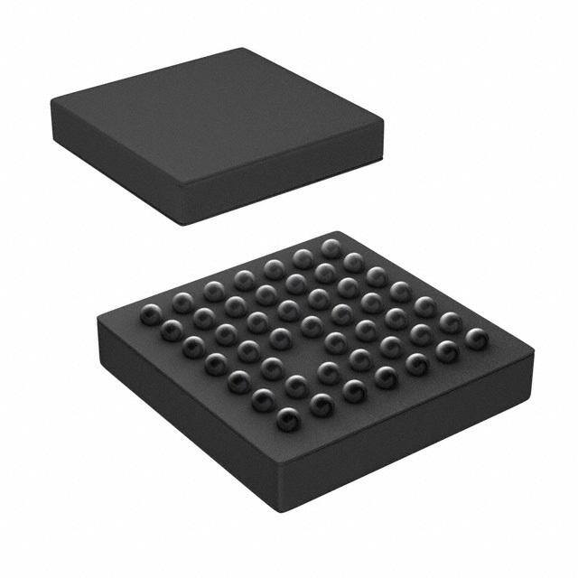
| 描述 | IC VOLT TRANSL SD MMC 48BGA |
| 产品分类 | 逻辑 - 变换器 |
| 品牌 | Texas Instruments |
| 数据手册 | |
| 产品图片 |
|
| 产品型号 | SN74AVCA406ZQCR |
| rohs | 无铅 / 符合限制有害物质指令(RoHS)规范要求 |
| 产品系列 | 74AVCA |
| 产品目录页面 | |
| 传播延迟(最大值) | - |
| 位数 | 4 |
| 供应商器件封装 | 48-BGA MICROSTAR JUNIOR(4x4) |
| 其它名称 | 296-17829-1 |
| 包装 | 剪切带 (CT) |
| 安装类型 | 表面贴装 |
| 封装/外壳 | 48-VFBGA |
| 工作温度 | -40°C ~ 85°C |
| 差分-输入:输出 | 无/无 |
| 数据速率 | - |
| 标准包装 | 1 |
| 电压-电源 | 1.4 V ~ 3.6 V |
| 输入类型 | 电压 |
| 输出/通道数 | 1 |
| 输出类型 | 电压 |
| 通道数 | 4 |
| 逻辑功能 | 变换器 |


PDF Datasheet 数据手册内容提取
SN74AVCA406 MMC, SD CARD, Memory Stick, SmartMedia, AND xD-Picture Card – 15-kV ESD-PROTECTED VOLTAGE-TRANSLATION TRANSCEIVER www.ti.com SCES615H–OCTOBER2004–REVISEDJANUARY2007 FEATURES • TransceiverforMemoryCardInterface • ESDProtectionforCard-SidePins(BPort) [MultiMediaCard(MMC),SecureDigital(SD), – – 15kV(– 12kVonPin14B)–IEC61000-4-2 MemoryStick™CompliantProducts, ESD,Air-GapDischarge SmartMediaCard,andxD-PictureCard™] – – 8kV–IEC61000-4-2ESD,Contact • ConfigurableI/OSwitchingLevelsWith Discharge Dual-SupplyPinsOperatingOverFull1.4-Vto • ESDProtectionforA-PortPins(TestedPer 3.6-VPower-SupplyRange JESD22)Exceeds • ForLow-PowerOperation,APortsArePlaced – 2000-VHuman-BodyModel(A114-B inHigh-ImpedanceStateWhenCard-Side – 1000-VCharged-DeviceModel(C101) SupplyVoltageIsSwitchedOff • Latch-UpPerformanceExceeds100mAPer xxxxxxx JESD78,ClassII DESCRIPTION/ORDERING INFORMATION The SN74AVCA406 is a transceiver for interfacing microprocessors with MultiMediaCards (MMCs), secure digital (SD) cards, Memory Stick™ compliant products, SmartMedia cards, or xD-Picture Cards™. It integrates high ESD protection, which eliminates the need for external ESD diodes. Two supply-voltage pins allow the A-port and B-port input switching thresholds to be configured separately. The A port is designed to track V , CCA while the B port is designed to track V and V . V ,V and V can accept any supply voltage CCB0 CCB1 CCA CCB0 CCB1 from1.4Vto3.6V. Memory card standards recommend high ESD protection for devices that connect directly to the external memory card. To meet this need, the SN74AVCA406 incorporates – 15-kV air-gap discharge and – 8-kV contact discharge protection on the card side. If V and V are switched off (no card inserted), the A-port outputs CCB0 CCB1 areplacedinthehigh-impedancestatetoconservepower. The SN74AVCA406 enables system designers to easily interface low-voltage microprocessors to different memory cards operating at higher voltages. The mode (MODE0 and MODE1) pins are used to configure the devicetointerfacewithdifferenttypesofcards. The SN74AVCA406 is offered in the 48-ball MicroStar Jr.™ ball grid array (BGA) package. This package has dimensions of 4 · 4 mm, with a 0.5-mm ball pitch for effective board-space savings. Memory cards are widely used in mobile phones, PDAs, digital cameras, personal media players, camcorders, set-top boxes, etc. Low static power consumption and small package size make the SN74AVCA406 an ideal choice for these applications. ORDERINGINFORMATION T PACKAGE(1) ORDERABLEPARTNUMBER TOP-SIDEMARKING A TSSOP–DGGR Tapeandreel SN74AVCA406DGGR AVCA406 –40(cid:176) Cto85(cid:176) C VFBGA–GQC Tapeandreel SN74AVCA406GQCR WM406 VFBGA–ZQC(Pb-free) Tapeandreel SN74AVCA406ZQCR (1) Packagedrawings,standardpackingquantities,thermaldata,symbolization,andPCBdesignguidelinesareavailableat www.ti.com/sc/package. Pleasebeawarethatanimportantnoticeconcerningavailability,standardwarranty,anduseincriticalapplicationsofTexas Instrumentssemiconductorproductsanddisclaimerstheretoappearsattheendofthisdatasheet. Alltrademarksarethepropertyoftheirrespectiveowners. PRODUCTIONDATAinformationiscurrentasofpublicationdate. Copyright©2004–2007,TexasInstrumentsIncorporated Products conform to specifications per the terms of the Texas Instruments standard warranty. Production processing does not necessarilyincludetestingofallparameters.
SN74AVCA406 MMC, SD CARD, Memory Stick, SmartMedia, AND xD-Picture Card – 15-kV ESD-PROTECTED VOLTAGE-TRANSLATION TRANSCEIVER www.ti.com SCES615H–OCTOBER2004–REVISEDJANUARY2007 GQC/ZQC PACKAGE (TOP VIEW) 1 2 3 4 5 6 7 A B C D E F G TERMINALASSIGNMENTS(1) 1 2 3 4 5 6 7 A V 2A 4DIR 2DIR MODE1 10B1 V CCA CCB0 B 10A1 3A 1A 1DIR MODE0 9B1 1B C 9A 10A2 3DIR GND 2B 3B D 9DIR 4A 56DIR GND 4B 11B 12B E 78DIR 6A GND CS0 GND 10B2 9B2 F 7A 8A 12A 13A 7B 5B 14B G V 5A 11A CS1 8B 6B V CCA CCB1 (1) V powersallA-portI/Osandcontrolinputs. CCA V powers1B,2B,3B,4B,9B1,and10B1. CCB0 V powers5B,6B,7B,8B,9B2,10B2,11B,12B,and14B. CCB1 2 SubmitDocumentationFeedback
SN74AVCA406 MMC, SD CARD, Memory Stick, SmartMedia, AND xD-Picture Card – 15-kV ESD-PROTECTED VOLTAGE-TRANSLATION TRANSCEIVER www.ti.com SCES615H–OCTOBER2004–REVISEDJANUARY2007 DGG PACKAGE (TOP VIEW) 3DIR 1 48 2DIR 4DIR 2 47 1DIR 1A 3 46 MODE1 2A 4 45 MODE0 3A 5 44 10B1 V 6 43 GND CCA GND 7 42 V CCB0 10A1 8 41 9B1 10A2 9 40 1B 9A 10 39 2B 4A 11 38 3B 9DIR 12 37 4B 56DIR 13 36 12B 78DIR 14 35 11B 6A 15 34 9B2 7A 16 33 10B2 8A 17 32 14B V 18 31 GND CCA GND 19 30 V CCB1 5A 20 29 5B 12A 21 28 6B 11A 22 27 7B 13A 23 26 8B CS1 24 25 CS0 Device Operation The A port is designed to track V . V accepts any supply voltage from 1.4 V to 3.6 V. The B port is CCA CCA designed to track V and V . V and V can accept any supply voltage from 1.4 V to 3.6 V; CCB0 CCB1 CCB0 CCB1 however, V , V , or both must be greater than or equal to V during normal operation. If V and CCB0 CCB1 CCA CCB0 V are both at GND, the A port is in the high-impedance state. The control pins are supplied by V . The CCB1 CCA microprocessor is connected to the A port, and the memory card(s) are connected to the B port. The device can be configured using MODE0, MODE1, CS0, and CS1 pins to interface with 1-bit, 4-bit, or 8-bit memory cards. Outputs12Aand14Barepush-pullandopendrain(OD),respectively, except for NAND flash (XD) mode, where theyareopendrainandpush-pull,respectively. Table1.InterfaceWithDifferentMemoryCards MODE0 MODE1 MEMORY-CARDINTERFACE 0 X SD/SDIO/MMC/MemoryStick/MemoryStickPRO 1 0 8-bitMMC/4-bit+GPIOtranslation 1 1 SmartMedia/xD-PictureCard SubmitDocumentationFeedback 3
SN74AVCA406 MMC, SD CARD, Memory Stick, SmartMedia, AND xD-Picture Card – 15-kV ESD-PROTECTED VOLTAGE-TRANSLATION TRANSCEIVER www.ti.com SCES615H–OCTOBER2004–REVISEDJANUARY2007 Configuration1a–InterfacingWithSDorSDIOCard (SDModeorSD4-BitMode) Table2.SDorSDIOCard SIGNALNAME PIN PIN PIN OR PINFUNCTION NO. NAME TYPE (CONNECTION) A1 V V A-portsupplyvoltage.V powersallA-portI/Osandcontrolinputs. Power CCA CCA CCA B1 10A1 CLK.h Clocksignalfromhost Input C1 9A CMD.h Commandsignalconnectedtohost I/O D1 9DIR CMD-dir.h Directioncontrolfor9A/9Bconnectedtohost Input E1 78DIR (tie-high) Directioncontrolfor7A/7Band8A/8B.Notusedinthismode.TietoV . Input CCA F1 7A (tie-low) I/Opinnotusedinthismode.TietoGND. I/O G1 V V A-portsupplyvoltage.V powersallA-portI/Osandcontrolinputs. Power CCA CCA CCA A2 2A DAT1.h Databit2connectedtohost.ReferencedtoV . I/O CCA B2 3A DAT2.h Databit3connectedtohost.ReferencedtoV . I/O CCA Clockfeedbacktohostforresynchronizingdata.UsedinOMAPprocessors.Optionalon C2 10A2 CLK-f.h Output otherprocessors.Leaveunconnectedifnotused. D2 4A DAT3.h Databit4connectedtohost.ReferencedtoV . I/O CCA E2 6A (tie-low) I/Opinnotusedinthismode.TietoGND. I/O F2 8A (tie-low) I/Opinnotusedinthismode.TietoGND. I/O G2 5A (tie-low) I/Opinnotusedinthismode.TietoGND. I/O 4 SubmitDocumentationFeedback
SN74AVCA406 MMC, SD CARD, Memory Stick, SmartMedia, AND xD-Picture Card – 15-kV ESD-PROTECTED VOLTAGE-TRANSLATION TRANSCEIVER www.ti.com SCES615H–OCTOBER2004–REVISEDJANUARY2007 Table2.SDorSDIOCard(continued) SIGNALNAME PIN PIN PIN OR PINFUNCTION NO. NAME TYPE (CONNECTION) A3 4DIR DAT3-dir.h Directioncontrolfor4A/4B Input B3 1A DAT0.h Databit1connectedtohost.ReferencedtoV . I/O CCA C3 Depopulatedball D3 56DIR (tie-high) Directioncontrolfor5A/5Band6A/6B.Notusedinthismode.TietoV . Input CCA E3 GND GND Ground F3 12A DNU Outputpinnotusedinthismode.Donotuse.Leaveunconnected. Output G3 11A (tie-low) Inputpinnotusedinthismode.TietoGND. Input A4 2DIR DAT1-dir.h Directioncontrolfor2A/2Bconnectedtohost Input B4 1DIR DAT0-dir.h Directioncontrolfor1A/1Bconnectedtohost Input C4 3DIR DAT2-dir.h Directioncontrolfor3A/3Bconnectedtohost Input D4 GND GND Ground Cardselectfromhost.Activelow.WhenCS0=high,1A,2A,3A,4A,1B,2B,3B,4B,9A, E4 CS0 CS0.h Input 9B1,and10A2areplacedinHiZ,and10B1islow. F4 13A (tie-low) Inputpinnotusedinthismode.TietoGND. Input G4 CS1 (tie-high) Cardselect.Notusedinthismode.TietoV forproperoperation. Input CCA A5 MODE1 (tie-low) Input MODE1,MODE0determinemodeofoperation(seeTable1).TietoGNDinthismode. B5 MODE0 (tie-low) Input C5 GND GND Ground D5 4B DAT3 Databit4connectedtocard.ReferencedtoV . I/O CCB0 E5 GND GND Ground F5 7B DNU I/Opinnotusedinthismode.Leaveunconnected. I/O G5 8B DNU I/Opinnotusedinthismode.Leaveunconnected. I/O A6 10B1 CLK Clocksignalconnectedtocard Output B6 9B1 CMD Commandsignalconnectedtocard Output C6 2B DAT1 Databit2connectedtocard.ReferencedtoV . I/O CCB0 D6 11B DNU Outputpinnotusedinthismode.Donotuse.Leaveunconnected. Output E6 10B2 DNU Outputpinnotusedinthismode.Donotuse.Leaveunconnected. Output F6 5B DNU I/Opinnotusedinthismode.Leaveunconnected. I/O G6 6B DNU I/Opinnotusedinthismode.Leaveunconnected. I/O A7 V V B-portsupplyvoltage.V powers1B,2B,3B,4B,9B1,and10B1. Power CCB0 CCB0 CCB0 B7 1B DAT0 Databit1connectedtocard.ReferencedtoV . I/O CCB0 C7 3B DAT3 Databit3connectedtocard.ReferencedtoV . I/O CCB0 D7 12B (tie-low) Inputpinnotusedinthismode.TietoGND. Input E7 9B2 DNU I/Opinnotusedinthismode.Leaveunconnected. I/O F7 14B DNU Open-drainoutputnotusedinthismode.Leaveunconnected. Output B-portsupplyvoltage.V powers5B,6B,7B,8B,9B2,10B2,11B,12B,and14B.Not G7 V (tie-low) CCB1 Power CCB1 usedinthismode.TietoGND. SubmitDocumentationFeedback 5
SN74AVCA406 MMC, SD CARD, Memory Stick, SmartMedia, AND xD-Picture Card – 15-kV ESD-PROTECTED VOLTAGE-TRANSLATION TRANSCEIVER www.ti.com SCES615H–OCTOBER2004–REVISEDJANUARY2007 Configuration1b-InterfacingWithSDCardorMMC (SD1-BitModeorMMCMode) Table3.SDCardorMMC SIGNALNAME PIN PIN PIN OR PINFUNCTION NO. NAME TYPE (CONNECTION) A1 V V A-portsupplyvoltage.V powersallA-portI/Osandcontrolinputs. Power CCA CCA CCA B1 10A1 CLK.h Clocksignalfromhost Input C1 9A CMD.h Commandsignalconnectedtohost I/O D1 9DIR CMD-dir.h Directioncontrolfor9A/9B Input E1 78DIR (tie-high) Directioncontrolfor7A/7Band8A/8B.Notusedinthismode.TietoV . Input CCA F1 7A (tie-low) I/Opinnotusedinthismode.TietoGND. I/O G1 V V A-portsupplyvoltage.V powersallA-portI/Osandcontrolinputs. Power CCA CCA CCA A2 2A (tie-low) I/Opinnotusedinthismode.TietoGND. I/O B2 3A (tie-low) I/Opinnotusedinthismode.TietoGND. I/O Clockfeedbacktohostforresynchronizingdata.UsedinOMAPprocessors.Optionalon C2 10A2 CLK-f.h Output otherprocessors.Leaveunconnectedifnotused. D2 4A (tie-low) I/Opinnotusedinthismode.TietoGND. I/O E2 6A (tie-low) I/Opinnotusedinthismode.TietoGND. I/O F2 8A (tie-low) I/Opinnotusedinthismode.TietoGND. I/O G2 5A (tie-low) I/Opinnotusedinthismode.TietoGND. I/O 6 SubmitDocumentationFeedback
SN74AVCA406 MMC, SD CARD, Memory Stick, SmartMedia, AND xD-Picture Card – 15-kV ESD-PROTECTED VOLTAGE-TRANSLATION TRANSCEIVER www.ti.com SCES615H–OCTOBER2004–REVISEDJANUARY2007 Table3.SDCardorMMC(continued) SIGNALNAME PIN PIN PIN OR PINFUNCTION NO. NAME TYPE (CONNECTION) A3 4DIR (tie-high) Directioncontrolfor4A/4B.Notusedinthismode.TietoV . Input CCA B3 1A DAT0.h Databit1connectedtohost.ReferencedtoV . I/O CCA C3 Depopulatedball D3 56DIR (tie-high) Directioncontrolfor5A/5Band6A/6B.Notusedinthismode.TietoV . Input CCA E3 GND GND Ground F3 12A DNU Outputpinnotusedinthismode.Donotuse.Leaveunconnected. Output G3 11A (tie-low) Inputpinnotusedinthismode.TietoGND. Input A4 2DIR (tie-high) Directioncontrolfor2A/2Bconnectedtohost.Notusedinthismode.TietoV . Input CCA B4 1DIR DAT0-dir.h Directioncontrolfor1A/1Bconnectedtohost Input C4 3DIR (tie-high) Directioncontrolfor3A/3Bconnectedtohost.Notusedinthismode.TietoV . Input CCA D4 GND GND Ground Cardselectfromhost.Activelow.WhenCS0=high,1A,2A,3A,4A,1B,2B,3B,4B,and E4 CS0 CS0.h Input 9B1areplacedinHiZ. F4 13A (tie-low) Inputpinnotusedinthismode.TietoGND. Input G4 CS1 (tie-high) Cardselect.Notusedinthismode.TietoV forproperoperation. Input CCA A5 MODE1 (tie-low) Input MODE1,MODE0determinemodeofoperation(seeTable1).TietoGNDinthismode. B5 MODE0 (tie-low) Input C5 GND GND Ground D5 4B DNU I/Opinnotusedinthismode.Leaveunconnected. I/O E5 GND GND Ground F5 7B DNU I/Opinnotusedinthismode.Leaveunconnected. I/O G5 8B DNU I/Opinnotusedinthismode.Leaveunconnected. I/O A6 10B1 CLK Clocksignalconnectedtocard Output B6 9B1 CMD Commandsignalconnectedtocard Output C6 2B DNU I/Opinnotusedinthismode.Leaveunconnected. I/O D6 11B DNU Outputpinnotusedinthismode.Donotuse.Leaveunconnected. Output E6 10B2 DNU Outputpinnotusedinthismode.Donotuse.Leaveunconnected. Output F6 5B DNU I/Opinnotusedinthismode.Leaveunconnected. I/O G6 6B DNU I/Opinnotusedinthismode.Leaveunconnected. I/O A7 V V B-portsupplyvoltage.V powers1B,2B,3B,4B,9B1,and10B1. Power CCB0 CCB0 CCB0 B7 1B DAT0 Databit1connectedtocard.ReferencedtoV . I/O CCB0 C7 3B DNU I/Opinnotusedinthismode.Leaveunconnected. I/O D7 12B (tie-low) Inputpinnotusedinthismode.TietoGND. Input E7 9B2 DNU I/Opinnotusedinthismode.Leaveunconnected. I/O F7 14B DNU Open-drainoutputnotusedinthismode.Leaveunconnected. Output B-portsupplyvoltage.V powers5B,6B,7B,8B,9B2,10B2,11B,12B,and14B.Not G7 V (tie-low) CCB1 Power CCB1 usedinthismode.TietoGND. SubmitDocumentationFeedback 7
SN74AVCA406 MMC, SD CARD, Memory Stick, SmartMedia, AND xD-Picture Card – 15-kV ESD-PROTECTED VOLTAGE-TRANSLATION TRANSCEIVER www.ti.com SCES615H–OCTOBER2004–REVISEDJANUARY2007 Configuration1c-InterfacingWithSD/SDIOCardorMMC (SPIMode) Table4.SD/SDIOCardorMMC SIGNALNAME PIN PIN PIN OR PINFUNCTION NO. NAME TYPE (CONNECTION) A1 V V A-portsupplyvoltage.V powersallA-portI/Osandcontrolinputs. Power CCA CCA CCA B1 10A1 SCLK.h Serialclocksignalfromhost Input Serialdatain(masteroutslavein)connectedtohost.Connect9DIRtoV tomake9A C1 9A DI.h CCA I/O aninput. D1 9DIR (tie-high) Directioncontrolfor9A/9B.Tiehightomake9Aaninputand9Banoutput. Input E1 78DIR (tie-high) Directioncontrolfor7A/7Band8A/8B.Notusedinthismode.TietoV . Input CCA F1 7A (tie-low) I/Opinnotusedinthismode.TietoGND. I/O G1 V V A-portsupplyvoltage.V powersallA-portI/Osandcontrolinputs. Power CCA CCA CCA A2 2A CS.h Cardselectconnectedtohost.Connect2DIRtoV tomake2Aaninput. I/O CCA B2 3A (tie-low) I/Opinnotusedinthismode.TietoGND. I/O C2 10A2 DNU Clockfeedbacktohost.Notusedinthismode.Leaveunconnected. Output D2 4A (tie-low) I/Opinnotusedinthismode.TietoGND. I/O E2 6A (tie-low) I/Opinnotusedinthismode.TietoGND. I/O F2 8A (tie-low) I/Opinnotusedinthismode.TietoGND. I/O G2 5A (tie-low) I/Opinnotusedinthismode.TietoGND. I/O 8 SubmitDocumentationFeedback
SN74AVCA406 MMC, SD CARD, Memory Stick, SmartMedia, AND xD-Picture Card – 15-kV ESD-PROTECTED VOLTAGE-TRANSLATION TRANSCEIVER www.ti.com SCES615H–OCTOBER2004–REVISEDJANUARY2007 Table4.SD/SDIOCardorMMC(continued) SIGNALNAME PIN PIN PIN OR PINFUNCTION NO. NAME TYPE (CONNECTION) A3 4DIR (tie-high) Directioncontrolfor4A/4B.Notusedinthismode.TietoV . Input CCA Serialdataout(masterinslaveout)connectedtohost.Connect1DIRtoGNDtomake1A B3 1A DO.h I/O anoutput. C3 Depopulatedball D3 56DIR (tie-high) Directioncontrolfor5A/5Band6A/6B.Notusedinthismode.TietoV . Input CCA E3 GND GND Ground F3 12A DNU Outputpinnotusedinthismode.Donotuse.Leaveunconnected. Output G3 11A (tie-low) Inputpinnotusedinthismode.TietoGND. Input A4 2DIR (tie-high) Directioncontrolfor2A/2B.TietoV tomake2Aaninputand2Banoutput. Input CCA B4 1DIR (tie-low) Directioncontrolfor1A/1B.TietoGNDtomake1Baninputand1Aanoutput. Input C4 3DIR (tie-high) Directioncontrolfor3A/3B.Notusedinthismode.TietoV . Input CCA D4 GND GND Ground E4 CS0 (tie-low) Cardselectsignal.Notusedinthismode.Forproperoperation,tietoGND. Input F4 13A (tie-low) Inputpinnotusedinthismode.TietoGND. Input G4 CS1 (tie-HIGH) Cardselect.Notusedinthismode.Forproperoperation,tietoV . Input CCA A5 MODE1 (tie-low) Input MODE1,MODE0determinemodeofoperation(seeTable1).TietoGNDinthismode. B5 MODE0 (tie-low) Input C5 GND GND Ground D5 4B DNU Cardselectconnectedtocard.Connect2DIRtoV tomake2Banoutput. I/O CCA E5 GND GND Ground F5 7B DNU I/Opinnotusedinthismode.Leaveunconnected. I/O G5 8B DNU I/Opinnotusedinthismode.Leaveunconnected. I/O A6 10B1 SCLK Serialclocksignalconnectedtocard Output B6 9B1 DI Serialdatain(masteroutslavein)connectedtocard Output C6 2B CS I/Opinnotusedinthismode.Leaveunconnected. I/O D6 11B DNU Outputpinnotusedinthismode.Leaveunconnected. Output E6 10B2 DNU Outputpinnotusedinthismode.Leaveunconnected. Output F6 5B DNU I/Opinnotusedinthismode.Leaveunconnected. I/O G6 6B DNU I/Opinnotusedinthismode.Leaveunconnected. I/O A7 V V B-portsupplyvoltage.V powers1B,2B,3B,4B,9B1,and10B1. Power CCB0 CCB0 CCB0 Serialdataout(masterinslaveout)connectedtohost.Connect1DIRtoGNDtomake1B B7 1B DO I/O aninput. C7 3B DNU I/Opinnotusedinthismode.Leaveunconnected. I/O D7 12B (tie-low) Inputpinnotusedinthismode.TietoGND. Input E7 9B2 DNU I/Opinnotusedinthismode.Leaveunconnected. I/O F7 14B DNU Open-drainoutputnotusedinthismode.Leaveunconnected. Output B-portsupplyvoltage.V powers5B,6B,7B,8B,9B2,10B2,11B,12B,and14B.Not G7 V (tie-low) CCB1 Power CCB1 usedinthismode.TietoGND. SubmitDocumentationFeedback 9
SN74AVCA406 MMC, SD CARD, Memory Stick, SmartMedia, AND xD-Picture Card – 15-kV ESD-PROTECTED VOLTAGE-TRANSLATION TRANSCEIVER www.ti.com SCES615H–OCTOBER2004–REVISEDJANUARY2007 Configuration1d-InterfacingWithSDIOCardinSlot0andSDCard(4-bitMode)inSlot1 Table5.SDIOCard(Slot0)andSDCard(Slot1) SIGNALNAME PIN PIN PIN OR PINFUNCTION NO. NAME TYPE (CONNECTION) A1 V V A-portsupplyvoltage.V powersallA-portI/Osandcontrolinputs. Power CCA CCA CCA B1 10A1 CLK.h Clocksignalfromhost Input C1 9A CMD.h Commandsignalconnectedtohost I/O D1 9DIR CMD-dir.h Directioncontrolfor9A/9Bconnectedtohost Input E1 78DIR (tie-high) Directioncontrolfor7A/7Band8A/8B.Notusedinthismode.TietoV . Input CCA F1 7A (tie-low) I/Opinnotusedinthismode.TietoGND. I/O G1 V V A-portsupplyvoltage.V powersallA-portI/Osandcontrolinputs. Power CCA CCA CCA A2 2A DAT1.h Databit2connectedtohost.ReferencedtoV . I/O CCA B2 3A DAT2.h Databit3connectedtohost.ReferencedtoV . I/O CCA Clockfeedbacktohostforresynchronizingdata.UsedinOMAPprocessors.Optionalon C2 10A2 CLK-f.h Output otherprocessors.Leaveunconnectedifnotused. D2 4A DAT3.h Databit4connectedtohost.ReferencedtoV . I/O CCA E2 6A (tie-low) I/Opinnotusedinthismode.TietoGND. I/O F2 8A (tie-low) I/Opinnotusedinthismode.TietoGND. I/O G2 5A (tie-low) I/Opinnotusedinthismode.TietoGND. I/O A3 4DIR DAT3-dir.h Directioncontrolfor4A/4B Input 10 SubmitDocumentationFeedback
SN74AVCA406 MMC, SD CARD, Memory Stick, SmartMedia, AND xD-Picture Card – 15-kV ESD-PROTECTED VOLTAGE-TRANSLATION TRANSCEIVER www.ti.com SCES615H–OCTOBER2004–REVISEDJANUARY2007 Table5.SDIOCard(Slot0)andSDCard(Slot1)(continued) SIGNALNAME PIN PIN PIN OR PINFUNCTION NO. NAME TYPE (CONNECTION) B3 1A DAT0.h Databit1connectedtohost.ReferencedtoV . I/O CCA C3 Depopulatedball D3 56DIR (tie-high) Directioncontrolfor5A/5Band6A/6B.Notusedinthismode.TietoV . Input CCA E3 GND GND Ground F3 12A DNU Outputpinnotusedinthismode.Donotuse.Leaveunconnected. Output G3 11A (tie-low) Inputpinnotusedinthismode.TietoGND Input A4 2DIR DAT1-dir.h Directioncontrolfor2A/2Bconnectedtohost Input B4 1DIR DAT0-dir.h Directioncontrolfor1A/1Bconnectedtohost Input C4 3DIR DAT2-dir.h Directioncontrolfor3A/3Bconnectedtohost Input D4 GND GND Ground Cardselectfromhost.Activelow.WhenCS0=high,1A,2A,3A,4A,1B,2B,3B,4B,and E4 CS0 CS0.h Input 9B1areplacedinHiZ,and10B1islow. F4 13A (tie-low) Inputpinnotusedinthismode.TietoGND. Input Cardselectfromhost.Activelow.WhenCS1=high,5A,6A,7A,8A,5B,6B,7B,8B,7B, G4 CS1 CS1.h Input and9B2areplacedinHiZ,and10B2islow. A5 MODE1 (tie-low) Input MODE1,MODE0determinemodeofoperation(seeTable1).TietoGNDinthismode. B5 MODE0 (tie-low) Input C5 GND GND Ground D5 4B DAT3.0 Databit4connectedtocardinslot0.ReferencedtoV . I/O CCB0 E5 GND GND Ground F5 7B DAT2.1 Databit3connectedtocardinslot1.ReferencedtoV . I/O CCB1 G5 8B DAT3.1 Databit4connectedtocardinslot1.ReferencedtoV . I/O CCB1 A6 10B1 CLK.0 Clocksignalconnectedtocardinslot0 Output B6 9B1 CMD.0 Commandsignalconnectedtocardinslot0 Output C6 2B DAT1.0 Databit2connectedtocardinslot0.ReferencedtoV . I/O CCB0 D6 11B DNU Outputpinnotusedinthismode.Leaveunconnected. Output E6 10B2 CLK.1 Clocksignalconnectedtocardinslot1 Output F6 5B DAT0.1 Databit1connectedtocardinslot1.ReferencedtoV . I/O CCB1 G6 6B DAT1.1 Databit2connectedtocardinslot1.ReferencedtoV . I/O CCB1 A7 V V B-portsupplyvoltage.V powers1B,2B,3B,4B,9B1,and10B1. Power CCB0 CCB0 CCB0 B7 1B DAT0.0 Databit1connectedtocardinslot0.ReferencedtoV . I/O CCB0 C7 3B DAT2.0 Databit3connectedtocardinslot0.ReferencedtoV . I/O CCB0 D7 12B (tie-low) Inputpinnotusedinthismode.TietoGND. Input E7 9B2 CMD.1 Commandsignalconnectedtocardinslot1 I/O Open-draininterruptoutputfordualSDIOcardsconfiguration.DAT1istheinputfor F7 14B IRQ.h Output interrupt. G7 V V B-portsupplyvoltage.V powers5B,6B,7B,8B,9B2,10B2,11B,12B,and14B. Power CCB1 CCB1 CCB1 SubmitDocumentationFeedback 11
SN74AVCA406 MMC, SD CARD, Memory Stick, SmartMedia, AND xD-Picture Card – 15-kV ESD-PROTECTED VOLTAGE-TRANSLATION TRANSCEIVER www.ti.com SCES615H–OCTOBER2004–REVISEDJANUARY2007 Configuration1e-AlternateMethodofInterfacingWithSD/SDIOCard (SDModeorSD4-bitMode) Table6.AlternateSD/SDIOCard SIGNALNAME PIN PIN PIN OR PINFUNCTION NO. NAME TYPE (CONNECTION) A1 V V A-portsupplyvoltage.V powersallA-portI/Osandcontrolinputs. Power CCA CCA CCA B1 10A1 CLK.h Clocksignalfromhost Input C1 9A CMD.h Commandsignalconnectedtohost I/O D1 9DIR CMD-dir.h Directioncontrolfor9A/9Bconnectedtohost Input E1 78DIR (tie-high) Directioncontrolfor7A/7Band8A/8B.Notusedinthismode.TietoV . Input CCA F1 7A (tie-low) I/Opinnotusedinthismode.TietoGND. I/O G1 V V A-portsupplyvoltage.V powersallA-portI/Osandcontrolinputs. Power CCA CCA CCA A2 2A DAT1.h Databit2connectedtohost.ReferencedtoV . I/O CCA B2 3A DAT2.h Databit3connectedtohost.ReferencedtoV . I/O CCA Clockfeedbacktohostforresynchronizingdata.UsedinOMAPprocessors.Optionalon C2 10A2 CLK-f.h Output otherprocessors.Leaveunconnectedifnotused. D2 4A DAT3.h Databit4connectedtohost.ReferencedtoV . I/O CCA E2 6A (tie-low) I/Opinnotusedinthismode.TietoGND. I/O F2 8A (tie-low) I/Opinnotusedinthismode.TietoGND. I/O G2 5A (tie-low) I/Opinnotusedinthismode.TietoGND. I/O 12 SubmitDocumentationFeedback
SN74AVCA406 MMC, SD CARD, Memory Stick, SmartMedia, AND xD-Picture Card – 15-kV ESD-PROTECTED VOLTAGE-TRANSLATION TRANSCEIVER www.ti.com SCES615H–OCTOBER2004–REVISEDJANUARY2007 Table6.AlternateSD/SDIOCard(continued) SIGNALNAME PIN PIN PIN OR PINFUNCTION NO. NAME TYPE (CONNECTION) A3 4DIR DAT3-dir.h Directioncontrolfor4A/4B Input B3 1A DAT0.h Databit1connectedtohost.ReferencedtoV . I/O CCA C3 Depopulatedball D3 56DIR (tie-high) Directioncontrolfor5A/5Band6A/6B.Notusedinthismode.TietoV . Input CCA E3 GND GND Ground F3 12A DNU Outputpinnotusedinthismode.Donotuse.Leaveunconnected. Output G3 11A (tie-low) Inputpinnotusedinthismode.TietoGND. Input A4 2DIR DAT1-dir.h Directioncontrolfor2A/2Bconnectedtohost Input B4 1DIR DAT0-dir.h Directioncontrolfor1A/1Bconnectedtohost Input C4 3DIR DAT2-dir.h Directioncontrolfor3A/3Bconnectedtohost Input D4 GND GND Ground E4 CS0 (tie-high) Cardselectsignal.Notusedinthismode.TietoV forproperoperation. Input CCA F4 13A (tie-low) Inputpinnotusedinthismode.TietoGND. Input Cardselectfromhost.Activelow.WhenCS1=high,1A,2A,3A,4A,5B,6B,7B,8B,9A, G4 CS1 CS1 Input 9B2,and10A2areplacedinHiZ,and10B1islow. A5 MODE1 (tie-low) Input MODE1,MODE0determinemodeofoperation(seeTable1).TietoGNDinthismode. B5 MODE0 (tie-low) Input C5 GND GND Ground D5 4B DNU I/Opinnotusedinthismode.Leaveunconnected. I/O E5 GND GND Ground F5 7B DAT2 Databit3connectedtocard.ReferencedtoV . I/O CCB1 G5 8B DAT3 Databit4connectedtocard.ReferencedtoV . I/O CCB1 A6 10B1 DNU Outputpinnotusedinthismode.Leaveunconnected. Output B6 9B1 DNU Outputpinnotusedinthismode.Leaveunconnected. Output C6 2B DNU I/Opinnotusedinthismode.Leaveunconnected. I/O D6 11B DNU Outputpinnotusedinthismode.Leaveunconnected. Output E6 10B2 CLK Clocksignalconnectedtocard Output F6 5B DAT0 Databit1connectedtocard.ReferencedtoV . I/O CCB1 G6 6B DAT1 Databit2connectedtocard.ReferencedtoV . I/O CCB1 B-portsupplyvoltage.V powers1B,2B,3B,4B,9B1,and10B1. A7 V (tie-low) CCB0 Power CCB0 Notusedinthismode.TietoGND. B7 1B DNU I/Opinnotusedinthismode.Leaveunconnected. I/O C7 3B DNU I/Opinnotusedinthismode.Leaveunconnected. I/O D7 12B (tie-low) Inputpinnotusedinthismode.TietoGND. Input E7 9B2 CMD Commandsignalconnectedtocard I/O F7 14B DNU Open-drainoutputnotusedinthismode.Leaveunconnected. Output G7 V V B-portsupplyvoltage.V powers5B,6B,7B,8B,9B2,10B2,11B,12B,and14B. Power CCB1 CCB1 CCB1 SubmitDocumentationFeedback 13
SN74AVCA406 MMC, SD CARD, Memory Stick, SmartMedia, AND xD-Picture Card – 15-kV ESD-PROTECTED VOLTAGE-TRANSLATION TRANSCEIVER www.ti.com SCES615H–OCTOBER2004–REVISEDJANUARY2007 Configuration1f-InterfacingWithMemoryStick Table7.MemoryStick SIGNALNAME PIN PIN PIN OR PINFUNCTION NO. NAME TYPE (CONNECTION) A1 V V A-portsupplyvoltage.V powersallA-portI/Osandcontrolinputs. Power CCA CCA CCA B1 10A1 SCLK.h Clocksignalfromhost Input C1 9A BS.h Busstateconnectedtohost I/O D1 9DIR (tie-high) Directioncontrolfor9A/9Bconnectedtohost.Tiehightomake9Aaninput,9Banoutput. Input E1 78DIR (tie-high) Directioncontrolfor7A/7Band8A/8B.Notusedinthismode.TietoV . Input CCA F1 7A (tie-low) I/Opinnotusedinthismode.TietoGND. I/O G1 V V A-portsupplyvoltage.V powersallA-portI/Osandcontrolinputs. Power CCA CCA CCA A2 2A DATA1.h Databit2connectedtohost.ReferencedtoV . I/O CCA B2 3A DATA2.h Databit3connectedtohost.ReferencedtoV . I/O CCA Clockfeedbacktohostforresynchronizingdata.UsedinOMAPprocessors.Optionalon C2 10A2 SCLK-f.h Output otherprocessors.Leaveunconnectedifnotused. D2 4A DATA3.h Databit4connectedtohost.ReferencedtoV . I/O CCA E2 6A (tie-low) I/Opinnotusedinthismode.TietoGND. I/O F2 8A (tie-low) I/Opinnotusedinthismode.TietoGND. I/O G2 5A (tie-low) I/Opinnotusedinthismode.TietoGND. I/O 14 SubmitDocumentationFeedback
SN74AVCA406 MMC, SD CARD, Memory Stick, SmartMedia, AND xD-Picture Card – 15-kV ESD-PROTECTED VOLTAGE-TRANSLATION TRANSCEIVER www.ti.com SCES615H–OCTOBER2004–REVISEDJANUARY2007 Table7.MemoryStick(continued) SIGNALNAME PIN PIN PIN OR PINFUNCTION NO. NAME TYPE (CONNECTION) A3 4DIR DATU-dir.h Directioncontrolfor4A/4B Input B3 1A DATA0.h Databit1connectedtohost.ReferencedtoV . I/O CCA C3 Depopulatedball D3 56DIR (tie-high) Directioncontrolfor5A/5Band6A/6B.Notusedinthismode.TietoV . Input CCA E3 GND GND Ground F3 12A DNU Outputpinnotusedinthismode.Donotuse.Leaveunconnected. Output G3 11A (tie-low) Inputpinnotusedinthismode.TietoGND. Input A4 2DIR DATU-dir.h Directioncontrolfor2A/2Bconnectedtohost Input B4 1DIR DAT0-dir.h Directioncontrolfor1A/1Bconnectedtohost Input C4 3DIR DATU-dir.h Directioncontrolfor3A/3Bconnectedtohost Input D4 GND GND Ground Cardselectfromhost.Activelow.WhenCS0=high,1A,2A,3A,4A,1B,2B,3B,4B,9A, E4 CS0 CS0.h Input 9B1,and10A2areplacedinHiZ,and10B1islow. F4 13A (tie-low) Inputpinnotusedinthismode.TietoGND. Input G4 CS1 (tie-high) Cardselectsignal.Notusedinthismode.TietoV forproperoperation. Input CCA A5 MODE1 (tie-low) Input MODE1,MODE0determinemodeofoperation(seeTable1).TietoGNDinthismode. B5 MODE0 (tie-low) Input C5 GND GND Ground D5 4B DATA3 Databit4connectedtocard.ReferencedtoV . I/O CCB0 E5 GND GND Ground F5 7B DNU I/Opinnotusedinthismode.Leaveunconnected. I/O G5 8B DNU I/Opinnotusedinthismode.Leaveunconnected. I/O A6 10B1 SCLK Clocksignalconnectedtocard Output B6 9B1 BS Busstatesignalconnectedtocard Output C6 2B DATA1 Databit2connectedtocard.ReferencedtoV . I/O CCB0 D6 11B DNU Outputpinnotusedinthismode.Leaveunconnected. Output E6 10B2 DNU Outputpinnotusedinthismode.Leaveunconnected. Output F6 5B DNU I/Opinnotusedinthismode.Leaveunconnected. I/O G6 6B DNU I/Opinnotusedinthismode.Leaveunconnected. I/O A7 V V B-portsupplyvoltage.V powers1B,2B,3B,4B,9B1,and10B1. Power CCB0 CCB0 CCB0 B7 1B DATA0 Databit1connectedtocard.ReferencedtoV . I/O CCB0 C7 3B DATA2 Databit3connectedtocard.ReferencedtoV . I/O CCB0 D7 12B (tie-low) Inputpinnotusedinthismode.TietoGND. Input E7 9B2 DNU I/Opinnotusedinthismode.Leaveunconnected. I/O F7 14B DNU Open-drainoutputnotusedinthismode.Leaveunconnected. Output B-portsupplyvoltage.V powers5B,6B,7B,8B,9B2,10B2,11B,12B,and14B.Not G7 V (tie-low) CCB1 Power CCB1 usedinthismode.TietoGND. SubmitDocumentationFeedback 15
SN74AVCA406 MMC, SD CARD, Memory Stick, SmartMedia, AND xD-Picture Card – 15-kV ESD-PROTECTED VOLTAGE-TRANSLATION TRANSCEIVER www.ti.com SCES615H–OCTOBER2004–REVISEDJANUARY2007 CONFIGURATION1FUNCTIONTABLE (MODE0=L,MODE1=L) INPUTS OPERATION SIGNAL CS0 CS1 9DIR (1-4)DIR MMC/SD MemoryStick/MemoryStickPRO CLK.0andCLK.1forcedlow, SCLK.0andSCLK.1forcedlow, H H X X CLK-f.hforcedHiZ SCLK-f.hforcedHiZ CLK.htoCLK.0andCLK.1, SCLK.htoSCLK.0andSCLK.1, L L X X CLK.0toCLK-f.h SCLK.0toSCLK-f.h Clock CLK.htoCLK.0, SCLK.htoSCLK.0, L H X X CLK.0toCLK-f.h, SCLK.0toSCLK-f.h, CLK.1forcedlow SCLK.1forcedlow CLK.htoCLK.1, SCLK.htoSCLK.1, H L X X CLK.1toCLK-f.h, SCLK.1toSCLK-f.h, CLK.0forcedlow SCLK.0forcedlow H H X X AlldataI/OsareHiZ(isolationmode). AlldataI/OsareHiZ(isolationmode). DAT0.0andDAT0.1toDAT0.h, DATA0.0andDATA0.1toDATA0.h, DAT1.0andDAT1.1toDAT1.h, DATA1.0andDATA1.1toDATA1.h, L(1) L(1) X L DAT2.0andDAT2.1toDAT2.h, DATA2.0andDATA2.1toDATA2.h, DAT3.0andDAT3.1toDAT3.h DATA3.0andDATA3.1toDATA3.h DAT0.htoDAT0.0andtoDAT0.1, DATA0.htoDATA0.0andtoDATA0.1, DAT1.htoDAT1.0andtoDAT1.1, DATA1.htoDATA1.0andtoDATA1.1, L(1) L(1) X H DAT2.htoDAT2.0andtoDAT2.1, DATA2.htoDATA2.0andtoDATA2.1, DAT3.htoDAT3.0andtoDAT3.1 DATA3.htoDATA3.0andtoDATA3.1 DAT0.0toDAT0.h, DATA0.0toDATA0.h, DAT1.0toDAT1.h, DATA1.0toDATA1.h, L H X L DAT2.0toDAT2.h, DATA2.0toDATA2.h, Data DAT3.0toDAT3.h DATA3.0toDATA3.h DAT0.htoDAT0.0, DATA0.htoDATA0.0, DAT1.htoDAT1.0, DATA1.htoDATA1.0, L H X H DAT2.htoDAT2.0, DATA2.htoDATA2.0, DAT3.htoDAT3.0 DATA3.htoDATA3.0 DAT0.1toDAT0.h, DATA0.1toDATA0.h, DAT1.1toDAT1.h, DATA1.1toDATA1.h, H L X L DAT2.1toDAT2.h, DATA2.1toDATA2.h, DAT3.1toDAT3.h DATA3.1toDATA3.h DAT0.htoDAT0.1, DATA0.htoDATA0.1, DAT1.htoDAT1.1, DATA1.htoDATA1.1, H L X H DAT2.htoDAT2.1, DATA2.htoDATA2.1, DAT3.htoDAT3.1 DATA3.htoDATA3.1 CMD.h,CMD.0,andCMD.1areHiZ BS.h,BS.0,andBS.1areHiZ(isolation H H X X (isolationmode). mode). L L H X CMD.htoCMD.0andCMD.1 BS.htoBS.0andBS.1 L L L X CMD.0andCMD.1toCMD.h BS.0andBS.1toBS.h Command L H H X CMD.htoCMD.0 BS.htoBS.0 L H L X CMD.0toCMD.h BS.0toBS.h H L H X CMD.htoCMD.1 BS.htoBS.1 H L L X CMD.1toCMD.h BS.1toBS.h DAT1.0andDAT1.1toIRQ. DATA1.0andDATA1.1toIRQ. H H X X IRQisanopen-drainoutput. IRQisanopen-drainoutput. DAT1.1toIRQ. DATA1.1toIRQ. Interrupt L H X X IRQisanopen-drainoutput. IRQisanopen-drainoutput. request DAT1.0toIRQ. DATA1.0toIRQ. H L X X IRQisanopen-drainoutput. IRQisanopen-drainoutput. L L X X IRQisHiZ. IRQisHiZ. (1) Broadcastmodeinwhichthehostwritestoorreadsfrombothcardsinparallel 16 SubmitDocumentationFeedback
SN74AVCA406 MMC, SD CARD, Memory Stick, SmartMedia, AND xD-Picture Card – 15-kV ESD-PROTECTED VOLTAGE-TRANSLATION TRANSCEIVER www.ti.com SCES615H–OCTOBER2004–REVISEDJANUARY2007 Configuration2-InterfacingWithSD/SDIOCardandUsingGPIOsforLevelShifting Table8.SD/SDIOCardUsingGPIOsforLevelShifting SIGNALNAME PIN PIN PIN OR PINFUNCTION NO. NAME TYPE (CONNECTION) A1 V V A-portsupplyvoltage.V powersallA-portI/Osandcontrolinputs. Power CCA CCA CCA B1 10A1 CLK.h Clocksignalfromhost Input C1 9A CMD.h Commandsignalconnectedtohost I/O D1 9DIR CMD-dir.h Directioncontrolfor9A/9Bconnectedtohost Input E1 78DIR I/O23-dir.h Directioncontrolfor7A/7Band8A/8B.Connectedtohost.TietoV ifunused. Input CCA F1 7A I/O2.h General-purposeI/O.ReferencedtoV .TietoV orGNDifunused. I/O CCA CCA G1 V V A-portsupplyvoltage.V powersallA-portI/Osandcontrolinputs. Power CCA CCA CCA A2 2A DAT1.h Databit2connectedtohost.ReferencedtoV . I/O CCA B2 3A DAT2.h Databit3connectedtohost.ReferencedtoV . I/O CCA Clockfeedbacktohostforresynchronizingdata.UsedinOMAPprocessors.Optionalon C2 10A2 CLK-f.h Output otherprocessors.Leaveunconnectedifnotused. D2 4A DAT3.h Databit4connectedtohost.ReferencedtoV . I/O CCA E2 6A I/O1.h General-purposeI/O.ReferencedtoV .TietoV orGNDifunused. I/O CCA CCA F2 8A I/O3.h General-purposeI/O.ReferencedtoV .TietoV orGNDifunused. I/O CCA CCA G2 5A I/O0.h General-purposeI/O.ReferencedtoV .TietoV orGNDifunused. I/O CCA CCA SubmitDocumentationFeedback 17
SN74AVCA406 MMC, SD CARD, Memory Stick, SmartMedia, AND xD-Picture Card – 15-kV ESD-PROTECTED VOLTAGE-TRANSLATION TRANSCEIVER www.ti.com SCES615H–OCTOBER2004–REVISEDJANUARY2007 Table8.SD/SDIOCardUsingGPIOsforLevelShifting(continued) SIGNALNAME PIN PIN PIN OR PINFUNCTION NO. NAME TYPE (CONNECTION) A3 4DIR DAT3-dir.h Directioncontrolfor4A/4B Input B3 1A DAT0.h Databit1connectedtohost.ReferencedtoV . I/O CCA C3 Depopulatedball D3 56DIR I/O01-dir.h Directioncontrolfor5A/5Band6A/6B.ReferencedtoV .TietoV ifunused. Input CCA CCA E3 GND GND Ground F3 12A O5.h General-purposeoutputconnectedtohost.ReferencedtoV . Output CCA G3 11A I4.h General-purposeinputconnectedtohost.ReferencedtoV . Input CCA A4 2DIR DAT1-dir.h Directioncontrolfor2A/2Bconnectedtohost Input B4 1DIR DAT0-dir.h Directioncontrolfor1A/1Bconnectedtohost Input C4 3DIR DAT2-dir.h Directioncontrolfor3A/3Bconnectedtohost Input D4 GND GND Ground Cardselectfromhost.Activelow.WhenCS0=high,1A,2A,3A,4A,1B,2B,3B,4B,9A, E4 CS0 CS0.h Input 9B,and10A2areplacedinHiZ,and10B1islow. F4 13A I6.h General-purposeinputconnectedtohost.ReferencedtoV . Input CCA G4 CS1 (tie-low) Cardselect.TietoGNDforproperoperation. Input A5 MODE1 (tie-low) MODE1,MODE0determinemodeofoperation(seeTable1). Input B5 MODE0 (tie-high) TieMODE0toVCCA.TieMODE1toGND. Input C5 GND GND Ground D5 4B DAT3 Databit4connectedtocard.ReferencedtoV . I/O CCB0 E5 GND GND Ground F5 7B I/O2 General-purposeI/O.ReferencedtoV . I/O CCB1 G5 8B I/O3 General-purposeI/O.ReferencedtoV . I/O CCB1 A6 10B1 CLK Clocksignalconnectedtocard Output B6 9B1 CMD Commandsignalconnectedtocard Output C6 2B DAT1 Databit2connectedtocard.ReferencedtoV . I/O CCB0 D6 11B O4 General-purposeoutput.ReferencedtoV . Output CCB1 E6 10B2 O6 General-purposeoutput.ReferencedtoV . Output CCB1 F6 5B I/O0 General-purposeI/O.ReferencedtoV . I/O CCB1 G6 6B I/O1 General-purposeI/O.ReferencedtoV . I/O CCB1 A7 V V B-portsupplyvoltage.V powers1B,2B,3B,4B,9B1,and10B1. Power CCB0 CCB0 CCB0 B7 1B DAT0 Databit1connectedtocard.ReferencedtoV . I/O CCB0 C7 3B DAT2 Databit3connectedtocard.ReferencedtoV . I/O CCB0 D7 12B I5 General-purposeinput.ReferencedtoV . Input CCB1 E7 9B2 DNU I/Opinnotusedinthismode.Leaveunconnected. I/O F7 14B DNU Open-drainoutputnotusedinthismode.Leaveunconnected. Output G7 V V B-portsupplyvoltage.V powers5B,6B,7B,8B,9B2,10B2,11B,12B,and14B. Power CCB1 CCB1 CCB1 18 SubmitDocumentationFeedback
SN74AVCA406 MMC, SD CARD, Memory Stick, SmartMedia, AND xD-Picture Card – 15-kV ESD-PROTECTED VOLTAGE-TRANSLATION TRANSCEIVER www.ti.com SCES615H–OCTOBER2004–REVISEDJANUARY2007 CONFIGURATION2FUNCTIONTABLE (MODE0=H,MODE1=L) INPUTS OPERATION SIGNAL MemoryStick/ CS0 CS1 9DIR (1-4)DIR 56DIR 78DIR MMC/SD MemoryStickPRO CLKforcedlow, SCLKforcedlow, H H X X X X CLK-f.hforcedHiZ SCLK-f.hforcedHiZ Clock CLK.htoCLK, SCLK.htoSCLK, L L X X X X CLKtoCLK-f.h SCLKtoSCLK-f.h AlldataI/OsareHiZ AlldataI/OsareHiZ H H X X X X (isolationmode). (isolationmode). DAT0toDAT0.h, DATA0toDATA0.h, DAT1toDAT1.h, DATA1toDATA1.h, L L X L X X DAT2toDAT2.h, DATA2toDATA2.h, Data DAT3toDAT3.h DATA3toDATA3.h DAT0.htoDAT0, DATA0.htoDATA0, DAT1.htoDAT1, DATA1.htoDATA1, L L X H X X DAT2.htoDAT2, DATA2.htoDATA2, DAT3.htoDAT3 DATA3.htoDATA3 CMD.handCMDareHiZ BS.handBSareHiZ H H X X X X (isolationmode). (isolationmode). Command L L L X X X CMDtoCMD.h BStoBS.h L L H X X X CMD.htoCMD BS.htoBS H H X X X X AllGPIOsareHiZ. AllGPIOsareHiZ. I4toO4, I4toO4, L L X X X X I5toO5, I5toO5, I6toO6 I6toO6 I/O0toI/O0.h, I/O0toI/O0.h, L L X X L X I/O1toI/O1.h I/O1toI/O1.h GPIO I/O0.htoI/O0, I/O0.htoI/O0, L L X X H X I/O1.htoI/O1 I/O1.htoI/O1 I/O2toI/O2.h, I/O2toI/O2.h, L L X X X L I/O3toI/O3.h I/O3toI/O3.h I/O2.htoI/O2, I/O2.htoI/O2, L L X X X H I/O3.htoI/O3 I/O3.htoI/O3 SubmitDocumentationFeedback 19
SN74AVCA406 MMC, SD CARD, Memory Stick, SmartMedia, AND xD-Picture Card – 15-kV ESD-PROTECTED VOLTAGE-TRANSLATION TRANSCEIVER www.ti.com SCES615H–OCTOBER2004–REVISEDJANUARY2007 Configuration3-InterfacingWith8-BitMMC 20 SubmitDocumentationFeedback
SN74AVCA406 MMC, SD CARD, Memory Stick, SmartMedia, AND xD-Picture Card – 15-kV ESD-PROTECTED VOLTAGE-TRANSLATION TRANSCEIVER www.ti.com SCES615H–OCTOBER2004–REVISEDJANUARY2007 Table9.8-BitMMC SIGNALNAME PIN PIN PIN OR PINFUNCTION NO. NAME TYPE (CONNECTION) A1 V V A-portsupplyvoltage.V powersallA-portI/Osandcontrolinputs. Power CCA CCA CCA B1 10A1 CLK.h Clocksignalfromhost Input C1 9A CMD.h Commandsignalconnectedtohost I/O D1 9DIR CMD-dir.h Directioncontrolfor9A/9Bconnectedtohost Input E1 78DIR DATU-dir.h Directioncontrolfor7A/7Band8A/8B.Connectedtohost. Input F1 7A DAT6.h General-purposeI/O.ReferencedtoV . I/O CCA G1 V V A-portsupplyvoltage.V powersallA-portI/Osandcontrolinputs. Power CCA CCA CCA A2 2A DAT1.h Databit2connectedtohost.ReferencedtoV . I/O CCA B2 3A DAT2.h Databit3connectedtohost.ReferencedtoV . I/O CCA Clockfeedbacktohostforresynchronizingdata.UsedinOMAPprocessors.Optionalon C2 10A2 CLK-f.h Output otherprocessors.Leaveunconnectedifnotused. D2 4A DAT3.h Databit4connectedtohost.ReferencedtoV . I/O CCA E2 6A DAT5.h General-purposeI/O.ReferencedtoV . I/O CCA F2 8A DAT7.h General-purposeI/O.ReferencedtoV . I/O CCA G2 5A DAT4.h General-purposeI/O.ReferencedtoV . I/O CCA A3 4DIR DAT3-dir.h Directioncontrolfor4A/4B Input B3 1A DAT0.h Databit1connectedtohost.ReferencedtoV . I/O CCA C3 Depopulatedball D3 56DIR DATU-dir.h Directioncontrolfor5A/5Band6A/6B.ReferencedtoV . Input CCA E3 GND GND Ground F3 12A DNU Outputpinnotusedinthismode.Donotuse.Leaveunconnected. Output G3 11A (tie-low) Inputpinnotusedinthismode.TietoGND. Input A4 2DIR DAT1-dir.h Directioncontrolfor2A/2Bconnectedtohost Input B4 1DIR DAT0-dir.h Directioncontrolfor1A/1Bconnectedtohost Input C4 3DIR DAT2-dir.h Directioncontrolfor3A/3Bconnectedtohost Input D4 GND GND Ground Cardselectfromhost.Activelow.WhenCS0=high,1A,2A,3A,4A,1B,2B,3B,4B,and E4 CS0 CS0.h Input 9B1areplacedinHiZ,and10B1islow. F4 13A (tie-low) Inputpinnotusedinthismode.TietoGND. Input G4 CS1 (tie-low) Cardselectsignal.Forproperoperation,tietoGND. Input A5 MODE1 (tie-low) MODE1,MODE0determinemodeofoperation(seeTable1). Input B5 MODE0 (tie-high) TieMODE0toVCCA.TieMODE1toGND. Input C5 GND GND Ground D5 4B DAT3 Databit4connectedtocard.ReferencedtoV . I/O CCB E5 GND GND Ground F5 7B DAT6 Databit6connectedtocard.ReferencedtoV . I/O CCB G5 8B DAT7 Databit7connectedtocard.ReferencedtoV . I/O CCB A6 10B1 CLK Clocksignalconnectedtocard Output B6 9B1 CMD Commandsignalconnectedtocard Output C6 2B DAT1 Databit2connectedtocard.ReferencedtoV . I/O CCB0 D6 11B DNU Outputpinnotusedinthismode.Leaveunconnected. Output E6 10B2 DNU Outputpinnotusedinthismode.Leaveunconnected. Output F6 5B DAT4 Databit4connectedtocard.ReferencedtoV . I/O CCB G6 6B DAT5 Databit5connectedtocard.ReferencedtoV . I/O CCB A7 V V B-portsupplyvoltage.V powers1B,2B,3B,4B,9B1,and10B1. Power CCB0 CCB0 CCB0 B7 1B DAT0 Databit1connectedtocard.ReferencedtoV . I/O CCB0 SubmitDocumentationFeedback 21
SN74AVCA406 MMC, SD CARD, Memory Stick, SmartMedia, AND xD-Picture Card – 15-kV ESD-PROTECTED VOLTAGE-TRANSLATION TRANSCEIVER www.ti.com SCES615H–OCTOBER2004–REVISEDJANUARY2007 Table9.8-BitMMC(continued) SIGNALNAME PIN PIN PIN OR PINFUNCTION NO. NAME TYPE (CONNECTION) C7 3B DAT2 Databit3connectedtocard.ReferencedtoV . I/O CCB0 D7 12B (tie-low) Inputpinnotusedinthismode.TietoGND. Input E7 9B2 DNU I/Opinnotusedinthismode.Leaveunconnected. I/O F7 14B DNU Open-drainoutputnotusedinthismode.Leaveunconnected. Output B-portsupplyvoltage.V powers5B,6B,7B,8B,9B2,10B2,11B,12Band14B.Not G7 V V CCB1 Power CCB1 CCB1 usedinthismode.TietoGND. CONFIGURATION3FUNCTIONTABLE (MODE0=H,MODE1=L,8-BITMMC) INPUTS SIGNAL OPERATION CS0 CS1 9DIR (1-4)DIR 56DIR 78DIR Clock L X X X X X CLK.htoCLK,CLKtoCLK-f.h DAT0.h,DAT1.h,DAT2.h,DAT3.h,DAT0,DAT1,DAT2,and H X X X X X DAT3areHiZ. DAT4.h,DAT5.h,DAT6.h,DAT7.h,DAT4,DAT5,DAT6,and X H X X X X DAT7areHiZ. DAT0toDAT0.h, DAT1toDAT1.h, DAT2toDAT2.h, DAT3toDAT3.h, L L X L L L DAT4toDAT4.h, Data DAT5toDAT5.h, DAT6toDAT6.h, DAT7toDAT7.h DAT0.htoDAT0, DAT1.htoDAT1, DAT2.htoDAT2, DAT3.htoDAT3, L L X H H H DAT4.htoDAT4, DAT5.htoDAT5, DAT6.htoDAT6, DAT7.htoDAT7 H X X X X X CMD.handCMDareHiZ(isolationmode). Command L X L X X X CMDtoCMD.h L X H X X X CMD.htoCMD 22 SubmitDocumentationFeedback
SN74AVCA406 MMC, SD CARD, Memory Stick, SmartMedia, AND xD-Picture Card – 15-kV ESD-PROTECTED VOLTAGE-TRANSLATION TRANSCEIVER www.ti.com SCES615H–OCTOBER2004–REVISEDJANUARY2007 Configuration4-InterfacingWithSmartMediaorxD-PictureCard A Side B Side SmartMedia/ VCCA VCCB xD-Picture Card Host AVCA406 Table10.SmartMediaorxD-PictureCard SIGNALNAME PIN PIN PIN OR PINFUNCTION NO. NAME TYPE (CONNECTION) A1 V V A-portsupplyvoltage.V powersallA-portI/Osandcontrolinputs. Power CCA CCA CCA B1 10A1 RE.h Readenableconnectedtohost Input C1 9A CLE.h Commandlatchenableconnectedtohost I/O D1 9DIR (tie-low) Inputpinnotusedinthismode.TietoGND. Input E1 78DIR I/O-dir.h Datadirectioncontrolfromhost Input F1 7A I/O7.h DataI/O7connectedtohost.ReferencedtoV . I/O CCA G1 V V A-portsupplyvoltage.V powersallA-portI/Osandcontrolinputs. Power CCA CCA CCA A2 2A I/O2.h DataI/O2connectedtohost.ReferencedtoV . I/O CCA B2 3A I/O3.h DataI/O3connectedtohost.ReferencedtoV . I/O CCA Readenablefeedbacktohost.UsedwithOMAPprocessors.Usewithotherprocessorsis C2 10A2 RE-f.h Output optional.Leaveunconnectedifnotused. D2 4A I/O4.h DataI/O4connectedtohost.ReferencedtoV . I/O CCA E2 6A I/O6.h DataI/O6connectedtohost.ReferencedtoV . I/O CCA F2 8A I/O8.h DataI/O8connectedtohost.ReferencedtoV . I/O CCA G2 5A I/O5.h DataI/O5connectedtohost.ReferencedtoV . I/O CCA A3 4DIR I/O-dir.h Datadirectioncontrolconnectedtohost Input B3 1A I/O1.h DataI/O1connectedtohost.ReferencedtoV . I/O CCA C3 Depopulatedball D3 56DIR I/O-dir.h Datadirectioncontrolconnectedtohost Input E3 GND GND Ground F3 12A R/B.h Read/busyconnectedtohost.Open-drainoutput. Output G3 11A WP.h Writeprotectconnectedtohost Input A4 2DIR I/O-dir.h Datadirectioncontrolconnectedtohost Input B4 1DIR I/O-dir.h Datadirectioncontrolconnectedtohost Input C4 3DIR I/O-dir.h Datadirectioncontrolconnectedtohost Input D4 GND GND Ground E4 CS0 CE.h Chipenablefromhost Input F4 13A WE.h Writeenablefromhost Input G4 CS1 ALE.h Addresslatchenableconnectedtohost Input A5 MODE1 (tie-high) Input MODE1,MODE0determinemodeofoperation(seeTable1).TietoV . CCA B5 MODE0 (tie-high) Input SubmitDocumentationFeedback 23
SN74AVCA406 MMC, SD CARD, Memory Stick, SmartMedia, AND xD-Picture Card – 15-kV ESD-PROTECTED VOLTAGE-TRANSLATION TRANSCEIVER www.ti.com SCES615H–OCTOBER2004–REVISEDJANUARY2007 Table10.SmartMediaorxD-PictureCard(continued) SIGNALNAME PIN PIN PIN OR PINFUNCTION NO. NAME TYPE (CONNECTION) C5 GND GND Ground D5 4B I/O4 DataI/O4connectedtocard.ReferencedtoV . I/O CCB E5 GND GND Ground F5 7B I/O7 DataI/O7connectedtocard.ReferencedtoV . I/O CCB G5 8B I/O8 DataI/O8connectedtocard.ReferencedtoV . I/O CCB A6 10B1 RE Readenableconnectedtocard Output B6 9B1 CLE Commandlatchenableconnectedtocard Output C6 2B I/O2 DataI/O2connectedtocard.ReferencedtoV . I/O CCB D6 11B WP Writeprotectconnectedtocard Output E6 10B2 WE Writeenableconnectedtocard Output F6 5B I/O5 DataI/O5connectedtocard.ReferencedtoV . I/O CCB G6 6B I/O6 DataI/O6connectedtocard.ReferencedtoV . I/O CCB A7 V V B-portsupplyvoltage.V powers1B,2B,3B,4B,9B1,and10B1. Power CCB0 CCB CCB0 B7 1B I/O1 DataI/O1connectedtocard.ReferencedtoV . I/O CCB C7 3B I/O3 DataI/O3connectedtocard.ReferencedtoV . I/O CCB D7 12B R/B Read/busyconnectedtocard Input E7 9B2 ALE Addresslatchenableconnectedtohost I/O F7 14B CE Chipenableconnectedtocard Output G7 V V B-portsupplyvoltage.V powers5B,6B,7B,8B,9B2,10B2,11B,12B,and14B. Power CCB1 CCB CCB1 CONFIGURATION4FUNCTIONTABLE (MODE0=H,MODE1=H,8-BITSmartMedia/xD-PictureCard) INPUTS SIGNAL OPERATION CS0 CS1 9DIR (1-4)DIR 56DIR 78DIR X X X X X X WE.htoWE Clock L X X X X X RE.htoRE,REtoRE-f.h H X X X X X AlldataI/OsareHiZ(isolationmode). Data LX X X L L L I/O(1-8)toI/O(1-8).h L X X H H H I/O(1-8).htoI/O(1-8) Command X X X X X X CLE.htoCLE,ALE.htoALE Interruptrequest X X X X X X CE.htoCE WP.htoWP,R/BtoR/B.h Others X X X X X X (R/B.hisanopen-drainoutput) 24 SubmitDocumentationFeedback
SN74AVCA406 MMC, SD CARD, Memory Stick, SmartMedia, AND xD-Picture Card – 15-kV ESD-PROTECTED VOLTAGE-TRANSLATION TRANSCEIVER www.ti.com SCES615H–OCTOBER2004–REVISEDJANUARY2007 LOGICDIAGRAMS(POSITIVELOGIC) CLK Path CTRL(1) 10A1 TP(2) 10B1 CTRL(1) CTRL(1) TP(2) 10B2 13A CTRL(1) CTRL(1) TP(2) 10A2 TP(2) (1) CTRL represents a decoded MODE0, MODE1, CS0, and CS1 state. (2) Translation point SubmitDocumentationFeedback 25
SN74AVCA406 MMC, SD CARD, Memory Stick, SmartMedia, AND xD-Picture Card – 15-kV ESD-PROTECTED VOLTAGE-TRANSLATION TRANSCEIVER www.ti.com SCES615H–OCTOBER2004–REVISEDJANUARY2007 Data Path DIR (1, 2, 3, 4) TP(2) CTRL(1) CTRL(1) A B TP(2) (1, 2, 3, 4) (1, 2, 3, 4) CTRL(1) TP(2) CTRL(1) TP(2) DIR (5, 6, 7, 8) TP(2) CTRL(1) B (5, 6, 7, 8) CTRL(1) CTRL(1) TP(2) A (5, 6, 7, 8) TP(2) (1) CTRL represents a decoded MODE0, MODE1, CS0, and CS1 state. (2) Translation point 26 SubmitDocumentationFeedback
SN74AVCA406 MMC, SD CARD, Memory Stick, SmartMedia, AND xD-Picture Card – 15-kV ESD-PROTECTED VOLTAGE-TRANSLATION TRANSCEIVER www.ti.com SCES615H–OCTOBER2004–REVISEDJANUARY2007 CMD Path 9DIR TP(2) CTRL(1) CTRL(1) TP(2) CTRL(1) 9A TP(2) 9B1 CTRL(1) TP(2) TP(2) 9B2 CTRL(1) TP(2) CS1 (1) CTRL represents a decoded MODE0, MODE1, CS0, and CS1 state. (2) Translation point WP and R/B Paths 11A TP(2) 11B CTRL(1) 12A (3) TP(2) 12B (1) CTRL represents a decoded MODE0, MODE1, CS0, and CS1 state. (2) Translation point (3) 12A is open drain in NAND (XD) mode and push-pull in other modes. SubmitDocumentationFeedback 27
SN74AVCA406 MMC, SD CARD, Memory Stick, SmartMedia, AND xD-Picture Card – 15-kV ESD-PROTECTED VOLTAGE-TRANSLATION TRANSCEIVER www.ti.com SCES615H–OCTOBER2004–REVISEDJANUARY2007 IRQ and CEout Paths CTRL(1) 2B CTRL(1) 6B (2) 14B CS0 (1) CTRL represents a decoded MODE0, MODE1, CS0, and CS1 state. (2) Push-pull in NAND flash (XD) mode and open drain in other modes 28 SubmitDocumentationFeedback
SN74AVCA406 MMC, SD CARD, Memory Stick, SmartMedia, AND xD-Picture Card – 15-kV ESD-PROTECTED VOLTAGE-TRANSLATION TRANSCEIVER www.ti.com SCES615H–OCTOBER2004–REVISEDJANUARY2007 Absolute Maximum Ratings(1) overoperatingfree-airtemperaturerange(unlessotherwisenoted) MIN MAX UNIT V Supplyvoltagerange V ,V –0.5 4.6 V CC CCA CCB I/Oports(Aport) –0.5 V +0.5 CCA V Inputvoltagerange(2) I/Oports(Bport) –0.5 V +0.5 V I CCB Controlinputs –0.5 4.6 Voltagerangeappliedtoanyoutputinthe Aport –0.5 VCCA+0.5 V V O high-impedanceorpower-offstate(2) Bport –0.5 V +0.5 CCB Voltagerangeappliedtoanyoutputinthehighor Aport –0.5 VCCA+0.5 V V O lowstate(2)(3) Bport –0.5 V +0.5 CCB I Inputclampcurrent V <0 –50 mA IK I I Outputclampcurrent V <0 –50 mA OK O I Continuousoutputcurrent ±50 mA O ContinuouscurrentthroughV ,V ,orGND ±100 mA CCA CCB q Packagethermalimpedance(4) GQC/ZQCpackage 34 °C/W JA T Storagetemperaturerange –65 150 °C stg (1) Stressesbeyondthoselistedunder"absolutemaximumratings"maycausepermanentdamagetothedevice.Thesearestressratings only,andfunctionaloperationofthedeviceattheseoranyotherconditionsbeyondthoseindicatedunder"recommendedoperating conditions"isnotimplied.Exposuretoabsolute-maximum-ratedconditionsforextendedperiodsmayaffectdevicereliability. (2) Theinputvoltageandoutputnegative-voltageratingsmaybeexceedediftheinputandoutputcurrentratingsareobserved. (3) Theoutputpositive-voltageratingmaybeexceededupto4.6Vmaximumiftheoutputcurrentratingisobserved. (4) ThepackagethermalimpedanceiscalculatedinaccordancewithJESD51-7. SubmitDocumentationFeedback 29
SN74AVCA406 MMC, SD CARD, Memory Stick, SmartMedia, AND xD-Picture Card – 15-kV ESD-PROTECTED VOLTAGE-TRANSLATION TRANSCEIVER www.ti.com SCES615H–OCTOBER2004–REVISEDJANUARY2007 Recommended Operating Conditions(1)(2)(3)(4) V V MIN MAX UNIT CCI CCO V Supplyvoltage 1.4 V V CCA CCB V Supplyvoltage 1.4 3.6 V CCB 1.4Vto1.95V V ×0.65 CCI V High-levelinputvoltage Allinputs(5) 1.95Vto2.7V 1.7 V IH 2.7Vto3.6V 2 1.4Vto1.95V V ×0.35 CCI V Low-levelinputvoltage Allinputs(5) 1.95Vto2.7V 0.7 V IL 2.7Vto3.6V 0.8 V Inputvoltage 0 V V I CCI Activestate 0 V CCO V Outputvoltage V O 3-state 0 V CCO 1.4Vto1.6V –1 1.65Vto1.95V –2 I High-leveloutputcurrent(Aport) mA OH 2.3Vto2.7V –4 3Vto3.6V –8 1.4Vto1.6V 1 1.65Vto1.95V 2 I Low-leveloutputcurrent(Aport) mA OL 2.3Vto2.7V 4 3Vto3.6V 8 1.4Vto1.6V –2 1.65Vto1.95V –4 I High-leveloutputcurrent(Bport) mA OH 2.3Vto2.7V –8 3Vto3.6V –16 1.4Vto1.6V 2 1.65Vto1.95V 4 I Low-leveloutputcurrent(Bport) mA OL 2.3Vto2.7V 8 3Vto3.6V 16 D t/D t Inputtransitionriseorfallrate 5 ns/V T Operatingfree-airtemperature –40 85 °C A (1) V istheV associatedwiththedatainputport. CCI CC (2) V istheV associatedwiththeoutputport. CCO CC (3) V mustbegreaterthanorequaltoV ,exceptwhenV =0V. CCB CCA CCB (4) AllunuseddatainputsofthedevicemustbeheldatV orGNDtoensureproperdeviceoperation.RefertotheTIapplicationreport, CCI ImplicationsofSloworFloatingCMOSInputs,literaturenumberSCBA004. (5) AllA-portI/OsandcontrolinputsarepoweredbyV . CCA 1B,2B,3B,4B,9B1,and10B1arepoweredbyV . CCB0 5B,6B,7B,8B,9B2,10B2,11B,12B,and14BarepoweredbyV . CCB1 30 SubmitDocumentationFeedback
SN74AVCA406 MMC, SD CARD, Memory Stick, SmartMedia, AND xD-Picture Card – 15-kV ESD-PROTECTED VOLTAGE-TRANSLATION TRANSCEIVER www.ti.com SCES615H–OCTOBER2004–REVISEDJANUARY2007 Electrical Characteristics(1)(2) overrecommendedoperatingfree-airtemperaturerange(unlessotherwisenoted) PARAMETER TESTCONDITIONS V V MIN TYP(3) MAX UNIT CCA CCB I =–100m A 1.4Vto3.6V 1.4Vto3.6V V –0.2 OH CCO I =–1mA 1.4V 1.4V 1.05 OH V (Aport) I =–2mA V =V 1.65V 1.65V 1.2 V OH OH I IH I =–4mA 2.3V 2.3V 1.75 OH I =–8mA 3V 3V 2.3 OH I =100m A 1.4Vto3.6V 1.4Vto3.6V 0.2 OL I =1mA 1.4V 1.4V 0.35 OL I =2mA V =V 1.65V 1.65V 0.45 OL I IL V (Aport) V OL I =4mA 2.3V 2.3V 0.55 OL I =8mA 3V 3V 0.7 OL I =2mA Open-drainoutput(12A) 3V 3V 0.45 OL I =–100m A 1.4Vto3.6V 1.4Vto3.6V V –0.2 OH CCO I =–2mA 1.4V 1.4V 1.05 OH V (Bport) I =–4mA V =V 1.65V 1.65V 1.2 V OH OH I IH I =–8mA 2.3V 2.3V 1.75 OH I =–16mA 3V 3V 2.3 OH I =100m A 1.4Vto3.6V 1.4Vto3.6V 0.2 OL I =2mA 1.4V 1.4V 0.35 OL I =4mA V =V 1.65V 1.65V 0.45 OL I IL V (Bport) V OL I =8mA 2.3V 2.3V 0.55 OL I =16mA 3V 3V 0.7 OL I =2mA Open-drainoutput(14B) 3V 3V 0.45 OL I Controlinputs V =V orGND 1.4Vto3.6V 3.6V ±2.5 m A I I CCA I 14B V =V 0to3.6V 0V ±10 m A off O CCA AorBports V =V or Seefunctiontablefor 3.6V 3.6V ±10 O CCO I (4) GND, inputstateswhen m A OZ Aport V =V orV outputsareHiZ 3.6V 0V ±10 I IH IL 1.6V 1.6V 4.5 1.95V 1.95V 5 1.95V 0V 5 I V =V orGND,I =0 m A CCA I CCI O 2.7V 2.7V 5.5 3.6V 0V 10 3.6V 3.6V 10 1.6V 1.6V 6.5 1.95V 1.95V 7 1.95V 0V 0.5 I V =V orGND,I =0 m A CCB I CCI O 2.7V 2.7V 7.5 3.6V 0V 1 3.6V 3.6V 10 (1) V istheV associatedwiththeoutputport. CCO CC (2) V istheV associatedwiththedatainputport. CCI CC (3) AlltypicalvaluesareatT =25°C. A (4) ForI/Oports,theparameterI includestheinputleakagecurrent. OZ SubmitDocumentationFeedback 31
SN74AVCA406 MMC, SD CARD, Memory Stick, SmartMedia, AND xD-Picture Card – 15-kV ESD-PROTECTED VOLTAGE-TRANSLATION TRANSCEIVER www.ti.com SCES615H–OCTOBER2004–REVISEDJANUARY2007 Electrical Characteristics (continued) overrecommendedoperatingfree-airtemperaturerange(unlessotherwisenoted) PARAMETER TESTCONDITIONS V V MIN TYP(3) MAX UNIT CCA CCB Controlinputs 3.5 C V =V orGND 1.8V 3V pF i I CCA Clockinput 4 C 14B V =V orGND 1.8V 3V 17.5 pF o O CCB Aport V =V orGND 4.5 O CCA C 1.8V 3V pF io Bport V =V orGND 11 O CCB Output Slew Rates(1) overrecommendedoperatingfree-airtemperaturerange(unlessotherwisenoted) V =1.8V CCA ±0.15V, PARAMETER FROM TO VCCB=3V UNIT ±0.3V MIN MAX t 10% 90% 3(2) ns r t 90% 10% 3(2) ns f (1) Valuesarecharacterized,butnotproductiontested. (2) UsingC =15pFontheBsideandC =7pFontheAside.Seederatingcurvesforotherloadconditions. L L 32 SubmitDocumentationFeedback
SN74AVCA406 MMC, SD CARD, Memory Stick, SmartMedia, AND xD-Picture Card – 15-kV ESD-PROTECTED VOLTAGE-TRANSLATION TRANSCEIVER www.ti.com SCES615H–OCTOBER2004–REVISEDJANUARY2007 Switching Characteristics V =1.5V±0.1V,overrecommendedoperatingfree-airtemperaturerange(seeFigure1) CCA V =1.8V V =2.5V V =3V V =3.3V CCB CCB CCB CCB PARAMETER FROM TO ±0.15V ±0.2V ±0.3V ±0.3V UNIT (INPUT) (OUTPUT) MIN MAX MIN MAX MIN MAX MIN MAX A B 1 7.7 1 4.9 1 4.7 1 4.4 B A 1 6.3 1 5 1 5 1 5 CLK.horSCLK.h CLK.0orSCLK.0 1 7.7 1 5 1 4.9 1 4.9 CLK.horSCLK.h CLK-f.horSCLK-f.h 2 19 2 12 2 10 2 9.7 CMD.h CMD.0 1 7.1 1 4.1 1 3.9 1 3.6 t CMD.h CMD.1 1 7 1 4.6 1 4.1 1 4.2 ns pd CMD.0 CMD.h 1 6.2 1 4.9 1 4.8 1 4.7 CS0 B 1 6 1 4.2 1 4.2 1 3.9 R/B R/B.h 1 5.7 1 4.8 1 4.7 1 4.8 WE WE.h 1 7.4 1 4.3 1 4.3 1 4.2 WP WP.h 1 6.6 1 4.5 1 4.4 1 4.3 DAT1.0orDATA1.0 IRQ 1 4.8 1 3.3 1 3.3 1 3.3 DAT1.1orDATA1.1 IRQ 1 4.9 1 3.4 1 3.3 1 3.3 t DIR B 1 6.7 1 4.5 1 4.4 1 4.6 ns en DIR A 1 10.3 1 9.6 1 9.6 1 9.5 R/B R/B.h(opendrain) 1 5.9 1 5.4 1 5.4 1 5.4 DAT1.0orDATA1.0 IRQ 1 6.7 1 4.9 1 5.5 1 5.5 DAT1.1orDATA1.1 IRQ 1 6.5 1 4.7 1 5.4 1 5.4 t DIR B 1 6.9 1 6.4 1 6.4 1 6.3 ns dis DIR A 1 5.3 1 5.3 1 5.3 1 5.2 R/B R/B.h(opendrain) 1 16.9 1 17.4 1 5.3 1 4.1 Maximum Frequency and Output Skew V =1.5V±0.1V,overrecommendedoperatingfree-airtemperaturerange(seeFigure1) CCA V =3V V =3.3V CCB CCB PARAMETER FROM TO ±0.3V ±0.3V UNIT (INPUT) (OUTPUT) MIN MAX MIN MAX A B 52 52 Clock B A 52 52 f MHz max A B 26 26 Data B A 26 26 t A B 1.5 1.5 ns sk(o) SubmitDocumentationFeedback 33
SN74AVCA406 MMC, SD CARD, Memory Stick, SmartMedia, AND xD-Picture Card – 15-kV ESD-PROTECTED VOLTAGE-TRANSLATION TRANSCEIVER www.ti.com SCES615H–OCTOBER2004–REVISEDJANUARY2007 Switching Characteristics V =1.8V±0.15V,overrecommendedoperatingfree-airtemperaturerange(seeFigure1) CCA V =1.8V V =2.5V V =3V V =3.3V CCB CCB CCB CCB PARAMETER FROM TO ±0.15V ±0.2V ±0.3V ±0.3V UNIT (INPUT) (OUTPUT) MIN MAX MIN MAX MIN MAX MIN MAX A B 1 7.5 1 4.6 1 4.1 1 3.7 B A 1 4.6 1 4.2 1 4.1 1 4 CLK.horSCLK.h CLK.0orSCLK.0 1 8 1 4.8 1 4.3 1 4.2 CLK.horSCLK.h CLK-f.horSCLK-f.h 2 17.9 2 9.4 2 8.7 2 8.3 CMD.h CMD.0 1 7.4 1 3.7 1 3.3 1 3.3 t CMD.h CMD.1 1 6.2 1 4.4 1 3.7 1 3.5 ns pd CMD.0 CMD.h 1 4.5 1 4 1 3.8 1 3.8 CS0 B 1 6.6 1 4 1 4 1 3.8 R/B R/B.h 1 4.4 1 4 1 3.8 1 3.8 WE WE.h 1 7.3 1 3.9 1 3.8 1 3.7 WP WP.h 1 5.6 1 4 1 3.6 1 3.8 DAT1.0orDATA1.0 IRQ 1 5 1 3.3 1 3.3 1 3.3 DAT1.1orDATA1.1 IRQ 1 4.6 1 3.1 1 3.1 1 3.1 t DIR B 1 6.4 1 3.8 1 3.6 1 3.6 ns en DIR A 1 7.7 1 6.9 1 6.9 1 6.9 R/B R/B.h(opendrain) 1 4.4 1 4.1 1 4.1 1 4.1 DAT1.0orDATA1.0 IRQ 1 6.5 1 4.8 1 5.5 1 5.5 DAT1.1orDATA1.1 IRQ 1 6.6 1 4.8 1 5.3 1 5.3 t DIR B 1 6.3 1 5.4 1 5.7 1 5.7 ns dis DIR A 1 5.2 1 5.3 1 5.2 1 5.2 R/B R/B.h(opendrain) 1 15.9 1 19.5 1 5.6 1 3.8 Maximum Frequency and Output Skew V =1.8V±0.15V,overrecommendedoperatingfree-airtemperaturerange(seeFigure1) CCA V =3V V =3.3V CCB CCB PARAMETER FROM TO ±0.3V ±0.3V UNIT (INPUT) (OUTPUT) MIN MAX MIN MAX A B 52 52 Clock B A 52 52 f MHz max A B 26 26 Data B A 26 26 t A B 0.8 0.8 ns sk(o) 34 SubmitDocumentationFeedback
SN74AVCA406 MMC, SD CARD, Memory Stick, SmartMedia, AND xD-Picture Card – 15-kV ESD-PROTECTED VOLTAGE-TRANSLATION TRANSCEIVER www.ti.com SCES615H–OCTOBER2004–REVISEDJANUARY2007 Switching Characteristics V =2.5V±0.2V,overrecommendedoperatingfree-airtemperaturerange(seeFigure1) CCA V =2.5V V =3V V =3.3V CCB CCB CCB PARAMETER FROM TO ±0.2V ±0.3V ±0.3V UNIT (INPUT) (OUTPUT) MIN MAX MIN MAX MIN MAX A B 1 4 1 3.4 1 3.1 B A 1 3.7 1 3.5 1 3.6 CLK.horSCLK.h CLK.0orSCLK.0 1 3.9 1 3.5 1 3.5 CLK.horSCLK.h CLK-f.horSCLK-f.h 2 8.3 2 7.3 2 7 CMD.h CMD.0 1 3.2 1 3.1 1 2.7 t CMD.h CMD.1 1 3.6 1 3 1 2.8 ns pd CMD.0 CMD.h 1 3 1 3 1 3 CS0 B 1 4.2 1 3.7 1 3.3 R/B R/B.h 1 3.1 1 3 1 2.9 WE WE.h 1 3.6 1 3.4 1 3 WP WP.h 1 3.5 1 3.1 1 2.9 DAT1.0orDATA1.0 IRQ 1 3.3 1 3.3 1 3.2 DAT1.1orDATA1.1 IRQ 1 3.6 1 3.4 1 3.2 t DIR B 1 4.7 1 4.4 1 3.6 ns en DIR A 1 5.3 1 5.3 1 5.1 R/B R/B.h(opendrain) 1 3.2 1 3.1 1 3 DAT1.0orDATA1.0 IRQ 1 7.2 1 5.4 1 5.4 DAT1.1orDATA1.1 IRQ 1 7 1 5.4 1 5.4 t DIR B 1 4.5 1 5.1 1 5.1 ns dis DIR A 1 3.7 1 3.7 1 3.7 R/B R/B.h(opendrain) 1 3.2 1 3.9 1 3.9 Maximum Frequency and Output Skew V =2.5V±0.2V,overrecommendedoperatingfree-airtemperaturerange(seeFigure1) CCA V =3V V =3.3V CCB CCB PARAMETER FROM TO ±0.3V ±0.3V UNIT (INPUT) (OUTPUT) MIN MAX MIN MAX A B 52 52 Clock B A 52 52 f MHz max A B 26 26 Data B A 26 26 t A B 0.7 0.7 ns sk(o) SubmitDocumentationFeedback 35
SN74AVCA406 MMC, SD CARD, Memory Stick, SmartMedia, AND xD-Picture Card – 15-kV ESD-PROTECTED VOLTAGE-TRANSLATION TRANSCEIVER www.ti.com SCES615H–OCTOBER2004–REVISEDJANUARY2007 Switching Characteristics V =3.3V±0.3V,overrecommendedoperatingfree-airtemperaturerange(seeFigure1) CCA V =3.3V CCB PARAMETER FROM TO ±0.3V UNIT (INPUT) (OUTPUT) MIN MAX A B 1 2.9 B A 1 3.8 CLK.horSCLK.h CLK.0orSCLK.0 1 3.3 CLK.horSCLK.h CLK-f.horSCLK-f.h 2 6.1 CMD.h CMD.0 1 2.7 t CMD.h CMD.1 1 2.7 ns pd CMD.0 CMD.h 1 2.6 CS0 B 1 3.7 R/B R/B.h 1 2.5 WE WE.h 1 3 WP WP.h 1 2.8 DAT1.0orDATA1.0 IRQ 1 3.2 DAT1.1orDATA1.1 IRQ 1 3.2 t DIR B 1 3.7 ns en DIR A 1 4.7 R/B R/B.h(opendrain) 1 4.9 DAT1.0orDATA1.0 IRQ 1 5.3 DAT1.1orDATA1.1 IRQ 1 5.2 t DIR B 1 5 ns dis DIR A 1 4.7 R/B R/B.h(opendrain) 1 6 Maximum Frequency and Output Skew V =3.3V±0.3V,overrecommendedoperatingfree-airtemperaturerange(seeFigure1) CCA V =3.3V CCB PARAMETER FROM TO ±0.3V UNIT (INPUT) (OUTPUT) MIN MAX A B 52 Clock B A 52 f MHz max A B 26 Data B A 26 t A B 0.7 ns sk(o) 36 SubmitDocumentationFeedback
SN74AVCA406 MMC, SD CARD, Memory Stick, SmartMedia, AND xD-Picture Card – 15-kV ESD-PROTECTED VOLTAGE-TRANSLATION TRANSCEIVER www.ti.com SCES615H–OCTOBER2004–REVISEDJANUARY2007 Operating Characteristics V =1.8V,V =3V,T =25°C CCA CCB A PARAMETER TESTCONDITIONS TYP UNIT Powerdissipationcapacitancepertransceiver, Outputsenabled 9 A-portinput,B-portoutput Outputsdisabled 0.1 C C =0,f=10MHz pF pdA L Powerdissipationcapacitancepertransceiver, Outputsenabled 16 B-portinput,A-portoutput Outputsdisabled 7.5 Powerdissipationcapacitancepertransceiver, Outputsenabled 16.5 A-portinput,B-portoutput Outputsdisabled 0.1 C C =0,f=10MHz pF pdB0 L Powerdissipationcapacitancepertransceiver, Outputsenabled 4 B-portinput,A-portoutput Outputsdisabled 2 Powerdissipationcapacitancepertransceiver, Outputsenabled 18 A-portinput,B-portoutput Outputsdisabled 0.1 C C =0,f=10MHz pF pdB1 L Powerdissipationcapacitancepertransceiver, Outputsenabled 6 B-portinput,A-portoutput Outputsdisabled 3 SubmitDocumentationFeedback 37
SN74AVCA406 MMC, SD CARD, Memory Stick, SmartMedia, AND xD-Picture Card – 15-kV ESD-PROTECTED VOLTAGE-TRANSLATION TRANSCEIVER www.ti.com SCES615H–OCTOBER2004–REVISEDJANUARY2007 PARAMETER MEASUREMENT INFORMATION 2 × VCCO TEST S1 S1 From Output RL Open tpd Open Under Test GND tPLZ/tPZL 2 × VCCO tPHZ/tPZH GND CL RL tPLZ/tPZL (OD) 2 × VCCO (see Note A) VCCO CL RL VTP 1.5 V ± 0.1 V 15 pF 2 kW 0.1 V LOAD CIRCUIT 1.8 V ± 0.15 V 15 pF 2 kW 0.15 V 2.5 V ± 0.2 V 15 pF 2 kW 0.15 V 3.3 V ± 0.3 V 15 pF 2 kW 0.3 V Output VCCA Control VCCA/2 VCCA/2 (low-level enabling) 0 V tPZL tPLZ VCCI Output VCCO Input VCCI/2 VCCI/2 0 V S1W ata v2e ×f oVrCmC O1 VCCO/2 VOL + VTP VOL (see Note B) tPLH tPHL tPZH tPHZ Output Output VCCO/2 VCCO/2VOH WSa1v eafto GrmN D2 VCCO/2 VOH − VTP VOH VOL (see Note B) 0 V VOLTAGE WAVEFORMS VOLTAGE WAVEFORMS PROPAGATION DELAY TIMES ENABLE AND DISABLE TIMES NOTES: A. CL includes probe and jig capacitance. B. Waveform 1 is for an output with internal conditions such that the output is low, except when disabled by the output control. Waveform2 is for an output with internal conditions such that the output is high, except when disabled by the output control. C. All input pulses are supplied by generators having the following characteristics: PRR(cid:1)10 MHz, ZO = 50 W , dv/dt ≥ 1 V/ns. D. The outputs are measured one at a time, with one transition per measurement. E. tPLZ and tPHZ are the same as tdis. F. tPZL and tPZH are the same as ten. G. tPLH and tPHL are the same as tpd. H. VCCI is the VCC associated with the input port. I. VCCO is the VCC associated with the output port. Figure1.LoadCircuitandVoltageWaveforms 38 SubmitDocumentationFeedback
PACKAGE OPTION ADDENDUM www.ti.com 6-Feb-2020 PACKAGING INFORMATION Orderable Device Status Package Type Package Pins Package Eco Plan Lead/Ball Finish MSL Peak Temp Op Temp (°C) Device Marking Samples (1) Drawing Qty (2) (6) (3) (4/5) SN74AVCA406DGGR ACTIVE TSSOP DGG 48 2000 Green (RoHS NIPDAU Level-1-260C-UNLIM -40 to 85 AVCA406 & no Sb/Br) SN74AVCA406DGGRG4 ACTIVE TSSOP DGG 48 2000 Green (RoHS NIPDAU Level-1-260C-UNLIM -40 to 85 AVCA406 & no Sb/Br) SN74AVCA406ZQCR LIFEBUY BGA ZQC 48 2500 Green (RoHS SNAGCU Level-1-260C-UNLIM -40 to 85 WM406 MICROSTAR & no Sb/Br) JUNIOR (1) The marketing status values are defined as follows: ACTIVE: Product device recommended for new designs. LIFEBUY: TI has announced that the device will be discontinued, and a lifetime-buy period is in effect. NRND: Not recommended for new designs. Device is in production to support existing customers, but TI does not recommend using this part in a new design. PREVIEW: Device has been announced but is not in production. Samples may or may not be available. OBSOLETE: TI has discontinued the production of the device. (2) RoHS: TI defines "RoHS" to mean semiconductor products that are compliant with the current EU RoHS requirements for all 10 RoHS substances, including the requirement that RoHS substance do not exceed 0.1% by weight in homogeneous materials. Where designed to be soldered at high temperatures, "RoHS" products are suitable for use in specified lead-free processes. TI may reference these types of products as "Pb-Free". RoHS Exempt: TI defines "RoHS Exempt" to mean products that contain lead but are compliant with EU RoHS pursuant to a specific EU RoHS exemption. Green: TI defines "Green" to mean the content of Chlorine (Cl) and Bromine (Br) based flame retardants meet JS709B low halogen requirements of <=1000ppm threshold. Antimony trioxide based flame retardants must also meet the <=1000ppm threshold requirement. (3) MSL, Peak Temp. - The Moisture Sensitivity Level rating according to the JEDEC industry standard classifications, and peak solder temperature. (4) There may be additional marking, which relates to the logo, the lot trace code information, or the environmental category on the device. (5) Multiple Device Markings will be inside parentheses. Only one Device Marking contained in parentheses and separated by a "~" will appear on a device. If a line is indented then it is a continuation of the previous line and the two combined represent the entire Device Marking for that device. (6) Lead/Ball Finish - Orderable Devices may have multiple material finish options. Finish options are separated by a vertical ruled line. Lead/Ball Finish values may wrap to two lines if the finish value exceeds the maximum column width. Important Information and Disclaimer:The information provided on this page represents TI's knowledge and belief as of the date that it is provided. TI bases its knowledge and belief on information provided by third parties, and makes no representation or warranty as to the accuracy of such information. Efforts are underway to better integrate information from third parties. TI has taken and continues to take reasonable steps to provide representative and accurate information but may not have conducted destructive testing or chemical analysis on incoming materials and chemicals. TI and TI suppliers consider certain information to be proprietary, and thus CAS numbers and other limited information may not be available for release. Addendum-Page 1
PACKAGE OPTION ADDENDUM www.ti.com 6-Feb-2020 In no event shall TI's liability arising out of such information exceed the total purchase price of the TI part(s) at issue in this document sold by TI to Customer on an annual basis. Addendum-Page 2
PACKAGE MATERIALS INFORMATION www.ti.com 12-Feb-2019 TAPE AND REEL INFORMATION *Alldimensionsarenominal Device Package Package Pins SPQ Reel Reel A0 B0 K0 P1 W Pin1 Type Drawing Diameter Width (mm) (mm) (mm) (mm) (mm) Quadrant (mm) W1(mm) SN74AVCA406DGGR TSSOP DGG 48 2000 330.0 24.4 8.6 13.0 1.8 12.0 24.0 Q1 SN74AVCA406ZQCR BGAMI ZQC 48 2500 330.0 12.4 4.3 4.3 1.5 8.0 12.0 Q1 CROSTA RJUNI OR PackMaterials-Page1
PACKAGE MATERIALS INFORMATION www.ti.com 12-Feb-2019 *Alldimensionsarenominal Device PackageType PackageDrawing Pins SPQ Length(mm) Width(mm) Height(mm) SN74AVCA406DGGR TSSOP DGG 48 2000 367.0 367.0 45.0 SN74AVCA406ZQCR BGAMICROSTAR ZQC 48 2500 350.0 350.0 43.0 JUNIOR PackMaterials-Page2
None
MECHANICAL DATA MTSS003D – JANUARY 1995 – REVISED JANUARY 1998 DGG (R-PDSO-G**) PLASTIC SMALL-OUTLINE PACKAGE 48 PINS SHOWN 0,27 0,50 0,08 M 0,17 48 25 6,20 8,30 6,00 7,90 0,15 NOM Gage Plane 0,25 1 24 0°–8° A 0,75 0,50 Seating Plane 0,15 1,20 MAX 0,10 0,05 PINS ** 48 56 64 DIM A MAX 12,60 14,10 17,10 A MIN 12,40 13,90 16,90 4040078/F 12/97 NOTES: A. All linear dimensions are in millimeters. B. This drawing is subject to change without notice. C. Body dimensions do not include mold protrusion not to exceed 0,15. D. Falls within JEDEC MO-153 • POST OFFICE BOX 655303 DALLAS, TEXAS 75265
IMPORTANTNOTICEANDDISCLAIMER TI PROVIDES TECHNICAL AND RELIABILITY DATA (INCLUDING DATASHEETS), DESIGN RESOURCES (INCLUDING REFERENCE DESIGNS), APPLICATION OR OTHER DESIGN ADVICE, WEB TOOLS, SAFETY INFORMATION, AND OTHER RESOURCES “AS IS” AND WITH ALL FAULTS, AND DISCLAIMS ALL WARRANTIES, EXPRESS AND IMPLIED, INCLUDING WITHOUT LIMITATION ANY IMPLIED WARRANTIES OF MERCHANTABILITY, FITNESS FOR A PARTICULAR PURPOSE OR NON-INFRINGEMENT OF THIRD PARTY INTELLECTUAL PROPERTY RIGHTS. These resources are intended for skilled developers designing with TI products. You are solely responsible for (1) selecting the appropriate TI products for your application, (2) designing, validating and testing your application, and (3) ensuring your application meets applicable standards, and any other safety, security, or other requirements. These resources are subject to change without notice. TI grants you permission to use these resources only for development of an application that uses the TI products described in the resource. Other reproduction and display of these resources is prohibited. No license is granted to any other TI intellectual property right or to any third party intellectual property right. TI disclaims responsibility for, and you will fully indemnify TI and its representatives against, any claims, damages, costs, losses, and liabilities arising out of your use of these resources. TI’s products are provided subject to TI’s Terms of Sale (www.ti.com/legal/termsofsale.html) or other applicable terms available either on ti.com or provided in conjunction with such TI products. TI’s provision of these resources does not expand or otherwise alter TI’s applicable warranties or warranty disclaimers for TI products. Mailing Address: Texas Instruments, Post Office Box 655303, Dallas, Texas 75265 Copyright © 2020, Texas Instruments Incorporated