ICGOO在线商城 > 集成电路(IC) > 逻辑 - 栅极和逆变器 > SN74AUP2G08RSER
 Datasheet下载
- 型号: SN74AUP2G08RSER
- 制造商: Texas Instruments
- 库位|库存: xxxx|xxxx
- 要求:
| 数量阶梯 | 香港交货 | 国内含税 |
| +xxxx | $xxxx | ¥xxxx |
查看当月历史价格
查看今年历史价格
SN74AUP2G08RSER产品简介:
ICGOO电子元器件商城为您提供SN74AUP2G08RSER由Texas Instruments设计生产,在icgoo商城现货销售,并且可以通过原厂、代理商等渠道进行代购。 SN74AUP2G08RSER价格参考¥2.28-¥6.56。Texas InstrumentsSN74AUP2G08RSER封装/规格:逻辑 - 栅极和逆变器, AND Gate IC 2 Channel 8-UQFN (1.5x1.5)。您可以下载SN74AUP2G08RSER参考资料、Datasheet数据手册功能说明书,资料中有SN74AUP2G08RSER 详细功能的应用电路图电压和使用方法及教程。
SN74AUP2G08RSER 是由 Texas Instruments(德州仪器)生产的一款逻辑器件,属于双 2 输入与门(AND Gate)。该型号基于先进的低功耗 CMOS 技术设计,适用于多种数字电路应用场景。以下是其主要应用场景及特点的概述:

 1. 数字信号处理
   - SN74AUP2G08RSER 可用于实现基本的逻辑运算功能,如信号的“与”操作。它能够处理高速数字信号,适合需要低延迟和高稳定性的应用。
   - 在复杂电路中,可以与其他逻辑门组合使用,构建更复杂的布尔逻辑电路。

 2. 嵌入式系统设计
   - 在微控制器或 FPGA 系统中,该芯片可以用作信号控制单元,例如控制数据流的方向或使能特定功能模块。
   - 它还可以用于同步多个信号,确保系统的时序一致性。

 3. 电源管理
   - 在电源管理系统中,该器件可用于实现简单的开关逻辑,例如控制电源路径的选择或启用/禁用某些功能模块。
   - 其低功耗特性非常适合电池供电设备,延长设备的续航时间。

 4. 通信接口
   - 在串行或并行通信接口中,SN74AUP2G08RSER 可用于信号的逻辑判断或条件触发,例如在 UART、SPI 或 I2C 接口中实现握手信号的生成或检测。

 5. 消费电子与家电
   - 在家用电器或消费电子产品中,该芯片可用来实现按键输入检测、状态指示灯控制等功能。
   - 例如,在遥控器或触摸屏设备中,它可以作为信号预处理的一部分。

 6. 工业自动化
   - 在工业控制系统中,该器件可用于传感器信号的逻辑判断,例如结合多个输入信号生成一个输出控制信号。
   - 它还适用于简单 PLC(可编程逻辑控制器)的设计,实现基础的逻辑控制功能。

 特点总结:
- 低功耗:采用 CMOS 工艺,静态电流极低,适合便携式设备。
- 高速性能:支持高达 100 MHz 的工作频率,满足现代数字系统的需求。
- 宽电压范围:支持 1.65V 至 3.6V 的工作电压,兼容多种电源环境。
- 小型封装:X2SON 封装节省空间,适合高密度 PCB 设计。

综上所述,SN74AUP2G08RSER 广泛应用于需要高效、低功耗逻辑运算的场景,特别是在嵌入式系统、通信接口和消费电子产品中表现优异。
| 参数 | 数值 |
| 产品目录 | 集成电路 (IC)半导体 |
| 描述 | IC GATE AND 2CH 2-INP 8-UQFN逻辑门 Lo-Pwr Dual 2-Input Pos-AND Gate |
| 产品分类 | |
| 品牌 | Texas Instruments |
| 产品手册 | |
| 产品图片 |
|
| rohs | 符合RoHS无铅 / 符合限制有害物质指令(RoHS)规范要求 |
| 产品系列 | 逻辑集成电路,逻辑门,Texas Instruments SN74AUP2G08RSER74AUP |
| 数据手册 | |
| 产品型号 | SN74AUP2G08RSER |
| PCN封装 | |
| 不同V、最大CL时的最大传播延迟 | 6.7ns @ 3.3V, 30pF |
| 产品 | AND |
| 产品种类 | 逻辑门 |
| 传播延迟时间 | 23.1 ns |
| 低电平输出电流 | 4 mA |
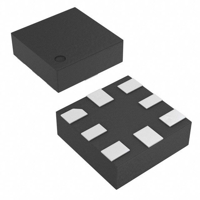
| 供应商器件封装 | 8-UQFN(1.5x1.5) |
| 其它名称 | 296-27412-1 |
| 包装 | 剪切带 (CT) |
| 商标 | Texas Instruments |
| 安装类型 | 表面贴装 |
| 安装风格 | SMD/SMT |
| 封装 | Reel |
| 封装/外壳 | 8-UFQFN |
| 封装/箱体 | UQFN-8 |
| 工作温度 | -40°C ~ 85°C |
| 工作温度范围 | - 40 C to + 85 C |
| 工厂包装数量 | 5000 |
| 最大工作温度 | + 85 C |
| 最小工作温度 | - 40 C |
| 栅极数量 | 2 Gate |
| 标准包装 | 1 |
| 特性 | 施密特触发器 |
| 电压-电源 | 0.8 V ~ 3.6 V |
| 电流-输出高,低 | 4mA,4mA |
| 电流-静态(最大值) | 0.5µA |
| 电源电压-最大 | 3.6 V |
| 电源电压-最小 | 0.8 V |
| 电路数 | 2 |
| 系列 | SN74AUP2G08 |
| 输入/输出线数量 | 2 / 2 |
| 输入数 | 2 |
| 输入线路数量 | 2 |
| 输出电压 | 3.6 V |
| 输出电流 | 20 mA |
| 输出线路数量 | 2 |
| 逻辑电平-低 | 0.7 V ~ 0.9 V |
| 逻辑电平-高 | 1.6 V ~ 2 V |
| 逻辑类型 | 与门 |
| 逻辑系列 | 74AUP |
| 高电平输出电流 | - 4 mA |


- 商务部:美国ITC正式对集成电路等产品启动337调查
- 曝三星4nm工艺存在良率问题 高通将骁龙8 Gen1或转产台积电
- 太阳诱电将投资9.5亿元在常州建新厂生产MLCC 预计2023年完工
- 英特尔发布欧洲新工厂建设计划 深化IDM 2.0 战略
- 台积电先进制程称霸业界 有大客户加持明年业绩稳了
- 达到5530亿美元!SIA预计今年全球半导体销售额将创下新高
- 英特尔拟将自动驾驶子公司Mobileye上市 估值或超500亿美元
- 三星加码芯片和SET,合并消费电子和移动部门,撤换高东真等 CEO
- 三星电子宣布重大人事变动 还合并消费电子和移动部门
- 海关总署:前11个月进口集成电路产品价值2.52万亿元 增长14.8%


PDF Datasheet 数据手册内容提取
SN74AUP2G08 www.ti.com SCES681D–JANUARY2008–REVISEDOCTOBER2010 LOW-POWER DUAL 2-INPUT POSITIVE-AND GATE CheckforSamples:SN74AUP2G08 FEATURES 1 • AvailableintheTexasInstrumentsNanoStar™ • WideOperatingV Rangeof0.8Vto3.6V CC Package • Optimizedfor3.3-VOperation • LowStatic-PowerConsumption • 3.6-VI/OToleranttoSupportMixed-Mode (ICC=0.9mAMax) SignalOperation • LowDynamic-PowerConsumption • t =5.9nsMaxat3.3V pd (C =4.3pFTypat3.3V) pd • SuitableforPoint-to-PointApplications • LowInputCapacitance(C =1.5pFTyp) i • Latch-UpPerformanceExceeds100mAPer • LowNoise–OvershootandUndershoot JESD78,ClassII <10%ofV CC • ESDPerformanceTestedPerJESD22 • I SupportsPartial-Power-DownMode off – 2000-VHuman-BodyModel Operation (A114-B,ClassII) • Schmitt-TriggerActionAllowsSlowInput – 1000-VCharged-DeviceModel(C101) TransitionandBetterSwitchingNoise ImmunityattheInput (V =250mVTypat3.3V) hys DCU PACKAGE DQE PACKAGE RSE PACKAGE YFP ORYZP PACKAGE (TOPVIEW) (TOPVIEW) (TOPVIEW) (TOPVIEW) 1A 1 8 VCC 1A 1 8 VCC VCC 1A A1 18 A2 VCC 21YB 32 76 12YB 21YB 32 76 12BY 1Y 1 8 7 1A 21YB CB11 3276 CB22 12BY GND 4 5 2A GND D1 45 D2 2A GND 4 5 2A 2B 2 6 1B 2A 3 4 5 2Y GND Seemechanicaldrawingsfordimensions. DESCRIPTION/ORDERING INFORMATION The AUP family is TI's premier solution to the industry's low-power needs in battery-powered portable applications. This family ensures a very low static- and dynamic-power consumption across the entire V range CC of 0.8 V to 3.6 V, resulting in increased battery life (see Figure 1). This product also maintains excellent signal integrity(seetheverylowundershootandovershootcharacteristicsshowninFigure2). Static-Power Consumption Dynamic-Power Consumption Switching Characteristics (m A) (pF) at 25 MHz† 100% 100% 3.5 3 80% 80% 2.5 4600%% L 3o.g3i-cV† 4600%% L LL3oVV.g3CCi-cV† oltage − V 1.512 Input Output V 0.5 20% 20% 0 0% AAUUPP 0% AUP −0.5 0 5 10 15 20 25 30 35 40 45 † Single, dual, and triple gates Time − ns † AUP1G08 data at CL = 15 pF Figure1.AUP–TheLowest-PowerFamily Figure2.ExcellentSignalIntegrity 1 Pleasebeawarethatanimportantnoticeconcerningavailability,standardwarranty,anduseincriticalapplicationsofTexas Instrumentssemiconductorproductsanddisclaimerstheretoappearsattheendofthisdatasheet. PRODUCTIONDATAinformationiscurrentasofpublicationdate. Copyright©2008–2010,TexasInstrumentsIncorporated Products conform to specifications per the terms of the Texas Instruments standard warranty. Production processing does not necessarilyincludetestingofallparameters.
SN74AUP2G08 SCES681D–JANUARY2008–REVISEDOCTOBER2010 www.ti.com Thisdual2-inputpositive-ANDgateperformstheBooleanfunctionY(cid:2)A•BorY(cid:2)A(cid:1)Binpositivelogic. NanoStar™ package technology is a major breakthrough in IC packaging concepts, using the die as the package. This device is fully specified for partial-power-down applications using I . The I circuitry disables the outputs, off off preventingdamagingcurrentbackflowthroughthedevicewhenitispowereddown. ORDERINGINFORMATION(1) T PACKAGE(2) ORDERABLEPARTNUMBER TOP-SIDEMARKING(3) A NanoStar™ –WCSP(DSBGA) Reelof3000 SN74AUP2G08YFPR ___HE_ 0.23-mmLargeBump–YFP NanoStar™ –WCSP(DSBGA) Reelof3000 SN74AUP2G08YZPR ___HE_ 0.23-mmLargeBump–YZP(Pb-free) –40°Cto85°C X2SON–DQE Reelof5000 SN74AUP2G08DQER PR QFN–RSE Reelof5000 SN74AUP2G08RSER PR VSSOP–DCU Reelof3000 SN74AUP2G08DCUR H08_ (1) Forthemostcurrentpackageandorderinginformation,seethePackageOptionAddendumattheendofthisdocument,orseetheTI websiteatwww.ti.com. (2) Packagedrawings,thermaldata,andsymbolizationareavailableatwww.ti.com/packaging. (3) YFP/YZP:Theactualtop-sidemarkinghasthreeprecedingcharacterstodenoteyear,month,andsequencecode,andonefollowing charactertodesignatethewaferfab/assemblysite.Pin1identifierindicatessolder-bumpcomposition(1=SnPb,•=Pb-free). DCU:Theactualtop-sidemarkinghasoneadditionalcharactertodenotewaferfab/assemblysite. FUNCTIONTABLE INPUTS OUTPUT A B Y L L L L H L H L L H H H LOGICDIAGRAM(POSITIVELOGIC) 1 1A 7 2 1Y 1B 5 2A 3 6 2Y 2B PinnumbersshownareforDCU,YFP,andYZPpackages. 2 SubmitDocumentationFeedback Copyright©2008–2010,TexasInstrumentsIncorporated ProductFolderLink(s):SN74AUP2G08
SN74AUP2G08 www.ti.com SCES681D–JANUARY2008–REVISEDOCTOBER2010 ABSOLUTE MAXIMUM RATINGS(1) overoperatingfree-airtemperaturerange(unlessotherwisenoted) MIN MAX UNIT V Supplyvoltagerange –0.5 4.6 V CC V Inputvoltagerange(2) –0.5 4.6 V I V Voltagerangeappliedtoanyoutputinthehigh-impedanceorpower-offstate(2) –0.5 4.6 V O V Outputvoltagerangeinthehighorlowstate(2) –0.5 V +0.5 V O CC I Inputclampcurrent V <0 –50 mA IK I I Outputclampcurrent V <0 –50 mA OK O I Continuousoutputcurrent ±20 mA O ContinuouscurrentthroughV orGND ±50 mA CC DCUpackage 227 DQEpackage 261 q Packagethermalimpedance(3) RSEpackage 253 °C/W JA YFPpackage 98.8 YZPpackage 102 T Storagetemperaturerange –65 150 °C stg (1) Stressesbeyondthoselistedunder"absolutemaximumratings"maycausepermanentdamagetothedevice.Thesearestressratings only,andfunctionaloperationofthedeviceattheseoranyotherconditionsbeyondthoseindicatedunder"recommendedoperating conditions"isnotimplied.Exposuretoabsolute-maximum-ratedconditionsforextendedperiodsmayaffectdevicereliability. (2) Theinputnegative-voltageandoutputvoltageratingsmaybeexceedediftheinputandoutputcurrentratingsareobserved. (3) ThepackagethermalimpedanceiscalculatedinaccordancewithJESD51-7. Copyright©2008–2010,TexasInstrumentsIncorporated SubmitDocumentationFeedback 3 ProductFolderLink(s):SN74AUP2G08
SN74AUP2G08 SCES681D–JANUARY2008–REVISEDOCTOBER2010 www.ti.com RECOMMENDED OPERATING CONDITIONS(1) MIN MAX UNIT V Supplyvoltage 0.8 3.6 V CC V =0.8V V CC CC V =1.1Vto1.95V 0.65×V CC CC V High-levelinputvoltage V IH V =2.3Vto2.7V 1.6 CC V =3Vto3.6V 2 CC V =0.8V 0 CC V =1.1Vto1.95V 0.35×V CC CC V Low-levelinputvoltage V IL V =2.3Vto2.7V 0.7 CC V =3Vto3.6V 0.9 CC V Inputvoltage 0 3.6 V I V Outputvoltage 0 V V O CC V =0.8V –20 mA CC V =1.1V –1.1 CC V =1.4V –1.7 CC I High-leveloutputcurrent OH V =1.65 –1.9 mA CC V =2.3V –3.1 CC V =3V –4 CC V =0.8V 20 mA CC V =1.1V 1.1 CC V =1.4V 1.7 CC I Low-leveloutputcurrent OL V =1.65V 1.9 mA CC V =2.3V 3.1 CC V =3V 4 CC Δt/Δv Inputtransitionriseorfallrate V =0.8Vto3.6V 200 ns/V CC T Operatingfree-airtemperature –40 85 °C A (1) AllunusedinputsofthedevicemustbeheldatV orGNDtoensureproperdeviceoperation.SeetheTIapplicationreport, CC ImplicationsofSloworFloatingCMOSInputs,literaturenumberSCBA004. 4 SubmitDocumentationFeedback Copyright©2008–2010,TexasInstrumentsIncorporated ProductFolderLink(s):SN74AUP2G08
SN74AUP2G08 www.ti.com SCES681D–JANUARY2008–REVISEDOCTOBER2010 ELECTRICAL CHARACTERISTICS overrecommendedoperatingfree-airtemperaturerange(unlessotherwisenoted) T =25°C T =–40°Cto85°C A A PARAMETER TESTCONDITIONS V UNIT CC MIN TYP MAX MIN MAX I =–20mA 0.8Vto3.6V V –0.1 V –0.1 OH CC CC I =–1.1mA 1.1V 0.75×V 0.7×V OH CC CC I =–1.7mA 1.4V 1.11 1.03 OH I =–1.9mA 1.65V 1.32 1.3 OH V V OH I =–2.3mA 2.05 1.97 OH 2.3V I =–3.1mA 1.9 1.85 OH I =–2.7mA 2.72 2.67 OH 3V I =–4mA 2.6 2.55 OH I =20mA 0.8Vto3.6V 0.1 0.1 OL I =1.1mA 1.1V 0.3×V 0.3×V OL CC CC I =1.7mA 1.4V 0.31 0.37 OL I =1.9mA 1.65V 0.31 0.35 OL V V OL I =2.3mA 0.31 0.33 OL 2.3V I =3.1mA 0.44 0.45 OL I =2.7mA 0.31 0.33 OL 3V I =4mA 0.44 0.45 OL I AorBinput V =GNDto3.6V 0Vto3.6V 0.1 0.5 mA I I I V orV =0Vto3.6V 0V 0.2 0.6 mA off I O ΔI V orV =0Vto3.6V 0Vto0.2V 0.2 0.9 mA off I O V =GNDorI =0 I I O 0.8Vto3.6V 0.5 0.9 mA CC (V to3.6V) CC ΔI V =V –0.6V(1),I =0 3.3V 40 50 mA CC I CC O 0V 2 C V =V orGND pF i I CC 3.6V 2 C V =GND 0V 3 pF o O (1) OneinputatV –0.6V,otherinputatV orGND CC CC Copyright©2008–2010,TexasInstrumentsIncorporated SubmitDocumentationFeedback 5 ProductFolderLink(s):SN74AUP2G08
SN74AUP2G08 SCES681D–JANUARY2008–REVISEDOCTOBER2010 www.ti.com SWITCHING CHARACTERISTICS overrecommendedoperatingfree-airtemperaturerange,C =5pF(unlessotherwisenoted)(seeFigure3andFigure4) L FROM TO TA=25°C TA=–40°Cto85°C PARAMETER V UNIT (INPUT) (OUTPUT) CC MIN TYP MAX MIN MAX 0.8V 19.8 1.2V±0.1V 0.5 7.8 18.8 0.5 19.8 1.5V±0.1V 0.5 5.4 11.8 0.5 13.9 t AorB Y ns pd 1.8V±0.15V 0.5 4.3 9 0.5 11.1 2.5V±0.2V 0.5 3 5.7 0.5 7.8 3.3V±0.3V 0.5 2.4 4.6 0.5 5.9 SWITCHING CHARACTERISTICS overrecommendedoperatingfree-airtemperaturerange,C =10pF(unlessotherwisenoted)(seeFigure3andFigure4) L FROM TO TA=25°C TA=–40°Cto85°C PARAMETER V UNIT (INPUT) (OUTPUT) CC MIN TYP MAX MIN MAX 0.8V 23.1 1.2V±0.1V 0.5 8.9 21.1 0.5 22 1.5V±0.1V 0.8 6.3 13.2 0.5 15.1 t AorB Y ns pd 1.8V±0.15V 0.6 5 10.1 0.5 12.2 2.5V±0.2V 0.5 3.6 7.4 0.5 9 3.3V±0.3V 0.5 2.9 5.1 0.5 6.5 6 SubmitDocumentationFeedback Copyright©2008–2010,TexasInstrumentsIncorporated ProductFolderLink(s):SN74AUP2G08
SN74AUP2G08 www.ti.com SCES681D–JANUARY2008–REVISEDOCTOBER2010 SWITCHING CHARACTERISTICS overrecommendedoperatingfree-airtemperaturerange,C =15pF(unlessotherwisenoted)(seeFigure3andFigure4) L FROM TO TA=25°C TA=–40°Cto85°C PARAMETER V UNIT (INPUT) (OUTPUT) CC MIN TYP MAX MIN MAX 0.8V 24.7 1.2V±0.1V 0.5 9.8 21.7 0.5 22.7 1.5V±0.1V 1.3 4.6 14 0.5 15.7 t AorB Y ns pd 1.8V±0.15V 1.2 5.5 10.6 0.5 12.6 2.5V±0.2V 0.7 4 7 0.5 8.9 3.3V±0.3V 0.9 3.3 5.5 0.5 6.9 SWITCHING CHARACTERISTICS overrecommendedoperatingfree-airtemperaturerange,C =30pF(unlessotherwisenoted)(seeFigure3andFigure4) L FROM TO TA=25°C TA=–40°Cto85°C PARAMETER V UNIT (INPUT) (OUTPUT) CC MIN TYP MAX MIN MAX 0.8V 31.8 1.2V±0.1V 0.6 12.6 26.3 0.5 27 1.5V±0.1V 2.5 9 16.6 0.7 18.3 t AorB Y ns pd 1.8V±0.15V 2.3 7.3 12.9 0.5 14.8 2.5V±0.2V 2.1 5.4 8.8 0.8 10.5 3.3V±0.3V 2.1 4.5 6.7 0.9 8.2 OPERATING CHARACTERISTICS T =25°C A PARAMETER TESTCONDITIONS V TYP UNIT CC 0.8V 4 1.2V±0.1V 4 1.5V±0.1V 4 C Powerdissipationcapacitance f=10MHz pF pd 1.8V±0.15V 4 2.5V±0.2V 4.1 3.3V±0.3V 4.3 Copyright©2008–2010,TexasInstrumentsIncorporated SubmitDocumentationFeedback 7 ProductFolderLink(s):SN74AUP2G08
SN74AUP2G08 SCES681D–JANUARY2008–REVISEDOCTOBER2010 www.ti.com PARAMETER MEASUREMENT INFORMATION (Propagation Delays, Setup and Hold Times, and Pulse Duration) From Output Under Test CL 1 MW (see Note A) LOAD CIRCUIT VCC = 0.8 V VC±C 0=. 11 .V2 V VC±C 0=. 11 .V5 V VC±C 0 =.1 15. 8V V VC±C 0=. 22 .V5 V VC±C 0=. 33 .V3 V CL 5, 10, 15, 30 pF 5, 10, 15, 30 pF 5, 10, 15, 30 pF 5, 10, 15, 30 pF 5, 10, 15, 30 pF 5, 10, 15, 30 pF VM VCC/2 VCC/2 VCC/2 VCC/2 VCC/2 VCC/2 VI VCC VCC VCC VCC VCC VCC tw VCC Input VCC/2 VCC/2 VI 0 V Input VM VM 0 V VOLTAGE WAVEFORMS PULSE DURATION tPLH tPHL Output VM VM VOH VCC VOL Timing Input VCC/2 0 V tPHL tPLH VOH tsu th Output VM VM VCC VOL Data Input VCC/2 VCC/2 0 V VOLTAGE WAVEFORMS PROPAGATION DELAY TIMES VOLTAGE WAVEFORMS INVERTING AND NONINVERTING OUTPUTS SETUP AND HOLD TIMES NOTES: A. CL includes probe and jig capacitance. B. All input pulses are supplied by generators having the following characteristics: PRR ≤ 10 MHz, ZO = 50 W , slew rate ≥ 1 V/ns. C. The outputs are measured one at a time, with one transition per measurement. D. tPLH and tPHL are the same as tpd. E. All parameters and waveforms are not applicable to all devices. Figure3. LoadCircuitandVoltageWaveforms 8 SubmitDocumentationFeedback Copyright©2008–2010,TexasInstrumentsIncorporated ProductFolderLink(s):SN74AUP2G08
SN74AUP2G08 www.ti.com SCES681D–JANUARY2008–REVISEDOCTOBER2010 PARAMETER MEASUREMENT INFORMATION (Enable and Disable Times) 2 × VCC 5 kW S1 From Output Under Test GND TEST S1 CL 5 kW tPLZ/tPZL 2 × VCC (see Note A) tPHZ/tPZH GND LOAD CIRCUIT VCC = 0.8 V VC±C 0=. 11 .V2 V VC±C 0=. 11 .V5 V VC±C 0 =.1 15. 8V V VC±C 0=. 22 .V5 V VC±C 0=. 33 .V3 V CL 5, 10, 15, 30 pF 5, 10, 15, 30 pF 5, 10, 15, 30 pF 5, 10, 15, 30 pF 5, 10, 15, 30 pF 5, 10, 15, 30 pF VM VCC/2 VCC/2 VCC/2 VCC/2 VCC/2 VCC/2 VI VCC VCC VCC VCC VCC VCC VD 0.1 V 0.1 V 0.1 V 0.15 V 0.15 V 0.3 V VCC Output Control VCC/2 VCC/2 0 V tPZL tPLZ Output Waveform 1 VCC S1 at 2 × VCC VCC/2 VOL + VD (see Note B) VOL tPZH tPHZ Output WSa1v eafto GrmN D2 VCC/2 VOH - VD VOH ≈0 V (see Note B) VOLTAGE WAVEFORMS ENABLE AND DISABLE TIMES LOW- AND HIGH-LEVEL ENABLING NOTES: A. CL includes probe and jig capacitance. B. Waveform 1 is for an output with internal conditions such that the output is low, except when disabled by the output control. Waveform2 is for an output with internal conditions such that the output is high, except when disabled by the output control. C. All input pulses are supplied by generators having the following characteristics: PRR ≤ 10 MHz, ZO = 50 W , slew rate ≥ 1 V/ns. D. The outputs are measured one at a time, with one transition per measurement. E. tPLZ and tPHZ are the same as tdis. F. tPZL and tPZH are the same as ten. G. All parameters and waveforms are not applicable to all devices. Figure4. LoadCircuitandVoltageWaveforms Copyright©2008–2010,TexasInstrumentsIncorporated SubmitDocumentationFeedback 9 ProductFolderLink(s):SN74AUP2G08
PACKAGE OPTION ADDENDUM www.ti.com 24-Mar-2017 PACKAGING INFORMATION Orderable Device Status Package Type Package Pins Package Eco Plan Lead/Ball Finish MSL Peak Temp Op Temp (°C) Device Marking Samples (1) Drawing Qty (2) (6) (3) (4/5) SN74AUP2G08DCUR ACTIVE VSSOP DCU 8 3000 Green (RoHS CU NIPDAU Level-1-260C-UNLIM -40 to 85 H08R & no Sb/Br) SN74AUP2G08DQER ACTIVE X2SON DQE 8 5000 Green (RoHS CU NIPDAUAG Level-1-260C-UNLIM -40 to 85 PR & no Sb/Br) SN74AUP2G08RSER ACTIVE UQFN RSE 8 5000 Green (RoHS CU NIPDAUAG Level-1-260C-UNLIM -40 to 85 PR & no Sb/Br) SN74AUP2G08YFPR ACTIVE DSBGA YFP 8 3000 Green (RoHS SNAGCU Level-1-260C-UNLIM -40 to 85 HEN & no Sb/Br) SN74AUP2G08YZPR ACTIVE DSBGA YZP 8 3000 Green (RoHS SNAGCU Level-1-260C-UNLIM -40 to 85 HEN & no Sb/Br) (1) The marketing status values are defined as follows: ACTIVE: Product device recommended for new designs. LIFEBUY: TI has announced that the device will be discontinued, and a lifetime-buy period is in effect. NRND: Not recommended for new designs. Device is in production to support existing customers, but TI does not recommend using this part in a new design. PREVIEW: Device has been announced but is not in production. Samples may or may not be available. OBSOLETE: TI has discontinued the production of the device. (2) Eco Plan - The planned eco-friendly classification: Pb-Free (RoHS), Pb-Free (RoHS Exempt), or Green (RoHS & no Sb/Br) - please check http://www.ti.com/productcontent for the latest availability information and additional product content details. TBD: The Pb-Free/Green conversion plan has not been defined. Pb-Free (RoHS): TI's terms "Lead-Free" or "Pb-Free" mean semiconductor products that are compatible with the current RoHS requirements for all 6 substances, including the requirement that lead not exceed 0.1% by weight in homogeneous materials. Where designed to be soldered at high temperatures, TI Pb-Free products are suitable for use in specified lead-free processes. Pb-Free (RoHS Exempt): This component has a RoHS exemption for either 1) lead-based flip-chip solder bumps used between the die and package, or 2) lead-based die adhesive used between the die and leadframe. The component is otherwise considered Pb-Free (RoHS compatible) as defined above. Green (RoHS & no Sb/Br): TI defines "Green" to mean Pb-Free (RoHS compatible), and free of Bromine (Br) and Antimony (Sb) based flame retardants (Br or Sb do not exceed 0.1% by weight in homogeneous material) (3) MSL, Peak Temp. - The Moisture Sensitivity Level rating according to the JEDEC industry standard classifications, and peak solder temperature. (4) There may be additional marking, which relates to the logo, the lot trace code information, or the environmental category on the device. (5) Multiple Device Markings will be inside parentheses. Only one Device Marking contained in parentheses and separated by a "~" will appear on a device. If a line is indented then it is a continuation of the previous line and the two combined represent the entire Device Marking for that device. Addendum-Page 1
PACKAGE OPTION ADDENDUM www.ti.com 24-Mar-2017 (6) Lead/Ball Finish - Orderable Devices may have multiple material finish options. Finish options are separated by a vertical ruled line. Lead/Ball Finish values may wrap to two lines if the finish value exceeds the maximum column width. Important Information and Disclaimer:The information provided on this page represents TI's knowledge and belief as of the date that it is provided. TI bases its knowledge and belief on information provided by third parties, and makes no representation or warranty as to the accuracy of such information. Efforts are underway to better integrate information from third parties. TI has taken and continues to take reasonable steps to provide representative and accurate information but may not have conducted destructive testing or chemical analysis on incoming materials and chemicals. TI and TI suppliers consider certain information to be proprietary, and thus CAS numbers and other limited information may not be available for release. In no event shall TI's liability arising out of such information exceed the total purchase price of the TI part(s) at issue in this document sold by TI to Customer on an annual basis. Addendum-Page 2
PACKAGE MATERIALS INFORMATION www.ti.com 3-Aug-2017 TAPE AND REEL INFORMATION *Alldimensionsarenominal Device Package Package Pins SPQ Reel Reel A0 B0 K0 P1 W Pin1 Type Drawing Diameter Width (mm) (mm) (mm) (mm) (mm) Quadrant (mm) W1(mm) SN74AUP2G08DCUR VSSOP DCU 8 3000 180.0 8.4 2.25 3.35 1.05 4.0 8.0 Q3 SN74AUP2G08DQER X2SON DQE 8 5000 180.0 8.4 1.2 1.6 0.55 4.0 8.0 Q1 SN74AUP2G08RSER UQFN RSE 8 5000 180.0 8.4 1.7 1.7 0.7 4.0 8.0 Q2 SN74AUP2G08YFPR DSBGA YFP 8 3000 178.0 9.2 0.9 1.75 0.6 4.0 8.0 Q1 SN74AUP2G08YZPR DSBGA YZP 8 3000 178.0 9.2 1.02 2.02 0.63 4.0 8.0 Q1 PackMaterials-Page1
PACKAGE MATERIALS INFORMATION www.ti.com 3-Aug-2017 *Alldimensionsarenominal Device PackageType PackageDrawing Pins SPQ Length(mm) Width(mm) Height(mm) SN74AUP2G08DCUR VSSOP DCU 8 3000 202.0 201.0 28.0 SN74AUP2G08DQER X2SON DQE 8 5000 202.0 201.0 28.0 SN74AUP2G08RSER UQFN RSE 8 5000 202.0 201.0 28.0 SN74AUP2G08YFPR DSBGA YFP 8 3000 220.0 220.0 35.0 SN74AUP2G08YZPR DSBGA YZP 8 3000 220.0 220.0 35.0 PackMaterials-Page2
None
None
None
None
PACKAGE OUTLINE RSE0008A UQFN - 0.6 mm max height SCALE 7.000 PLASTIC QUAD FLATPACK - NO LEAD 1.55 B 1.45 A PIN 1 INDEX AREA 1.55 1.45 0.6 C 0.5 SEATING PLANE 0.05 0.00 0.05 C 0.35 2X 0.25 0.4 6X 0.3 0.1 C A B (0.12) 0.05 C 2X 0.45 TYP 0.35 4 3 5 2X SYMM 1 0.25 2X 0.15 7 1 0.1 C A B 4X 0.5 0.05 C 8 0.3 SYMM 4X 0.2 0.1 C A B PIN 1 ID 0.05 C (45 X 0.1) 4220323/B 03/2018 NOTES: 1. All linear dimensions are in millimeters. Any dimensions in parenthesis are for reference only. Dimensioning and tolerancing per ASME Y14.5M. 2. This drawing is subject to change without notice. www.ti.com
EXAMPLE BOARD LAYOUT RSE0008A UQFN - 0.6 mm max height PLASTIC QUAD FLATPACK - NO LEAD SYMM (R0.05) TYP 2X (0.6) 8 6X (0.55) 1 7 4X (0.25) SYMM (1.3) 2X 4X (0.5) (0.2) 5 3 4 2X (0.3) (1.35) LAND PATTERN EXAMPLE SCALE:30X 0.07 MAX 0.07 MIN ALL AROUND ALL AROUND SOLDER MASK METAL OPENING SOLDER MASK METAL OPENING UNDER SOLDER MASK NON SOLDER MASK SOLDER MASK DEFINED DEFINED (PREFERRED) SOLDER MASK DETAILS NOT TO SCALE 4220323/B 03/2018 NOTES: (continued) 3. For more information, see Texas Instruments literature number SLUA271 (www.ti.com/lit/slua271). www.ti.com
EXAMPLE STENCIL DESIGN RSE0008A UQFN - 0.6 mm max height PLASTIC QUAD FLATPACK - NO LEAD SYMM (R0.05) TYP 2X (0.6) 8 6X (0.55) 1 7 4X (0.25) SYMM (1.3) 4X (0.5) 2X (0.2) 5 3 4 2X (0.3) (1.35) SOLDER PASTE EXAMPLE BASED ON 0.1 mm THICKNESS SCALE: 30X 4220323/B 03/2018 NOTES: (continued) 5. Laser cutting apertures with trapezoidal walls and rounded corners may offer better paste release. IPC-7525 may have alternate design recommendations. www.ti.com
PACKAGE OUTLINE YZP0008 DSBGA - 0.5 mm max height SCALE 8.000 DIE SIZE BALL GRID ARRAY B E A BALL A1 CORNER D C 0.5 MAX SEATING PLANE 0.19 0.05 C 0.15 BALL TYP 0.5 TYP D C SYMM 1.5 D: Max = 1.918 mm, Min =1 .858 mm TYP B E: Max = 0.918 mm, Min =0 .858 mm 0.5 TYP A 0.25 8X 1 2 0.21 0.015 C A B SYMM 4223082/A 07/2016 NOTES: 1. All linear dimensions are in millimeters. Any dimensions in parenthesis are for reference only. Dimensioning and tolerancing per ASME Y14.5M. 2. This drawing is subject to change without notice. www.ti.com
EXAMPLE BOARD LAYOUT YZP0008 DSBGA - 0.5 mm max height DIE SIZE BALL GRID ARRAY (0.5) TYP 8X ( 0.23) 1 2 A (0.5) TYP B SYMM C D SYMM LAND PATTERN EXAMPLE SCALE:40X SOLDER MASK 0.05 MAX 0.05 MIN ( 0.23) OPENING SOLDER MASK OPENING ( 0.23) METAL METAL UNDER SOLDER MASK NON-SOLDER MASK SOLDER MASK DEFINED DEFINED (PREFERRED) SOLDER MASK DETAILS NOT TO SCALE 4223082/A 07/2016 NOTES: (continued) 3. Final dimensions may vary due to manufacturing tolerance considerations and also routing constraints. For more information, see Texas Instruments literature number SNVA009 (www.ti.com/lit/snva009). www.ti.com
EXAMPLE STENCIL DESIGN YZP0008 DSBGA - 0.5 mm max height DIE SIZE BALL GRID ARRAY (0.5) TYP 8X ( 0.25) (R0.05) TYP 1 2 A (0.5) TYP B SYMM C METAL TYP D SYMM SOLDER PASTE EXAMPLE BASED ON 0.1 mm THICK STENCIL SCALE:40X 4223082/A 07/2016 NOTES: (continued) 4. Laser cutting apertures with trapezoidal walls and rounded corners may offer better paste release. www.ti.com
D: Max = 1.59 mm, Min = 1.53 mm E: Max = 0.79 mm, Min = 0.73 mm
IMPORTANTNOTICE TexasInstrumentsIncorporated(TI)reservestherighttomakecorrections,enhancements,improvementsandotherchangestoits semiconductorproductsandservicesperJESD46,latestissue,andtodiscontinueanyproductorserviceperJESD48,latestissue.Buyers shouldobtainthelatestrelevantinformationbeforeplacingordersandshouldverifythatsuchinformationiscurrentandcomplete. TI’spublishedtermsofsaleforsemiconductorproducts(http://www.ti.com/sc/docs/stdterms.htm)applytothesaleofpackagedintegrated circuitproductsthatTIhasqualifiedandreleasedtomarket.AdditionaltermsmayapplytotheuseorsaleofothertypesofTIproductsand services. ReproductionofsignificantportionsofTIinformationinTIdatasheetsispermissibleonlyifreproductioniswithoutalterationandis accompaniedbyallassociatedwarranties,conditions,limitations,andnotices.TIisnotresponsibleorliableforsuchreproduced documentation.Informationofthirdpartiesmaybesubjecttoadditionalrestrictions.ResaleofTIproductsorserviceswithstatements differentfromorbeyondtheparametersstatedbyTIforthatproductorservicevoidsallexpressandanyimpliedwarrantiesforthe associatedTIproductorserviceandisanunfairanddeceptivebusinesspractice.TIisnotresponsibleorliableforanysuchstatements. BuyersandotherswhoaredevelopingsystemsthatincorporateTIproducts(collectively,“Designers”)understandandagreethatDesigners remainresponsibleforusingtheirindependentanalysis,evaluationandjudgmentindesigningtheirapplicationsandthatDesignershave fullandexclusiveresponsibilitytoassurethesafetyofDesigners'applicationsandcomplianceoftheirapplications(andofallTIproducts usedinorforDesigners’applications)withallapplicableregulations,lawsandotherapplicablerequirements.Designerrepresentsthat,with respecttotheirapplications,Designerhasallthenecessaryexpertisetocreateandimplementsafeguardsthat(1)anticipatedangerous consequencesoffailures,(2)monitorfailuresandtheirconsequences,and(3)lessenthelikelihoodoffailuresthatmightcauseharmand takeappropriateactions.DesigneragreesthatpriortousingordistributinganyapplicationsthatincludeTIproducts,Designerwill thoroughlytestsuchapplicationsandthefunctionalityofsuchTIproductsasusedinsuchapplications. TI’sprovisionoftechnical,applicationorotherdesignadvice,qualitycharacterization,reliabilitydataorotherservicesorinformation, including,butnotlimitedto,referencedesignsandmaterialsrelatingtoevaluationmodules,(collectively,“TIResources”)areintendedto assistdesignerswhoaredevelopingapplicationsthatincorporateTIproducts;bydownloading,accessingorusingTIResourcesinany way,Designer(individuallyor,ifDesignerisactingonbehalfofacompany,Designer’scompany)agreestouseanyparticularTIResource solelyforthispurposeandsubjecttothetermsofthisNotice. TI’sprovisionofTIResourcesdoesnotexpandorotherwisealterTI’sapplicablepublishedwarrantiesorwarrantydisclaimersforTI products,andnoadditionalobligationsorliabilitiesarisefromTIprovidingsuchTIResources.TIreservestherighttomakecorrections, enhancements,improvementsandotherchangestoitsTIResources.TIhasnotconductedanytestingotherthanthatspecifically describedinthepublisheddocumentationforaparticularTIResource. Designerisauthorizedtouse,copyandmodifyanyindividualTIResourceonlyinconnectionwiththedevelopmentofapplicationsthat includetheTIproduct(s)identifiedinsuchTIResource.NOOTHERLICENSE,EXPRESSORIMPLIED,BYESTOPPELOROTHERWISE TOANYOTHERTIINTELLECTUALPROPERTYRIGHT,ANDNOLICENSETOANYTECHNOLOGYORINTELLECTUALPROPERTY RIGHTOFTIORANYTHIRDPARTYISGRANTEDHEREIN,includingbutnotlimitedtoanypatentright,copyright,maskworkright,or otherintellectualpropertyrightrelatingtoanycombination,machine,orprocessinwhichTIproductsorservicesareused.Information regardingorreferencingthird-partyproductsorservicesdoesnotconstitutealicensetousesuchproductsorservices,orawarrantyor endorsementthereof.UseofTIResourcesmayrequirealicensefromathirdpartyunderthepatentsorotherintellectualpropertyofthe thirdparty,oralicensefromTIunderthepatentsorotherintellectualpropertyofTI. TIRESOURCESAREPROVIDED“ASIS”ANDWITHALLFAULTS.TIDISCLAIMSALLOTHERWARRANTIESOR REPRESENTATIONS,EXPRESSORIMPLIED,REGARDINGRESOURCESORUSETHEREOF,INCLUDINGBUTNOTLIMITEDTO ACCURACYORCOMPLETENESS,TITLE,ANYEPIDEMICFAILUREWARRANTYANDANYIMPLIEDWARRANTIESOF MERCHANTABILITY,FITNESSFORAPARTICULARPURPOSE,ANDNON-INFRINGEMENTOFANYTHIRDPARTYINTELLECTUAL PROPERTYRIGHTS.TISHALLNOTBELIABLEFORANDSHALLNOTDEFENDORINDEMNIFYDESIGNERAGAINSTANYCLAIM, INCLUDINGBUTNOTLIMITEDTOANYINFRINGEMENTCLAIMTHATRELATESTOORISBASEDONANYCOMBINATIONOF PRODUCTSEVENIFDESCRIBEDINTIRESOURCESOROTHERWISE.INNOEVENTSHALLTIBELIABLEFORANYACTUAL, DIRECT,SPECIAL,COLLATERAL,INDIRECT,PUNITIVE,INCIDENTAL,CONSEQUENTIALOREXEMPLARYDAMAGESIN CONNECTIONWITHORARISINGOUTOFTIRESOURCESORUSETHEREOF,ANDREGARDLESSOFWHETHERTIHASBEEN ADVISEDOFTHEPOSSIBILITYOFSUCHDAMAGES. UnlessTIhasexplicitlydesignatedanindividualproductasmeetingtherequirementsofaparticularindustrystandard(e.g.,ISO/TS16949 andISO26262),TIisnotresponsibleforanyfailuretomeetsuchindustrystandardrequirements. WhereTIspecificallypromotesproductsasfacilitatingfunctionalsafetyorascompliantwithindustryfunctionalsafetystandards,such productsareintendedtohelpenablecustomerstodesignandcreatetheirownapplicationsthatmeetapplicablefunctionalsafetystandards andrequirements.Usingproductsinanapplicationdoesnotbyitselfestablishanysafetyfeaturesintheapplication.Designersmust ensurecompliancewithsafety-relatedrequirementsandstandardsapplicabletotheirapplications.DesignermaynotuseanyTIproductsin life-criticalmedicalequipmentunlessauthorizedofficersofthepartieshaveexecutedaspecialcontractspecificallygoverningsuchuse. Life-criticalmedicalequipmentismedicalequipmentwherefailureofsuchequipmentwouldcauseseriousbodilyinjuryordeath(e.g.,life support,pacemakers,defibrillators,heartpumps,neurostimulators,andimplantables).Suchequipmentincludes,withoutlimitation,all medicaldevicesidentifiedbytheU.S.FoodandDrugAdministrationasClassIIIdevicesandequivalentclassificationsoutsidetheU.S. TImayexpresslydesignatecertainproductsascompletingaparticularqualification(e.g.,Q100,MilitaryGrade,orEnhancedProduct). Designersagreethatithasthenecessaryexpertisetoselecttheproductwiththeappropriatequalificationdesignationfortheirapplications andthatproperproductselectionisatDesigners’ownrisk.Designersaresolelyresponsibleforcompliancewithalllegalandregulatory requirementsinconnectionwithsuchselection. DesignerwillfullyindemnifyTIanditsrepresentativesagainstanydamages,costs,losses,and/orliabilitiesarisingoutofDesigner’snon- compliancewiththetermsandprovisionsofthisNotice. MailingAddress:TexasInstruments,PostOfficeBox655303,Dallas,Texas75265 Copyright©2018,TexasInstrumentsIncorporated