ICGOO在线商城 > 集成电路(IC) > 逻辑 - 栅极和逆变器 > SN74AUP1G08DCKT
 Datasheet下载
- 型号: SN74AUP1G08DCKT
- 制造商: Texas Instruments
- 库位|库存: xxxx|xxxx
- 要求:
| 数量阶梯 | 香港交货 | 国内含税 |
| +xxxx | $xxxx | ¥xxxx |
查看当月历史价格
查看今年历史价格
SN74AUP1G08DCKT产品简介:
ICGOO电子元器件商城为您提供SN74AUP1G08DCKT由Texas Instruments设计生产,在icgoo商城现货销售,并且可以通过原厂、代理商等渠道进行代购。 SN74AUP1G08DCKT价格参考¥12.17-¥12.17。Texas InstrumentsSN74AUP1G08DCKT封装/规格:逻辑 - 栅极和逆变器, AND Gate IC 1 Channel SC-70-5。您可以下载SN74AUP1G08DCKT参考资料、Datasheet数据手册功能说明书,资料中有SN74AUP1G08DCKT 详细功能的应用电路图电压和使用方法及教程。
SN74AUP1G08DCKT 是由 Texas Instruments(德州仪器)生产的一款单通道 CMOS 与门(AND Gate)逻辑器件,属于“逻辑 - 栅极和逆变器”类别。其主要应用场景如下:

 1. 数字信号处理
   - 该器件可用于数字电路中实现基本的逻辑运算功能,例如信号的“与”操作。在复杂的数字系统中,它可作为构建模块,用于组合逻辑电路的设计。
   - 适用于数据路径控制、地址解码、时钟信号生成等场景。

 2. 嵌入式系统
   - 在微控制器或 FPGA 系统中,SN74AUP1G08DCKT 可用于信号同步、使能控制或条件检测。
   - 例如,在外设接口设计中,可以用来控制数据传输的使能信号。

 3. 电源管理
   - 在低功耗应用中,该器件的超低电压工作能力(支持 0.8V 至 3.6V)使其适合用作电源管理电路中的逻辑控制单元。
   - 可用于电池供电设备(如手持设备、传感器节点)中的信号控制。

 4. 通信接口
   - 在串行通信协议(如 I2C、SPI 或 UART)中,可以用作信号使能或数据选择的逻辑控制。
   - 例如,在多路复用器设计中,它可以与其他逻辑器件配合使用,实现信号的选择与切换。

 5. 消费电子
   - 应用于音频、视频设备中的信号处理部分,例如音视频切换、模式选择等功能。
   - 在家用电器(如智能电视、音响系统)中,可用作简单的逻辑控制单元。

 6. 工业自动化
   - 在工业控制系统中,可用于传感器信号处理、状态监测或逻辑判断。
   - 例如,在 PLC(可编程逻辑控制器)或分布式控制系统中,作为信号处理的基本组件。

 7. 汽车电子
   - 由于其低功耗特性和宽电压范围,SN74AUP1G08DCKT 可用于汽车电子系统中的信号控制,例如车内照明控制、传感器信号处理等。

 特性优势:
- 低功耗:适合对功耗要求严格的便携式设备。
- 宽电压范围:兼容多种供电环境,增强了设计灵活性。
- 小型封装(X2SON 封装):节省 PCB 空间,适合高密度设计。

综上所述,SN74AUP1G08DCKT 主要应用于需要低功耗、小型化和高效逻辑控制的场景,广泛覆盖消费电子、工业控制、通信和汽车电子等领域。
| 参数 | 数值 |
| 产品目录 | 集成电路 (IC)半导体 |
| 描述 | IC GATE AND 1CH 2-INP SC-70-5逻辑门 Lo PWR SNGL 2Input Pos AND Gate |
| 产品分类 | |
| 品牌 | Texas Instruments |
| 产品手册 | http://www.ti.com/lit/gpn/sn74aup1g08 |
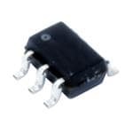
| 产品图片 |
|
| rohs | 符合RoHS无铅 / 符合限制有害物质指令(RoHS)规范要求 |
| 产品系列 | 逻辑集成电路,逻辑门,Texas Instruments SN74AUP1G08DCKT74AUP |
| 数据手册 | |
| 产品型号 | SN74AUP1G08DCKT |
| PCN设计/规格 | |
| 不同V、最大CL时的最大传播延迟 | 6.2ns @ 3.3V, 30pF |
| 产品 | AND |
| 产品种类 | 逻辑门 |
| 传播延迟时间 | 20.9 ns |
| 低电平输出电流 | 4 mA |
| 供应商器件封装 | SC-70-5 |
| 其它名称 | 296-32258-2 |
| 包装 | 带卷 (TR) |
| 单位重量 | 2.500 mg |
| 商标 | Texas Instruments |
| 安装类型 | 表面贴装 |
| 安装风格 | SMD/SMT |
| 封装 | Reel |
| 封装/外壳 | 6-TSSOP(5 引线),SC-88A,SOT-353 |
| 封装/箱体 | SC-70-5 |
| 工作温度 | -40°C ~ 85°C |
| 工厂包装数量 | 250 |
| 最大工作温度 | + 85 C |
| 最小工作温度 | - 40 C |
| 栅极数量 | 1 Gate |
| 标准包装 | 250 |
| 特性 | 施密特触发器 |
| 电压-电源 | 0.8 V ~ 3.6 V |
| 电流-输出高,低 | 4mA,4mA |
| 电流-静态(最大值) | 0.5µA |
| 电源电压-最大 | 3.6 V |
| 电源电压-最小 | 0.8 V |
| 电路数 | 1 |
| 系列 | SN74AUP1G08 |
| 输入/输出线数量 | 2 / 1 |
| 输入数 | 2 |
| 输入线路数量 | 2 |
| 输出线路数量 | 1 |
| 逻辑电平-低 | 0.7 V ~ 0.9 V |
| 逻辑电平-高 | 1.6 V ~ 2 V |
| 逻辑类型 | 与门 |
| 逻辑系列 | 74AUP |
| 高电平输出电流 | - 4 mA |


- 商务部:美国ITC正式对集成电路等产品启动337调查
- 曝三星4nm工艺存在良率问题 高通将骁龙8 Gen1或转产台积电
- 太阳诱电将投资9.5亿元在常州建新厂生产MLCC 预计2023年完工
- 英特尔发布欧洲新工厂建设计划 深化IDM 2.0 战略
- 台积电先进制程称霸业界 有大客户加持明年业绩稳了
- 达到5530亿美元!SIA预计今年全球半导体销售额将创下新高
- 英特尔拟将自动驾驶子公司Mobileye上市 估值或超500亿美元
- 三星加码芯片和SET,合并消费电子和移动部门,撤换高东真等 CEO
- 三星电子宣布重大人事变动 还合并消费电子和移动部门
- 海关总署:前11个月进口集成电路产品价值2.52万亿元 增长14.8%


PDF Datasheet 数据手册内容提取
Product Sample & Technical Tools & Support & Folder Buy Documents Software Community SN74AUP1G08 SCES502P–NOVEMBER2003–REVISEDJUNE2016 SN74AUP1G08 Low-Power Single 2-Input Positive-AND Gate 1 Features 2 Applications • AvailableintheUltraSmall0.64mm2Package • ATCASolutions 1 (DPW)With0.5-mmPitch • ActiveNoiseCancellation(ANC) • LowStatic-PowerConsumption: • BarcodeScanner I =0.9μAMaximum CC • BloodPressureMonitor • LowDynamic-PowerConsumption: • CPAPMachine C =4.3pFTypicalat3.3V pd • CableSolutions • LowInputCapacitance:C =1.5pFTypical i • DLP3DMachineVision,HyperspectralImaging, • LowNoise:OvershootandUndershoot OpticalNetworking,andSpectroscopy <10%ofV CC • E-Book • I SupportsLiveInsertion,Partial-Power-Down off • EmbeddedPC Mode,andBackDriveProtection • FieldTransmitter:TemperatureorPressure • Schmitt-TriggerActionAllowsSlowInput Sensor TransitionandBetterSwitchingNoiseImmunityat • FingerprintBiometrics theInput(V =250mVTypicalat3.3V) hys • HVAC:Heating,Ventilating,andAirConditioning • WideOperatingV Rangeof0.8Vto3.6V CC • Network-AttachedStorage(NAS) • Optimizedfor3.3-VOperation • ServerMotherboardandPSU • 3.6-VI/OToleranttoSupportMixed-ModeSignal Operation • SoftwareDefinedRadio(SDR) • t =4.3nsMaximumat3.3V • TV:High-Definition(HDTV),LCD,andDigital pd • SuitableforPoint-to-PointApplications • VideoCommunicationsSystem • Latch-UpPerformanceExceeds100mAPer • WirelessDataAccessCard,Headset,Keyboard, JESD78,ClassII Mouse,andLANCard • ESDPerformanceTestedPerJESD22 • X-ray:BaggageScanner,Medical,andDental – 2000-VHuman-BodyModel 3 Description (A114-B,ClassII) This single 2-input positive-AND gate is designed for – 1000-VCharged-DeviceModel(C101) 0.8-V to 3.6-V V operation and performs the CC SimplifiedSchematic Boolean function Y=A·Bor Y= A+B in positive logic. A Y B DeviceInformation(1) PARTNUMBER PACKAGE BODYSIZE(NOM) SN74AUP1G08DBV SOT-23(5) 2.90mm×1.60mm SN74AUP1G08DRL SOT(5) 1.60mm×1.20mm SN74AUP1G08DRY SON(6) 1.45mm×1.00mm SN74AUP1G08DPW X2SON(5) 0.80mm×0.80mm SN74AUP1G08YZP DSBGA(5) 1.37mm×0.88mm SN74AUP1G08DCK SC70(5) 1.25mmx2.00mm SN74AUP1G08DSF SON(6) 1.00mmx1.00mm SN74AUP1G08YFP DSBGA(6) 1.16mmx0.76mm (1) For all available packages, see the orderable addendum at theendofthedatasheet. 1 An IMPORTANT NOTICE at the end of this data sheet addresses availability, warranty, changes, use in safety-critical applications, intellectualpropertymattersandotherimportantdisclaimers.PRODUCTIONDATA.
SN74AUP1G08 SCES502P–NOVEMBER2003–REVISEDJUNE2016 www.ti.com Table of Contents 1 Features.................................................................. 1 8 DetailedDescription............................................ 12 2 Applications........................................................... 1 8.1 Overview.................................................................12 3 Description............................................................. 1 8.2 FunctionalBlockDiagram.......................................12 4 RevisionHistory..................................................... 2 8.3 FeatureDescription.................................................12 8.4 DeviceFunctionalModes........................................12 5 PinConfigurationandFunctions......................... 4 9 ApplicationandImplementation........................ 13 6 Specifications......................................................... 5 9.1 ApplicationInformation............................................13 6.1 AbsoluteMaximumRatings......................................5 9.2 TypicalApplication .................................................13 6.2 ESDRatings..............................................................5 10 PowerSupplyRecommendations..................... 14 6.3 RecommendedOperatingConditions......................5 6.4 ThermalInformation..................................................6 11 Layout................................................................... 14 6.5 ElectricalCharacteristics...........................................7 11.1 LayoutGuidelines.................................................14 6.6 SwitchingCharacteristics,C =5pF........................7 11.2 LayoutExample....................................................14 L 6.7 SwitchingCharacteristics,C =10pF......................8 12 DeviceandDocumentationSupport................. 15 L 6.8 SwitchingCharacteristics,C =15pF......................8 12.1 ReceivingNotificationofDocumentationUpdates15 L 6.9 SwitchingCharacteristics,C =30pF......................8 12.2 CommunityResources..........................................15 L 6.10 OperatingCharacteristics........................................8 12.3 Trademarks...........................................................15 6.11 TypicalCharacteristics............................................9 12.4 ElectrostaticDischargeCaution............................15 7 ParameterMeasurementInformation................10 12.5 Glossary................................................................15 7.1 PropagationDelays,SetupandHoldTimes,and 13 Mechanical,Packaging,andOrderable PulseDuration.........................................................10 Information........................................................... 15 7.2 EnableandDisableTimes.....................................11 4 Revision History NOTE:Pagenumbersforpreviousrevisionsmaydifferfrompagenumbersinthecurrentversion. ChangesfromRevisionO(June2014)toRevisionP Page • UpdatedApplicationsandDeviceInformationtable............................................................................................................... 1 • UpdatedpinoutimagesandPinFunctionstable.................................................................................................................... 4 • AddedtemperaturerangesforStoragetemperature,T andJunctiontemperature,T inAbsoluteMaximumRatings......5 stg J • ChangedHandlingRatingstoESDRatingsandchangedMIN,MAXcolumntoaVALUEcolumn...................................... 5 • AddedReceivingNotificationofDocumentationUpdatessection....................................................................................... 15 ChangesfromRevisionN(November2012)toRevisionO Page • UpdateddocumenttonewTIdatasheetformat.................................................................................................................... 1 • Removedorderinginformation............................................................................................................................................... 1 • AddedApplications................................................................................................................................................................. 1 • FixedtypoinYFPpackagedrawing. ..................................................................................................................................... 4 • AddedHandlingRatingstable................................................................................................................................................ 5 • AddedThermalInformationtable........................................................................................................................................... 6 • AddedTypicalCharacteristics................................................................................................................................................ 9 ChangesfromRevisionM(September2012)toRevisionN Page • ChangedDPWpackagepinout.............................................................................................................................................. 4 2 SubmitDocumentationFeedback Copyright©2003–2016,TexasInstrumentsIncorporated ProductFolderLinks:SN74AUP1G08
SN74AUP1G08 www.ti.com SCES502P–NOVEMBER2003–REVISEDJUNE2016 ChangesfromRevisionK(October2011)toRevisionL Page • Reviseddocumenttofixpackageaddendumissue............................................................................................................... 1 Copyright©2003–2016,TexasInstrumentsIncorporated SubmitDocumentationFeedback 3 ProductFolderLinks:SN74AUP1G08
SN74AUP1G08 SCES502P–NOVEMBER2003–REVISEDJUNE2016 www.ti.com 5 Pin Configuration and Functions DRL,DCK,orDBVPackages 5-PinSOT,SC70,orSOT-23 YFPPackage TopView 6-PinDSBGA TopView 1 2 A 1 5 VCC A A VCC B 2 GND 3 4 Y B B DNU Not to scale DRYorDSFPackages 6-PinSON C GND Y TopView Not to scale DNU–Donotuse A 1 6 VCC B 2 5 N.C. YZPPackage 5-PinDSBGA GND 3 4 Y TopView 1 2 Not to scale N.C.–Nointernalconnection A A VCC DPWPackage 5-PINX2SON TopView B B B 1 5 V CC C GND Y 3 GND Not to scale A 2 4 Y Not to scale Seemechanicaldrawingsfordimensions. 4 SubmitDocumentationFeedback Copyright©2003–2016,TexasInstrumentsIncorporated ProductFolderLinks:SN74AUP1G08
SN74AUP1G08 www.ti.com SCES502P–NOVEMBER2003–REVISEDJUNE2016 PinFunctions PIN DRL,DCK, I/O DESCRIPTION NAME DPW DRY,DSF YZP YFP DBV A 1 2 1 A1 A1 I InputA B 2 1 2 B1 B1 I InputB DNU – – – – B2 – Donotuse GND 3 3 3 C1 C1 – Ground N.C. – – 5 – – – Nointernalconnection V 5 5 6 A2 A2 – PowerPin CC Y 4 4 4 C2 C2 O OutputY 6 Specifications 6.1 Absolute Maximum Ratings overoperatingfree-airtemperaturerange(unlessotherwisenoted) (1) MIN MAX UNIT V Supplyvoltage –0.5 4.6 V CC V Inputvoltage(2) –0.5 4.6 V I V Voltagerangeappliedtoanyoutputinthehigh-impedanceorpower-offstate(2) –0.5 4.6 V O V Outputvoltagerangeinthehighorlowstate(2) –0.5 V +0.5 V O CC I Inputclampcurrent V <0 –50 mA IK I I Outputclampcurrent V <0 –50 mA OK O I Continuousoutputcurrent ±20 mA O ContinuouscurrentthroughV orGND ±50 mA CC T Maximumjunctiontemperature 150 °C J T Storagetemperature –65 150 °C stg (1) StressesbeyondthoselistedunderAbsoluteMaximumRatingsmaycausepermanentdamagetothedevice.Thesearestressratings only,andfunctionaloperationofthedeviceattheseoranyotherconditionsbeyondthoseindicatedunderRecommendedOperating Conditionsisnotimplied.Exposuretoabsolute-maximum-ratedconditionsforextendedperiodsmayaffectdevicereliability. (2) Theinputnegative-voltageandoutputvoltageratingsmaybeexceedediftheinputandoutputcurrentratingsareobserved. 6.2 ESD Ratings VALUE UNIT Humanbodymodel(HBM),perANSI/ESDA/JEDECJS-001(1) 2000 V Electrostaticdischarge V (ESD) Chargeddevicemodel(CDM),perJEDECspecificationJESD22-C101(2) 1000 (1) JEDECdocumentJEP155statesthat500-VHBMallowssafemanufacturingwithastandardESDcontrolprocess. (2) JEDECdocumentJEP157statesthat250-VCDMallowssafemanufacturingwithastandardESDcontrolprocess. 6.3 Recommended Operating Conditions overoperatingfree-airtemperaturerange(unlessotherwisenoted) (1) MIN MAX UNIT V Supplyvoltage 0.8 3.6 V CC V =0.8V V CC CC V =1.1Vto1.95V 0.65×V CC CC V High-levelinputvoltage V IH V =2.3Vto2.7V 1.6 CC V =3Vto3.6V 2 CC (1) AllunusedinputsofthedevicemustbeheldatV orGNDtoensureproperdeviceoperation.SeetheTIapplicationreport CC ImplicationsofSloworFloatingCMOSInputs,literaturenumberSCBA004. Copyright©2003–2016,TexasInstrumentsIncorporated SubmitDocumentationFeedback 5 ProductFolderLinks:SN74AUP1G08
SN74AUP1G08 SCES502P–NOVEMBER2003–REVISEDJUNE2016 www.ti.com Recommended Operating Conditions (continued) overoperatingfree-airtemperaturerange(unlessotherwisenoted)(1) MIN MAX UNIT V =0.8V 0 CC V =1.1Vto1.95V 0.35×V CC CC V Low-levelinputvoltage V IL V =2.3Vto2.7V 0.7 CC V =3Vto3.6V 0.9 CC V Inputvoltage 0 3.6 V I V Outputvoltage 0 V V O CC V =0.8V –20 μA CC V =1.1V –1.1 CC V =1.4V –1.7 CC I High-leveloutputcurrent OH V =1.65 –1.9 mA CC V =2.3V –3.1 CC V =3V –4 CC V =0.8V 20 μA CC V =1.1V 1.1 CC V =1.4V 1.7 CC I Low-leveloutputcurrent OL V =1.65V 1.9 mA CC V =2.3V 3.1 CC V =3V 4 CC Δt/Δv Inputtransitionriseorfallrate V =0.8Vto3.6V 200 ns/V CC T Operatingfree-airtemperature –40 85 °C A 6.4 Thermal Information SN74AUP1G08 THERMALMETRIC(1) DBV DCK DRL(SOT) DSF(SON) DRY(SON) DPW UNIT (SOT-23) (SC70) (X2SON) 5PINS 5PINS 5PINS 6PINS 6PINS 5PINS RθJA Junction-to-ambientthermalresistance 298.6 314.4 349.7 407.1 554.9 291.8 °C/W RθJC(top) Junction-to-case(top)thermalresistance 240.2 128.7 120.5 232 385.4 224.2 °C/W RθJB Junction-to-boardthermalresistance 134.6 100.6 171.4 306.9 388.2 245.8 °C/W ψJT Junction-to-topcharacterizationparameter 114.5 7.1 10.8 40.3 159 245.6 °C/W Junction-to-boardcharacterization ψJB parameter 133.9 99.8 169.4 306 384.1 195.4 °C/W (1) Formoreinformationabouttraditionalandnewthermalmetrics,seetheSemiconductorandICPackageThermalMetricsapplication report. 6 SubmitDocumentationFeedback Copyright©2003–2016,TexasInstrumentsIncorporated ProductFolderLinks:SN74AUP1G08
SN74AUP1G08 www.ti.com SCES502P–NOVEMBER2003–REVISEDJUNE2016 6.5 Electrical Characteristics overrecommendedoperatingfree-airtemperaturerange(unlessotherwisenoted) T =25°C T =–40°Cto+85°C A A PARAMETER TESTCONDITIONS V UNIT CC MIN TYP MAX MIN MAX 0.8Vto I =–20µA V –0.1 V –0.1 OH 3.6V CC CC I =–1.1mA 1.1V 0.75×V 0.7×V OH CC CC I =–1.7mA 1.4V 1.11 1.03 OH VOH IOH=–1.9mA 1.65V 1.32 1.3 V I =–2.3mA 2.05 1.97 OH 2.3V I =–3.1mA 1.9 1.85 OH I =–2.7mA 2.72 2.67 OH 3V I =–4mA 2.6 2.55 OH 0.8Vto I =20µA 0.1 0.1 OL 3.6V I =1.1mA 1.1V 0.3×V 0.3×V OL CC CC I =1.7mA 1.4V 0.31 0.37 OL VOL IOL=1.9mA 1.65V 0.31 0.35 V I =2.3mA 0.31 0.33 OL 2.3V I =3.1mA 0.44 0.45 OL I =2.7mA 0.31 0.33 OL 3V I =4mA 0.44 0.45 OL 0Vto I AorBinput V =GNDto3.6V 0.1 0.5 µA I I 3.6V I V orV =0Vto3.6V 0V 0.2 0.6 µA off I O 0Vto ΔI V orV =0Vto3.6V 0.2 0.6 µA off I O 0.2V V =GNDor 0.8Vto I I I =0 0.5 0.9 µA CC (V to3.6V) O 3.6V CC ΔI V =V –0.6V(1) I =0 3.3V 40 50 µA CC I CC O 0V 1.5 C V =V orGND pF i I CC 3.6V 1.5 C V =GND 0V 3 pF o O (1) OneinputatV –0.6V,otherinputatV orGND. CC CC 6.6 Switching Characteristics, C = 5 pF L overrecommendedoperatingfree-airtemperaturerange(unlessotherwisenoted)(seeFigure3andFigure4) FROM TO TA=25°C TA=–40°Cto+85°C PARAMETER V UNIT (INPUT) (OUTPUT) CC MIN TYP MAX MIN MAX 0.8V 18 1.2V±0.1V 2.6 7.3 12.8 2.1 15.6 1.5V±0.1V 1.4 5.2 8.7 0.9 10.3 t AorB Y ns pd 1.8V±0.15V 1 4.2 6.6 0.5 8.2 2.5V±0.2V 1 3 4.4 0.5 5.5 3.3V±0.3V 1 2.4 3.5 0.5 4.3 Copyright©2003–2016,TexasInstrumentsIncorporated SubmitDocumentationFeedback 7 ProductFolderLinks:SN74AUP1G08
SN74AUP1G08 SCES502P–NOVEMBER2003–REVISEDJUNE2016 www.ti.com 6.7 Switching Characteristics, C = 10 pF L overrecommendedoperatingfree-airtemperaturerange(unlessotherwisenoted)(seeFigure3andFigure4) FROM TO TA=25°C TA=–40°Cto+85°C PARAMETER V UNIT (INPUT) (OUTPUT) CC MIN TYP MAX MIN MAX 0.8V 21 1.2V±0.1V 1.5 8.5 14.7 1 17.2 1.5V±0.1V 1 6.2 10 0.5 11.3 t AorB Y ns pd 1.8V±0.15V 1 5 7.7 0.5 9 2.5V±0.2V 1 3.6 5.2 0.5 6.1 3.3V±0.3V 1 2.9 4.2 0.5 4.7 6.8 Switching Characteristics, C = 15 pF L overrecommendedoperatingfree-airtemperaturerange(unlessotherwisenoted)(seeFigure3andFigure4) FROM TO TA=25°C TA=–40°Cto+85°C PARAMETER V UNIT (INPUT) (OUTPUT) CC MIN TYP MAX MIN MAX 0.8V 24 1.2V±0.1V 3.6 9.9 16.3 3.1 19.9 1.5V±0.1V 2.3 7.2 11.1 1.8 13.2 t AorB Y ns pd 1.8V±0.15V 1.6 5.8 8.7 1.1 10.6 2.5V±0.2V 1 4.3 5.9 0.5 7.3 3.3V±0.3V 1 3.4 4.8 0.5 5.9 6.9 Switching Characteristics, C = 30 pF L overrecommendedoperatingfree-airtemperaturerange(unlessotherwisenoted)(seeFigure3andFigure4) T =–40°Cto PARAMETER FROM TO V TA=25°C A +85°C UNIT (INPUT) (OUTPUT) CC MIN TYP MAX MIN MAX 0.8V 32.8 1.2V±0.1V 4.9 13.1 20.9 4.4 25.5 1.5V±0.1V 3.4 9.5 14.2 2.9 16.9 t AorB Y ns pd 1.8V±0.15V 2.5 7.7 11 2 13.5 2.5V±0.2V 1.8 5.7 7.6 1.3 9.4 3.3V±0.3V 1.5 4.7 6.2 1 7.5 6.10 Operating Characteristics T =25°C A PARAMETER TESTCONDITIONS V TYP UNIT CC 0.8V 4 1.2V±0.1V 4 1.5V±0.1V 4 C Powerdissipationcapacitance f=10MHz pF pd 1.8V±0.15V 4 2.5V±0.2V 4.1 3.3V±0.3V 4.3 8 SubmitDocumentationFeedback Copyright©2003–2016,TexasInstrumentsIncorporated ProductFolderLinks:SN74AUP1G08
SN74AUP1G08 www.ti.com SCES502P–NOVEMBER2003–REVISEDJUNE2016 6.11 Typical Characteristics 30 7 TPD in ns TPD in ns 25 6 5 20 s) s) 4 n n D ( 15 D ( TP TP 3 10 2 5 1 0 0 0 1 2 3 4 -50 0 50 100 150 VCC (V) D001 Temperature (°C) D001 Figure1.TPDvsV ,15pFLoad Figure2.TPDvsTemperature1.8V,15pFLoad CC Copyright©2003–2016,TexasInstrumentsIncorporated SubmitDocumentationFeedback 9 ProductFolderLinks:SN74AUP1G08
SN74AUP1G08 SCES502P–NOVEMBER2003–REVISEDJUNE2016 www.ti.com 7 Parameter Measurement Information 7.1 Propagation Delays, Setup and Hold Times, and Pulse Duration From Output Under Test CL 1 MW (see Note A) LOAD CIRCUIT VCC = 0.8 V VC±C 0=. 11 .V2 V VC±C 0=. 11 .V5 V VC±C 0 =.1 15. 8V V VC±C 0=. 22 .V5 V VC±C 0=. 33 .V3 V CL 5, 10, 15, 30 pF 5, 10, 15, 30 pF 5, 10, 15, 30 pF 5, 10, 15, 30 pF 5, 10, 15, 30 pF 5, 10, 15, 30 pF VM VCC/2 VCC/2 VCC/2 VCC/2 VCC/2 VCC/2 VI VCC VCC VCC VCC VCC VCC tw VCC Input VCC/2 VCC/2 VI 0 V Input VM VM 0 V VOLTAGE WAVEFORMS PULSE DURATION tPLH tPHL Output VM VM VOH VCC VOL Timing Input VCC/2 0 V tPHL tPLH VOH tsu th Output VM VM VCC VOL Data Input VCC/2 VCC/2 0 V VOLTAGE WAVEFORMS PROPAGATION DELAY TIMES VOLTAGE WAVEFORMS INVERTING AND NONINVERTING OUTPUTS SETUP AND HOLD TIMES NOTES: A. CL includes probe and jig capacitance. B. All input pulses are supplied by generators having the following characteristics: PRR ≤ 10 MHz, ZO = 50 W , slew rate ≥ 1 V/ns. C. The outputs are measured one at a time, with one transition per measurement. D. tPLH and tPHL are the same as tpd. E. All parameters and waveforms are not applicable to all devices. Figure3. LoadCircuitandVoltageWaveforms 10 SubmitDocumentationFeedback Copyright©2003–2016,TexasInstrumentsIncorporated ProductFolderLinks:SN74AUP1G08
SN74AUP1G08 www.ti.com SCES502P–NOVEMBER2003–REVISEDJUNE2016 7.2 Enable and Disable Times 2×VCC S1 5 kΩ From Output Under Test GND TEST S1 CL tPLZ/tPZL 2×VCC 5 kΩ (see NoteA) tPHZ/tPZH GND LOAD CIRCUIT VCC= 0.8 V VCC= 1.2 V VCC= 1.5 V VCC= 1.8 V VCC= 2.5 V VCC= 3.3 V ±0.1 V ±0.1 V ±0.15 V ±0.2 V ±0.3 V CL 5, 10, 15, 30 pF 5, 10, 15, 30 pF 5, 10, 15, 30 pF 5, 10, 15, 30 pF 5, 10, 15, 30 pF 5, 10, 15, 30 pF VM VCC/2 VCC/2 VCC/2 VCC/2 VCC/2 VCC/2 VI VCC VCC VCC VCC VCC VCC VΔ 0.1 V 0.1 V 0.1 V 0.15 V 0.15 V 0.3 V VCC Output Control VCC/2 VCC/2 0 V tPZL tPLZ Output Waveform 1 VCC S1 at 2×VCC VCC/2 VOL+ VΔ (see Note B) VOL tPZH tPHZ Output VOH WSa1v eafto GrmN D2 VCC/2 VOH–VΔ ≈0 V (see Note B) VOLTAGE WAVEFORMS ENABLEAND DISABLE TIMES LOW-AND HIGH-LEVELENABLING NOTES: A. CLincludes probe and jig capacitance. B. Waveform 1 is for an output with internal conditions such that the output is low, except when disabled by the output control. Waveform2 is for an output with internal conditions such that the output is high, except when disabled by the output control. C. All input pulses are supplied by generators having the following characteristics: PRR≤10 MHz, ZO= 50Ω, slew rate≥1 V/ns. D. The outputs are measured one at a time, with one transition per measurement. E. tPLZand tPHZare the same as tdis. F. tPZLand tPZHare the same as ten. G. All parameters and waveforms are not applicable to all devices. Figure4. LoadCircuitandVoltageWaveforms Copyright©2003–2016,TexasInstrumentsIncorporated SubmitDocumentationFeedback 11 ProductFolderLinks:SN74AUP1G08
SN74AUP1G08 SCES502P–NOVEMBER2003–REVISEDJUNE2016 www.ti.com 8 Detailed Description 8.1 Overview This single 2-input positive-AND gate is designed for 0.8-V to 3.6-V V operation and performs the Boolean CC functionY=A·Bor Y= A+Binpositivelogic. The AUP family of devices has quiescent power consumption less than 1 µA and comes in the ultra small DPW package. The DPW package technology is a major breakthrough in IC packaging. Its tiny 0.64 mm2 square footprint saves significant board space over other package options while still retaining the traditional manufacturingfriendlyleadpitchof0.5mm. This device is fully specified for partial-power-down applications using I . The I circuitry disables the outputs, off off preventing damaging current backflow through the device when it is powered. The I feature also allows for live off insertion. 8.2 Functional Block Diagram A Y B 8.3 Feature Description • WideoperatingV rangeof0.8Vto3.6V CC • 3.6-VI/Otoleranttosupportdowntranslation • Inputhysteresisallowsslowinputtransitionandbetterswitchingnoiseimmunityattheinput • I featureallowsvoltagesontheinputsandoutputswhenV is0V off CC • Lownoiseduetosloweredgerates 8.4 Device Functional Modes Table1.FunctionTable INPUTS OUTPUT A B Y L L L L H L H L L H H H 12 SubmitDocumentationFeedback Copyright©2003–2016,TexasInstrumentsIncorporated ProductFolderLinks:SN74AUP1G08
SN74AUP1G08 www.ti.com SCES502P–NOVEMBER2003–REVISEDJUNE2016 9 Application and Implementation 9.1 Application Information The AUP family is TI's premier solution to the industry’s low-power needs in battery-powered portable applications. This family ensures a very low static and dynamic power consumption across the entire V range CC of 0.8 V to 3.6 V, resulting in an increased battery life. This product also maintains excellent signal integrity. It has a small amount of hysteresis built in allowing for slower or noisy input signals. The lowered drive produces sloweredgesandpreventsovershootandundershootontheoutputs. The AUP family of single gate logic makes excellent translators for the new lower voltage Micro- processors that typically are powered from 0.8 V to 1.2 V. They can drop the voltage of peripheral drivers and accessories that arestillpoweredby3.3VtothenewµCpowerlevels. 9.2 Typical Application 3.3-V Bus driver VCC 1 V regulated 0.1 µF 1-V Micro Processor Driver µC Figure5. TypicalApplicationSchematic 9.2.1 DesignRequirements SN74AUP1G08 device uses CMOS technology and has balanced output drive. Take care to avoid bus contentionbecauseitcandrivecurrentsthatwouldexceedmaximumlimits. 9.2.2 DetailedDesignProcedure 1. RecommendedInputconditions – Risetimeandfalltimespecifications.See(Δt/ΔV)inRecommendedOperatingConditionstable. – Specifiedhighandlowlevels.See(V andV )inRecommendedOperatingConditions table. IH IL – Inputsareovervoltagetolerantallowingthemtogoashighas3.6VatanyvalidV CC 2. Recommendedoutputconditions – Loadcurrentsshouldnotexceed20mAontheoutputand50mAtotalforthepart – OutputsshouldnotbepulledaboveV CC Copyright©2003–2016,TexasInstrumentsIncorporated SubmitDocumentationFeedback 13 ProductFolderLinks:SN74AUP1G08
SN74AUP1G08 SCES502P–NOVEMBER2003–REVISEDJUNE2016 www.ti.com Typical Application (continued) 9.2.3 ApplicationCurves Switching Characteristics at25MHz† 3.5 3 2.5 V Input Output − 2 e g 1.5 a olt 1 V 0.5 0 −0.5 0 5 10 15 20 25 30 35 40 45 Time−ns † AUP1G08dataatCL=15pF Figure6.AUP–TheLowest-PowerFamily Figure7.ExcellentSignalIntegrity 10 Power Supply Recommendations The power supply can be any voltage between the Min and Max supply voltage rating located in the RecommendedOperatingConditionstable. Each V terminal should have a good bypass capacitor to prevent power disturbance. For devices with a single CC supply,0.1μFisrecommendedandiftherearemultipleV terminalsthen0.01 μFor0.022 μFisrecommended CC for each power terminal. It is ok to parallel multiple bypass caps to reject different frequencies of noise. A 0.1 μF and 1 μF are commonly used in parallel. The bypass capacitor should be installed as close to the power terminal aspossibleforbestresults. 11 Layout 11.1 Layout Guidelines Whenusingmultiplebitlogicdevicesinputsshouldnoteverfloat. In many cases, functions or parts of functions of digital logic devices are unused, for example, when only two inputs of a triple-input AND gate are used or only 3 of the 4 buffer gates are used. Such input pins should not be left unconnected because the undefined voltages at the outside connections result in undefined operational states. Specified in Figure 8 are the rules that must be observed under all circumstances. All unused inputs of digital logic devices must be connected to a high or low bias to prevent them from floating. The logic level that should be applied to any particular unused input depends on the function of the device. Generally they will be tied to GND or V whichever make more sense or is more convenient. It is generally OK to float outputs unless CC the part is a transceiver. If the transceiver has an output enable pin it will disable the outputs section of the part whenasserted.ThiswillnotdisabletheinputsectionoftheI/Ossotheyalsocannotfloatwhendisabled. 11.2 Layout Example VCC Input Unused Input Output Unused Input Output Input Figure8. LayoutDiagram 14 SubmitDocumentationFeedback Copyright©2003–2016,TexasInstrumentsIncorporated ProductFolderLinks:SN74AUP1G08
SN74AUP1G08 www.ti.com SCES502P–NOVEMBER2003–REVISEDJUNE2016 12 Device and Documentation Support 12.1 Receiving Notification of Documentation Updates To receive notification of documentation updates — go to the product folder for your device on ti.com. In the upper right-hand corner, click the Alert me button to register and receive a weekly digest of product information thathaschanged(ifany).Forchangedetails,checktherevisionhistoryofanyreviseddocument. 12.2 Community Resources The following links connect to TI community resources. Linked contents are provided "AS IS" by the respective contributors. They do not constitute TI specifications and do not necessarily reflect TI's views; see TI's Terms of Use. TIE2E™OnlineCommunity TI'sEngineer-to-Engineer(E2E)Community.Createdtofostercollaboration amongengineers.Ate2e.ti.com,youcanaskquestions,shareknowledge,exploreideasandhelp solveproblemswithfellowengineers. DesignSupport TI'sDesignSupport QuicklyfindhelpfulE2Eforumsalongwithdesignsupporttoolsand contactinformationfortechnicalsupport. 12.3 Trademarks E2EisatrademarkofTexasInstruments. Allothertrademarksarethepropertyoftheirrespectiveowners. 12.4 Electrostatic Discharge Caution Thesedeviceshavelimitedbuilt-inESDprotection.Theleadsshouldbeshortedtogetherorthedeviceplacedinconductivefoam duringstorageorhandlingtopreventelectrostaticdamagetotheMOSgates. 12.5 Glossary SLYZ022—TIGlossary. Thisglossarylistsandexplainsterms,acronyms,anddefinitions. 13 Mechanical, Packaging, and Orderable Information The following pages include mechanical, packaging, and orderable information. This information is the most current data available for the designated devices. This data is subject to change without notice and revision of thisdocument.Forbrowser-basedversionsofthisdatasheet,refertotheleft-handnavigation. Copyright©2003–2016,TexasInstrumentsIncorporated SubmitDocumentationFeedback 15 ProductFolderLinks:SN74AUP1G08
PACKAGE OPTION ADDENDUM www.ti.com 6-Feb-2020 PACKAGING INFORMATION Orderable Device Status Package Type Package Pins Package Eco Plan Lead/Ball Finish MSL Peak Temp Op Temp (°C) Device Marking Samples (1) Drawing Qty (2) (6) (3) (4/5) SN74AUP1G08DBVR ACTIVE SOT-23 DBV 5 3000 Green (RoHS NIPDAU | SN Level-1-260C-UNLIM -40 to 85 (H08F, H08R) & no Sb/Br) SN74AUP1G08DBVT ACTIVE SOT-23 DBV 5 250 Green (RoHS NIPDAU Level-1-260C-UNLIM -40 to 85 H08R & no Sb/Br) SN74AUP1G08DBVTG4 ACTIVE SOT-23 DBV 5 250 Green (RoHS NIPDAU Level-1-260C-UNLIM -40 to 85 H08R & no Sb/Br) SN74AUP1G08DCKR ACTIVE SC70 DCK 5 3000 Green (RoHS NIPDAU Level-1-260C-UNLIM -40 to 85 (HE5, HEF, HEK, HE & no Sb/Br) R) (HEH, HEP, HES) SN74AUP1G08DCKRE4 ACTIVE SC70 DCK 5 3000 Green (RoHS NIPDAU Level-1-260C-UNLIM -40 to 85 (HE5, HEF, HEK, HE & no Sb/Br) R) (HEH, HEP, HES) SN74AUP1G08DCKRG4 ACTIVE SC70 DCK 5 3000 Green (RoHS NIPDAU Level-1-260C-UNLIM -40 to 85 (HE5, HEF, HEK, HE & no Sb/Br) R) (HEH, HEP, HES) SN74AUP1G08DCKT ACTIVE SC70 DCK 5 250 Green (RoHS NIPDAU Level-1-260C-UNLIM -40 to 85 (HE5, HER) & no Sb/Br) SN74AUP1G08DPWR ACTIVE X2SON DPW 5 3000 Green (RoHS NIPDAU Level-1-260C-UNLIM -40 to 85 E4 & no Sb/Br) SN74AUP1G08DRLR ACTIVE SOT-5X3 DRL 5 4000 Green (RoHS NIPDAU | NIPDAUAG Level-1-260C-UNLIM -40 to 85 (HE7, HER) & no Sb/Br) SN74AUP1G08DRY2 ACTIVE SON DRY 6 5000 Green (RoHS NIPDAU Level-1-260C-UNLIM -40 to 85 HE & no Sb/Br) SN74AUP1G08DRYR ACTIVE SON DRY 6 5000 Green (RoHS NIPDAU Level-1-260C-UNLIM -40 to 85 HE & no Sb/Br) SN74AUP1G08DSF2 ACTIVE SON DSF 6 5000 Green (RoHS NIPDAU | NIPDAUAG Level-1-260C-UNLIM -40 to 85 (HE, HER) & no Sb/Br) HEH SN74AUP1G08DSFR ACTIVE SON DSF 6 5000 Green (RoHS NIPDAU | NIPDAUAG Level-1-260C-UNLIM -40 to 85 (HE, HER) & no Sb/Br) HEH SN74AUP1G08YFPR ACTIVE DSBGA YFP 6 3000 Green (RoHS SNAGCU Level-1-260C-UNLIM HEN & no Sb/Br) SN74AUP1G08YZPR ACTIVE DSBGA YZP 5 3000 Green (RoHS SNAGCU Level-1-260C-UNLIM -40 to 85 (HE7, HEN) & no Sb/Br) (1) The marketing status values are defined as follows: Addendum-Page 1
PACKAGE OPTION ADDENDUM www.ti.com 6-Feb-2020 ACTIVE: Product device recommended for new designs. LIFEBUY: TI has announced that the device will be discontinued, and a lifetime-buy period is in effect. NRND: Not recommended for new designs. Device is in production to support existing customers, but TI does not recommend using this part in a new design. PREVIEW: Device has been announced but is not in production. Samples may or may not be available. OBSOLETE: TI has discontinued the production of the device. (2) RoHS: TI defines "RoHS" to mean semiconductor products that are compliant with the current EU RoHS requirements for all 10 RoHS substances, including the requirement that RoHS substance do not exceed 0.1% by weight in homogeneous materials. Where designed to be soldered at high temperatures, "RoHS" products are suitable for use in specified lead-free processes. TI may reference these types of products as "Pb-Free". RoHS Exempt: TI defines "RoHS Exempt" to mean products that contain lead but are compliant with EU RoHS pursuant to a specific EU RoHS exemption. Green: TI defines "Green" to mean the content of Chlorine (Cl) and Bromine (Br) based flame retardants meet JS709B low halogen requirements of <=1000ppm threshold. Antimony trioxide based flame retardants must also meet the <=1000ppm threshold requirement. (3) MSL, Peak Temp. - The Moisture Sensitivity Level rating according to the JEDEC industry standard classifications, and peak solder temperature. (4) There may be additional marking, which relates to the logo, the lot trace code information, or the environmental category on the device. (5) Multiple Device Markings will be inside parentheses. Only one Device Marking contained in parentheses and separated by a "~" will appear on a device. If a line is indented then it is a continuation of the previous line and the two combined represent the entire Device Marking for that device. (6) Lead/Ball Finish - Orderable Devices may have multiple material finish options. Finish options are separated by a vertical ruled line. Lead/Ball Finish values may wrap to two lines if the finish value exceeds the maximum column width. Important Information and Disclaimer:The information provided on this page represents TI's knowledge and belief as of the date that it is provided. TI bases its knowledge and belief on information provided by third parties, and makes no representation or warranty as to the accuracy of such information. Efforts are underway to better integrate information from third parties. TI has taken and continues to take reasonable steps to provide representative and accurate information but may not have conducted destructive testing or chemical analysis on incoming materials and chemicals. TI and TI suppliers consider certain information to be proprietary, and thus CAS numbers and other limited information may not be available for release. In no event shall TI's liability arising out of such information exceed the total purchase price of the TI part(s) at issue in this document sold by TI to Customer on an annual basis. OTHER QUALIFIED VERSIONS OF SN74AUP1G08 : •Automotive: SN74AUP1G08-Q1 NOTE: Qualified Version Definitions: •Automotive - Q100 devices qualified for high-reliability automotive applications targeting zero defects Addendum-Page 2
PACKAGE MATERIALS INFORMATION www.ti.com 27-Jan-2020 TAPE AND REEL INFORMATION *Alldimensionsarenominal Device Package Package Pins SPQ Reel Reel A0 B0 K0 P1 W Pin1 Type Drawing Diameter Width (mm) (mm) (mm) (mm) (mm) Quadrant (mm) W1(mm) SN74AUP1G08DBVR SOT-23 DBV 5 3000 180.0 8.4 3.23 3.17 1.37 4.0 8.0 Q3 SN74AUP1G08DBVR SOT-23 DBV 5 3000 178.0 9.0 3.23 3.17 1.37 4.0 8.0 Q3 SN74AUP1G08DBVT SOT-23 DBV 5 250 180.0 8.4 3.23 3.17 1.37 4.0 8.0 Q3 SN74AUP1G08DCKR SC70 DCK 5 3000 180.0 8.4 2.47 2.3 1.25 4.0 8.0 Q3 SN74AUP1G08DCKR SC70 DCK 5 3000 178.0 9.2 2.4 2.4 1.22 4.0 8.0 Q3 SN74AUP1G08DCKT SC70 DCK 5 250 178.0 9.2 2.4 2.4 1.22 4.0 8.0 Q3 SN74AUP1G08DCKT SC70 DCK 5 250 180.0 8.4 2.47 2.3 1.25 4.0 8.0 Q3 SN74AUP1G08DPWR X2SON DPW 5 3000 178.0 8.4 0.91 0.91 0.5 2.0 8.0 Q3 SN74AUP1G08DRLR SOT-5X3 DRL 5 4000 180.0 8.4 1.98 1.78 0.69 4.0 8.0 Q3 SN74AUP1G08DRLR SOT-5X3 DRL 5 4000 180.0 9.5 1.78 1.78 0.69 4.0 8.0 Q3 SN74AUP1G08DRY2 SON DRY 6 5000 180.0 9.5 1.15 1.6 0.75 4.0 8.0 Q3 SN74AUP1G08DRYR SON DRY 6 5000 180.0 9.5 1.15 1.6 0.75 4.0 8.0 Q1 SN74AUP1G08DRYR SON DRY 6 5000 180.0 8.4 1.25 1.6 0.7 4.0 8.0 Q1 SN74AUP1G08DSF2 SON DSF 6 5000 180.0 9.5 1.16 1.16 0.5 4.0 8.0 Q3 SN74AUP1G08DSF2 SON DSF 6 5000 180.0 8.4 1.16 1.16 0.63 4.0 8.0 Q3 SN74AUP1G08DSFR SON DSF 6 5000 180.0 9.5 1.16 1.16 0.5 4.0 8.0 Q2 SN74AUP1G08DSFR SON DSF 6 5000 180.0 8.4 1.16 1.16 0.63 4.0 8.0 Q2 SN74AUP1G08YFPR DSBGA YFP 6 3000 178.0 9.2 0.89 1.29 0.62 4.0 8.0 Q1 PackMaterials-Page1
PACKAGE MATERIALS INFORMATION www.ti.com 27-Jan-2020 Device Package Package Pins SPQ Reel Reel A0 B0 K0 P1 W Pin1 Type Drawing Diameter Width (mm) (mm) (mm) (mm) (mm) Quadrant (mm) W1(mm) SN74AUP1G08YZPR DSBGA YZP 5 3000 178.0 9.2 1.02 1.52 0.63 4.0 8.0 Q1 *Alldimensionsarenominal Device PackageType PackageDrawing Pins SPQ Length(mm) Width(mm) Height(mm) SN74AUP1G08DBVR SOT-23 DBV 5 3000 202.0 201.0 28.0 SN74AUP1G08DBVR SOT-23 DBV 5 3000 180.0 180.0 18.0 SN74AUP1G08DBVT SOT-23 DBV 5 250 202.0 201.0 28.0 SN74AUP1G08DCKR SC70 DCK 5 3000 202.0 201.0 28.0 SN74AUP1G08DCKR SC70 DCK 5 3000 180.0 180.0 18.0 SN74AUP1G08DCKT SC70 DCK 5 250 180.0 180.0 18.0 SN74AUP1G08DCKT SC70 DCK 5 250 202.0 201.0 28.0 SN74AUP1G08DPWR X2SON DPW 5 3000 205.0 200.0 33.0 SN74AUP1G08DRLR SOT-5X3 DRL 5 4000 202.0 201.0 28.0 SN74AUP1G08DRLR SOT-5X3 DRL 5 4000 184.0 184.0 19.0 SN74AUP1G08DRY2 SON DRY 6 5000 184.0 184.0 19.0 SN74AUP1G08DRYR SON DRY 6 5000 184.0 184.0 19.0 SN74AUP1G08DRYR SON DRY 6 5000 202.0 201.0 28.0 SN74AUP1G08DSF2 SON DSF 6 5000 184.0 184.0 19.0 SN74AUP1G08DSF2 SON DSF 6 5000 202.0 201.0 28.0 SN74AUP1G08DSFR SON DSF 6 5000 184.0 184.0 19.0 PackMaterials-Page2
PACKAGE MATERIALS INFORMATION www.ti.com 27-Jan-2020 Device PackageType PackageDrawing Pins SPQ Length(mm) Width(mm) Height(mm) SN74AUP1G08DSFR SON DSF 6 5000 202.0 201.0 28.0 SN74AUP1G08YFPR DSBGA YFP 6 3000 220.0 220.0 35.0 SN74AUP1G08YZPR DSBGA YZP 5 3000 220.0 220.0 35.0 PackMaterials-Page3
PACKAGE OUTLINE DBV0005A SOT-23 - 1.45 mm max height SCALE 4.000 SMALL OUTLINE TRANSISTOR C 3.0 2.6 0.1 C 1.75 1.45 1.45 B A 0.90 PIN 1 INDEX AREA 1 5 2X 0.95 3.05 2.75 1.9 1.9 2 4 3 0.5 5X 0.3 0.15 0.2 C A B (1.1) TYP 0.00 0.25 GAGE PLANE 0.22 TYP 0.08 8 TYP 0.6 0 0.3 TYP SEATING PLANE 4214839/E 09/2019 NOTES: 1. All linear dimensions are in millimeters. Any dimensions in parenthesis are for reference only. Dimensioning and tolerancing per ASME Y14.5M. 2. This drawing is subject to change without notice. 3. Refernce JEDEC MO-178. 4. Body dimensions do not include mold flash, protrusions, or gate burrs. Mold flash, protrusions, or gate burrs shall not exceed 0.15 mm per side. www.ti.com
EXAMPLE BOARD LAYOUT DBV0005A SOT-23 - 1.45 mm max height SMALL OUTLINE TRANSISTOR PKG 5X (1.1) 1 5 5X (0.6) SYMM (1.9) 2 2X (0.95) 3 4 (R0.05) TYP (2.6) LAND PATTERN EXAMPLE EXPOSED METAL SHOWN SCALE:15X SOLDER MASK SOLDER MASK METAL UNDER METAL OPENING OPENING SOLDER MASK EXPOSED METAL EXPOSED METAL 0.07 MAX 0.07 MIN ARROUND ARROUND NON SOLDER MASK SOLDER MASK DEFINED DEFINED (PREFERRED) SOLDER MASK DETAILS 4214839/E 09/2019 NOTES: (continued) 5. Publication IPC-7351 may have alternate designs. 6. Solder mask tolerances between and around signal pads can vary based on board fabrication site. www.ti.com
EXAMPLE STENCIL DESIGN DBV0005A SOT-23 - 1.45 mm max height SMALL OUTLINE TRANSISTOR PKG 5X (1.1) 1 5 5X (0.6) SYMM 2 (1.9) 2X(0.95) 3 4 (R0.05) TYP (2.6) SOLDER PASTE EXAMPLE BASED ON 0.125 mm THICK STENCIL SCALE:15X 4214839/E 09/2019 NOTES: (continued) 7. Laser cutting apertures with trapezoidal walls and rounded corners may offer better paste release. IPC-7525 may have alternate design recommendations. 8. Board assembly site may have different recommendations for stencil design. www.ti.com
None
PACKAGE OUTLINE DPW0005A X2SON - 0.4 mm max height SCALE 12.000 PLASTIC SMALL OUTLINE - NO LEAD B 0.85 A 0.75 PIN 1 INDEX AREA 0.85 0.75 0.4 MAX C SEATING PLANE NOTE 3 (0.1) 0.05 (0.25) 4X (0.05) 0.00 0.25 0.1 2 4 NOTE 3 2X 3 2X (0.26) 0.48 5 1 0.27 0.27 4X 0.17 0.17 0.1 C A B (0.06) 0.05 C 0.32 3X 0.23 4223102/B 09/2017 NOTES: 1. All linear dimensions are in millimeters. Any dimensions in parenthesis are for reference only. Dimensioning and tolerancing per ASME Y14.5M. 2. This drawing is subject to change without notice. 3. The size and shape of this feature may vary. www.ti.com
EXAMPLE BOARD LAYOUT DPW0005A X2SON - 0.4 mm max height PLASTIC SMALL OUTLINE - NO LEAD (0.78) SYMM ( 0.1) 4X (0.42) VIA 0.05 MIN ALL AROUND 1 TYP 5 4X (0.22) SYMM 4X (0.26) (0.48) 3 2 4 (R0.05) TYP SOLDER MASK 4X (0.06) OPENING, TYP ( 0.25) (0.21) TYP METAL UNDER EXPOSED METAL SOLDER MASK CLEARANCE TYP LAND PATTERN EXAMPLE SOLDER MASK DEFINED SCALE:60X 4223102/B 09/2017 NOTES: (continued) 4. This package is designed to be soldered to a thermal pad on the board. For more information, refer to QFN/SON PCB application note in literature No. SLUA271 (www.ti.com/lit/slua271). www.ti.com
EXAMPLE STENCIL DESIGN DPW0005A X2SON - 0.4 mm max height PLASTIC SMALL OUTLINE - NO LEAD 4X (0.42) 4X (0.06) 5 4X (0.22) 1 ( 0.24) 4X (0.26) SYMM (0.21) (0.48) TYP SOLDER MASK 3 EDGE 2 4 (R0.05) TYP SYMM (0.78) SOLDER PASTE EXAMPLE BASED ON 0.1 mm THICK STENCIL EXPOSED PAD 92% PRINTED SOLDER COVERAGE BY AREA SCALE:100X 4223102/B 09/2017 NOTES: (continued) 5. Laser cutting apertures with trapezoidal walls and rounded corners may offer better paste release. IPC-7525 may have alternate design recommendations. www.ti.com
PACKAGE OUTLINE YZP0005 DSBGA - 0.5 mm max height SCALE 8.000 DIE SIZE BALL GRID ARRAY B E A BALL A1 CORNER D C 0.5 MAX SEATING PLANE 0.19 0.05 C 0.15 BALL TYP 0.5 TYP C SYMM 1 B D: Max = 1.418 mm, Min =1 .358 mm TYP 0.5 TYP E: Max = 0.918 mm, Min =0 .858 mm A 0.25 5X 1 2 0.21 0.015 C A B SYMM 4219492/A 05/2017 NOTES: 1. All linear dimensions are in millimeters. Any dimensions in parenthesis are for reference only. Dimensioning and tolerancing per ASME Y14.5M. 2. This drawing is subject to change without notice. www.ti.com
EXAMPLE BOARD LAYOUT YZP0005 DSBGA - 0.5 mm max height DIE SIZE BALL GRID ARRAY (0.5) TYP 5X ( 0.23) 1 2 A (0.5) TYP SYMM B C SYMM LAND PATTERN EXAMPLE SCALE:40X SOLDER MASK 0.05 MAX 0.05 MIN ( 0.23) OPENING SOLDER MASK OPENING ( 0.23) METAL METAL UNDER SOLDER MASK NON-SOLDER MASK SOLDER MASK DEFINED DEFINED (PREFERRED) SOLDER MASK DETAILS NOT TO SCALE 4219492/A 05/2017 NOTES: (continued) 3. Final dimensions may vary due to manufacturing tolerance considerations and also routing constraints. For more information, see Texas Instruments literature number SNVA009 (www.ti.com/lit/snva009). www.ti.com
EXAMPLE STENCIL DESIGN YZP0005 DSBGA - 0.5 mm max height DIE SIZE BALL GRID ARRAY (0.5) TYP 5X ( 0.25) (R0.05) TYP 1 2 A (0.5) TYP B SYMM C METAL SYMM TYP SOLDER PASTE EXAMPLE BASED ON 0.1 mm THICK STENCIL SCALE:40X 4219492/A 05/2017 NOTES: (continued) 4. Laser cutting apertures with trapezoidal walls and rounded corners may offer better paste release. www.ti.com
PACKAGE OUTLINE YFP0006 DSBGA - 0.5 mm max height SCALE 10.000 DIE SIZE BALL GRID ARRAY B E A BALL A1 CORNER D C 0.5 MAX SEATING PLANE 0.19 0.13 BALL TYP 0.05 C 0.4 TYP SYMM C D: Max = 1.19 mm, Min = 1.13 mm 0.8 TYP B SYMM E: Max = 0.79 mm, Min = 0.73 mm 0.4 TYP A 0.25 6X 0.21 1 2 0.015 C A B 4223410/A 11/2016 NOTES: 1. All linear dimensions are in millimeters. Any dimensions in parenthesis are for reference only. Dimensioning and tolerancing per ASME Y14.5M. 2. This drawing is subject to change without notice. www.ti.com
EXAMPLE BOARD LAYOUT YFP0006 DSBGA - 0.5 mm max height DIE SIZE BALL GRID ARRAY (0.4) TYP 6X ( 0.23) 1 2 A (0.4) TYP B SYMM C SYMM LAND PATTERN EXAMPLE SCALE:50X ( 0.23) 0.05 MAX 0.05 MIN METAL UNDER METAL SOLDER MASK SOLDER MASK ( 0.23) OPENING SOLDER MASK OPENING NON-SOLDER MASK SOLDER MASK DEFINED DEFINED (PREFERRED) SOLDER MASK DETAILS NOT TO SCALE 4223410/A 11/2016 NOTES: (continued) 3. Final dimensions may vary due to manufacturing tolerance considerations and also routing constraints. For more information, see Texas Instruments literature number SNVA009 (www.ti.com/lit/snva009). www.ti.com
EXAMPLE STENCIL DESIGN YFP0006 DSBGA - 0.5 mm max height DIE SIZE BALL GRID ARRAY (0.4) TYP 6X ( 0.25) (R0.05) TYP 1 2 A (0.4) TYP B SYMM METAL TYP C SYMM SOLDER PASTE EXAMPLE BASED ON 0.1 mm THICK STENCIL SCALE:50X 4223410/A 11/2016 NOTES: (continued) 4. Laser cutting apertures with trapezoidal walls and rounded corners may offer better paste release. www.ti.com
None
None
PACKAGE OUTLINE DSF0006A X2SON - 0.4 mm max height SCALE 10.000 PLASTIC SMALL OUTLINE - NO LEAD 1.05 B A 0.95 PIN 1 INDEX AREA 1.05 0.95 0.4 MAX C SEATING PLANE 0.05 C (0.11) TYP SYMM 0.05 0.00 3 4 2X SYMM 0.7 4X 0.35 6 1 0.22 6X 0.12 (0.1) PIN 1 ID 0.45 0.07 C B A 6X 0.35 0.05 C 4220597/A 06/2017 NOTES: 1. All linear dimensions are in millimeters. Any dimensions in parenthesis are for reference only. Dimensioning and tolerancing per ASME Y14.5M. 2. This drawing is subject to change without notice. 3. Reference JEDEC registration MO-287, variation X2AAF. www.ti.com
EXAMPLE BOARD LAYOUT DSF0006A X2SON - 0.4 mm max height PLASTIC SMALL OUTLINE - NO LEAD 6X (0.6) (R0.05) TYP 1 6X (0.17) 6 SYMM 4X (0.35) 4 3 SYMM (0.8) LAND PATTERN EXAMPLE EXPOSED METAL SHOWN SCALE:40X 0.07 MIN 0.07 MAX EXPOSED METAL ALL AROUND ALL AROUND EXPOSED METAL SOLDER MASK SOLDER MASK METAL METAL UNDER OPENING OPENING SOLDER MASK NON SOLDER MASK SOLDER MASK DEFINED DEFINED SOLDER MASK DETAILS 4220597/A 06/2017 NOTES: (continued) 4. For more information, see Texas Instruments literature number SLUA271 (www.ti.com/lit/slua271). www.ti.com
EXAMPLE STENCIL DESIGN DSF0006A X2SON - 0.4 mm max height PLASTIC SMALL OUTLINE - NO LEAD 6X (0.6) (R0.05) TYP 1 6X (0.17) 6 SYMM 4X (0.35) 4 3 SYMM (0.8) SOLDER PASTE EXAMPLE BASED ON 0.125 mm THICK STENCIL PRINTED SOLDER COVERAGE BY AREA UNDER PACKAGE SCALE:40X 4220597/A 06/2017 4. Laser cutting apertures with trapezoidal walls and rounded corners may offer better paste release. IPC-7525 may have alternate design recommendations. www.ti.com
None
None
None
GENERIC PACKAGE VIEW DRY 6 USON - 0.6 mm max height PLASTIC SMALL OUTLINE - NO LEAD Images above are just a representation of the package family, actual package may vary. Refer to the product data sheet for package details. 4207181/G
PACKAGE OUTLINE DRY0006A USON - 0.6 mm max height SCALE 8.500 PLASTIC SMALL OUTLINE - NO LEAD B 1.05 A 0.95 PIN 1 INDEX AREA 1.5 1.4 0.6 MAX C SEATING PLANE 0.05 0.00 0.08 C 3X 0.6 SYMM (0.127) TYP (0.05) TYP 3 4 4X 0.5 SYMM 2X 1 6 1 0.25 6X 0.15 0.4 0.3 0.1 C A B 0.05 C PIN 1 ID (OPTIONAL) 0.35 5X 0.25 4222894/A 01/2018 NOTES: 1. All linear dimensions are in millimeters. Any dimensions in parenthesis are for reference only. Dimensioning and tolerancing per ASME Y14.5M. 2. This drawing is subject to change without notice. www.ti.com
EXAMPLE BOARD LAYOUT DRY0006A USON - 0.6 mm max height PLASTIC SMALL OUTLINE - NO LEAD SYMM (0.35) 5X (0.3) 1 6 6X (0.2) SYMM 4X (0.5) 4 3 (R0.05) TYP (0.6) LAND PATTERN EXAMPLE 1:1 RATIO WITH PKG SOLDER PADS EXPOSED METAL SHOWN SCALE:40X 0.05 MAX 0.05 MIN ALL AROUND ALL AROUND EXPOSED EXPOSED METAL METAL SOLDER MASK METAL METAL UNDER SOLDER MASK OPENING SOLDER MASK OPENING NON SOLDER MASK DEFINED SOLDER MASK DEFINED (PREFERRED) SOLDER MASK DETAILS 4222894/A 01/2018 NOTES: (continued) 3. For more information, see QFN/SON PCB application report in literature No. SLUA271 (www.ti.com/lit/slua271). www.ti.com
EXAMPLE STENCIL DESIGN DRY0006A USON - 0.6 mm max height PLASTIC SMALL OUTLINE - NO LEAD SYMM (0.35) 5X (0.3) 1 6 6X (0.2) SYMM 4X (0.5) 4 3 (R0.05) TYP (0.6) SOLDER PASTE EXAMPLE BASED ON 0.075 - 0.1 mm THICK STENCIL SCALE:40X 4222894/A 01/2018 NOTES: (continued) 4. Laser cutting apertures with trapezoidal walls and rounded corners may offer better paste release. IPC-7525 may have alternate design recommendations. www.ti.com
IMPORTANTNOTICEANDDISCLAIMER TI PROVIDES TECHNICAL AND RELIABILITY DATA (INCLUDING DATASHEETS), DESIGN RESOURCES (INCLUDING REFERENCE DESIGNS), APPLICATION OR OTHER DESIGN ADVICE, WEB TOOLS, SAFETY INFORMATION, AND OTHER RESOURCES “AS IS” AND WITH ALL FAULTS, AND DISCLAIMS ALL WARRANTIES, EXPRESS AND IMPLIED, INCLUDING WITHOUT LIMITATION ANY IMPLIED WARRANTIES OF MERCHANTABILITY, FITNESS FOR A PARTICULAR PURPOSE OR NON-INFRINGEMENT OF THIRD PARTY INTELLECTUAL PROPERTY RIGHTS. These resources are intended for skilled developers designing with TI products. You are solely responsible for (1) selecting the appropriate TI products for your application, (2) designing, validating and testing your application, and (3) ensuring your application meets applicable standards, and any other safety, security, or other requirements. These resources are subject to change without notice. TI grants you permission to use these resources only for development of an application that uses the TI products described in the resource. Other reproduction and display of these resources is prohibited. No license is granted to any other TI intellectual property right or to any third party intellectual property right. TI disclaims responsibility for, and you will fully indemnify TI and its representatives against, any claims, damages, costs, losses, and liabilities arising out of your use of these resources. TI’s products are provided subject to TI’s Terms of Sale (www.ti.com/legal/termsofsale.html) or other applicable terms available either on ti.com or provided in conjunction with such TI products. TI’s provision of these resources does not expand or otherwise alter TI’s applicable warranties or warranty disclaimers for TI products. Mailing Address: Texas Instruments, Post Office Box 655303, Dallas, Texas 75265 Copyright © 2020, Texas Instruments Incorporated