ICGOO在线商城 > 集成电路(IC) > 逻辑 - 栅极和逆变器 > SN74AHC1G09DCKR
 Datasheet下载
- 型号: SN74AHC1G09DCKR
- 制造商: Texas Instruments
- 库位|库存: xxxx|xxxx
- 要求:
| 数量阶梯 | 香港交货 | 国内含税 |
| +xxxx | $xxxx | ¥xxxx |
查看当月历史价格
查看今年历史价格
SN74AHC1G09DCKR产品简介:
ICGOO电子元器件商城为您提供SN74AHC1G09DCKR由Texas Instruments设计生产,在icgoo商城现货销售,并且可以通过原厂、代理商等渠道进行代购。 SN74AHC1G09DCKR价格参考。Texas InstrumentsSN74AHC1G09DCKR封装/规格:逻辑 - 栅极和逆变器, AND Gate IC 1 Channel Open Drain SC-70-5。您可以下载SN74AHC1G09DCKR参考资料、Datasheet数据手册功能说明书,资料中有SN74AHC1G09DCKR 详细功能的应用电路图电压和使用方法及教程。
SN74AHC1G09DCKR 是 Texas Instruments(德州仪器)生产的一款单路 CMOS 可重复触发 RS 触发器(Schmitt 触发器)。它属于逻辑 - 栅极和逆变器类别,具有以下特性和应用场景:

 特性
1. 低电压操作:支持 1.65V 至 5.5V 的电源电压范围,适用于多种供电环境。
2. 高输入阻抗:降低功耗并提高抗干扰能力。
3. Schmitt 触发器功能:具有迟滞特性,能够有效抑制输入信号噪声,确保输出稳定。
4. 小封装尺寸:采用 SOT-23 封装,适合空间受限的设计。
5. 高速性能:传播延迟时间短,适用于需要快速响应的场景。

 应用场景
1. 信号调理:
   - 用于将缓慢变化或带有噪声的模拟信号转换为干净的数字信号。
   - 例如,在传感器接口中对不规则输入信号进行整形。

2. 电源监控:
   - 在电源管理系统中检测欠压或过压情况,并触发相应的保护机制。
   - 通过设定阈值电压,确保设备在安全范围内运行。

3. 时钟生成与同步:
   - 作为时钟信号生成器的一部分,提供稳定的时钟脉冲。
   - 用于同步不同模块之间的操作,避免时序错误。

4. 按键去抖:
   - 在键盘或按钮输入电路中消除机械开关引起的抖动问题。
   - 确保每个按键动作只被识别一次,提高系统可靠性。

5. 通信接口:
   - 在串行通信链路中对数据信号进行整形和放大。
   - 改善信号质量,延长传输距离。

6. 嵌入式系统设计:
   - 适用于微控制器外围电路,增强输入/输出信号的稳定性和兼容性。
   - 例如,在 GPIO 引脚上添加缓冲或电平转换功能。

总之,SN74AHC1G09DCKR 凭借其优异的电气特性和紧凑的封装形式,广泛应用于消费电子、工业控制、汽车电子以及通信设备等领域,特别是在需要信号处理和稳定输出的场合表现出色。
| 参数 | 数值 |
| 产品目录 | 集成电路 (IC)半导体 |
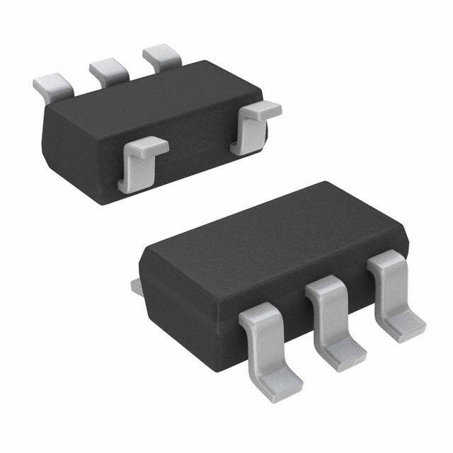
| 描述 | IC GATE AND 1CH 2-INP SC-70-5逻辑门 Sgl 2Inp Pos-AND Gate |
| 产品分类 | |
| 品牌 | Texas Instruments |
| 产品手册 | |
| 产品图片 |
|
| rohs | 符合RoHS无铅 / 符合限制有害物质指令(RoHS)规范要求 |
| 产品系列 | 逻辑集成电路,逻辑门,Texas Instruments SN74AHC1G09DCKR74AHC |
| 数据手册 | |
| 产品型号 | SN74AHC1G09DCKR |
| PCN设计/规格 | |
| 不同V、最大CL时的最大传播延迟 | 7.5ns @ 5V,50pF |
| 产品 | AND |
| 产品种类 | Logic - Gates |
| 供应商器件封装 | SC-70-5 |
| 其它名称 | 296-29203-2 |
| 包装 | 带卷 (TR) |
| 商标 | Texas Instruments |
| 安装类型 | 表面贴装 |
| 安装风格 | SMD/SMT |
| 封装 | Reel |
| 封装/外壳 | 6-TSSOP(5 引线),SC-88A,SOT-353 |
| 封装/箱体 | SC-70-5 |
| 工作温度 | -55°C ~ 125°C |
| 工厂包装数量 | 3000 |
| 最大工作温度 | + 125 C |
| 栅极数量 | 1 |
| 标准包装 | 3,000 |
| 特性 | 开路漏极 |
| 电压-电源 | 2 V ~ 5.5 V |
| 电流-输出高,低 | -,8mA |
| 电流-静态(最大值) | 1µA |
| 电源电压-最大 | 5.5 V |
| 电源电压-最小 | 2 V |
| 电路数 | 1 |
| 系列 | SN74AHC1G09 |
| 输入数 | 2 |
| 输出电压 | 5.5 V |
| 输出电流 | 25 mA |
| 逻辑电平-低 | 0.5 V ~ 1.65 V |
| 逻辑电平-高 | 1.5 V ~ 3.85 V |
| 逻辑类型 | 与门 |


PDF Datasheet 数据手册内容提取
Product Sample & Technical Tools & Support & Reference Folder Buy Documents Software Community Design SN74AHC1G09 SCLS724D–MAY2011–REVISEDSEPTEMBER2016 SN74AHC1G09 Single 2–Input Positive-AND Gate With Open-Drain Output 1 Features 3 Description • OperatingRangefrom2Vto5.5V The SN74AHC1G09 is a single 2-input positive-AND 1 gate with an open drain output configuration. The • Maximumt of6nsat5V pd deviceperformstheBooleanlogicY=A× Bor • ±8-mAOutputDriveat5V Y= A+Binpositivelogic. • Schmitt-TriggerActionatAllInputsMakesthe CircuitTolerantforSlowerInputRiseandFall DeviceInformation(1) Time PARTNUMBER PACKAGE BODYSIZE(NOM) • Latch-UpPerformanceExceeds250mAPer SN74AHC1G09DBVR SOT-23(5) 2.90mm×1.60mm JESD17 SN74AHC1G09DCKR SC70(5) 2.00mm×1.25mm • ESDProtectionExceedsJESD22: (1) For all available packages, see the orderable addendum at – 2000-VHuman-BodyModel(A114-A) theendofthedatasheet. – 1000-VCharged-DeviceModel(C101) LogicDiagram 1 2 Applications A 4 • BarcodeScanners 2 Y B • CableSolutions • E-Books • EmbeddedPCs • FieldTransmitter:TemperatureorPressure Sensors • FingerprintBiometrics • HVAC:Heating,Ventilating,andAirConditioning • Network-AttachedStorage(NAS) • ServerMotherboardandPSU • SoftwareDefinedRadios(SDR) • TV:HighDefinition(HDTV),LCD,andDigital • VideoCommunicationsSystems • WirelessDataAccessCards,Headsets, Keyboards,Mice,andLANCards 1 An IMPORTANT NOTICE at the end of this data sheet addresses availability, warranty, changes, use in safety-critical applications, intellectualpropertymattersandotherimportantdisclaimers.PRODUCTIONDATA.
SN74AHC1G09 SCLS724D–MAY2011–REVISEDSEPTEMBER2016 www.ti.com Table of Contents 1 Features.................................................................. 1 8.2 FunctionalBlockDiagram.........................................7 2 Applications........................................................... 1 8.3 FeatureDescription...................................................7 3 Description............................................................. 1 8.4 DeviceFunctionalModes..........................................7 4 RevisionHistory..................................................... 2 9 ApplicationandImplementation.......................... 8 9.1 ApplicationInformation..............................................8 5 PinConfigurationandFunctions......................... 3 9.2 TypicalApplication ...................................................8 6 Specifications......................................................... 3 10 PowerSupplyRecommendations....................... 9 6.1 AbsoluteMaximumRatings......................................3 11 Layout..................................................................... 9 6.2 ESDRatings ............................................................3 6.3 RecommendedOperatingConditions.......................4 11.1 LayoutGuidelines...................................................9 6.4 ThermalInformation..................................................4 11.2 LayoutExample......................................................9 6.5 ElectricalCharacteristics...........................................4 12 DeviceandDocumentationSupport................. 10 6.6 SwitchingCharacteristics,V =3.3V±0.3V........5 12.1 DocumentationSupport........................................10 CC 6.7 SwitchingCharacteristics,V =5V±0.5V...........5 12.2 ReceivingNotificationofDocumentationUpdates10 CC 6.8 OperatingCharacteristics..........................................5 12.3 CommunityResources..........................................10 6.9 TypicalCharacteristics..............................................5 12.4 Trademarks...........................................................10 7 ParameterMeasurementInformation..................6 12.5 ElectrostaticDischargeCaution............................10 12.6 Glossary................................................................10 8 DetailedDescription.............................................. 7 13 Mechanical,Packaging,andOrderable 8.1 Overview...................................................................7 Information........................................................... 10 4 Revision History NOTE:Pagenumbersforpreviousrevisionsmaydifferfrompagenumbersinthecurrentversion. ChangesfromRevisionC(January2016)toRevisionD Page • Deleted200-VMachineModelfromFeatures....................................................................................................................... 1 • ChangeddescriptionforpinAfromNoconnectiontoInput................................................................................................... 3 • AddedReceivingNotificationofDocumentationUpdatessection....................................................................................... 10 ChangesfromRevisionB(July2011)toRevisionC Page • AddedESDRatingstable,FeatureDescriptionsection,DeviceFunctionalModes,ApplicationandImplementation section,PowerSupplyRecommendationssection,Layoutsection,DeviceandDocumentationSupportsection,and Mechanical,Packaging,andOrderableInformationsection.................................................................................................. 1 2 SubmitDocumentationFeedback Copyright©2011–2016,TexasInstrumentsIncorporated ProductFolderLinks:SN74AHC1G09
SN74AHC1G09 www.ti.com SCLS724D–MAY2011–REVISEDSEPTEMBER2016 5 Pin Configuration and Functions DBVPackage 5-PinSOT-23 DCKPackage TopView 5-PinSC70 TopView A 1 5 VCC A 1 5 VCC B 2 B 2 GND 3 4 Y GND 3 4 Y Not to scale Not to scale PinFunctions(1) PIN I/O DESCRIPTION NAME NO. A 1 I Input B 2 I Input GND 3 — Ground V 5 — Powerpin CC Y 4 O Output (1) SeeMechanical,Packaging,andOrderableInformationfordimensions. 6 Specifications 6.1 Absolute Maximum Ratings overoperatingfree-airtemperaturerange(unlessotherwisenoted)(1) MIN MAX UNIT V Supplyvoltage –0.5 7 V CC V Inputvoltage(2) –0.5 7 V I V Outputvoltage(2) –0.5 V +0.7 V O CC I Inputclampcurrent(V <0) –20 mA IK I I Outputclampcurrent(V <0orV >V ) –20 mA OK O O CC I Continuousoutputcurrent(V =0toV ) –25 +25 mA O O CC ContinuouscurrentthroughV orGND –50 +50 mA CC T Maximumjunctiontemperature 150 °C J T Storagetemperature –65 150 °C stg (1) StressesbeyondthoselistedunderAbsoluteMaximumRatingsmaycausepermanentdamagetothedevice.Thesearestressratings only,whichdonotimplyfunctionaloperationofthedeviceattheseoranyotherconditionsbeyondthoseindicatedunderRecommended OperatingConditions.Exposuretoabsolute-maximum-ratedconditionsforextendedperiodsmayaffectdevicereliability. (2) Theinputandoutputvoltageratingsmaybeexceedediftheinputandoutputcurrentratingsareobserved. 6.2 ESD Ratings VALUE UNIT Human-bodymodel(HBM),perANSI/ESDA/JEDECJS-001(1) ±2500 V Electrostaticdischarge V (ESD) Charged-devicemodel(CDM),perJEDECspecificationJESD22-C101(2) ±1000 (1) JEDECdocumentJEP155statesthat500-VHBMallowssafemanufacturingwithastandardESDcontrolprocess. (2) JEDECdocumentJEP157statesthat250-VCDMallowssafemanufacturingwithastandardESDcontrolprocess. Copyright©2011–2016,TexasInstrumentsIncorporated SubmitDocumentationFeedback 3 ProductFolderLinks:SN74AHC1G09
SN74AHC1G09 SCLS724D–MAY2011–REVISEDSEPTEMBER2016 www.ti.com 6.3 Recommended Operating Conditions overoperatingfree-airtemperaturerange(unlessotherwisenoted) (1) MIN MAX UNIT V Supplyvoltage 2 5.5 V CC V =2V 1.5 CC V High-levelinputvoltage V =3V 2.1 V IH CC V =5.5V 3.85 CC V =2V 0.5 CC V Low-levelinputvoltage V =3V 0.9 V IL CC V =5.5V 1.65 CC V Inputvoltage 0 5.5 V I V Outputvoltage 0 5.5 V O V =2V 50 µA CC I Low-leveloutputcurrent V =3.3V±0.3V 4 OL CC mA V =5V±0.5V 8 CC V =3.3V±0.3V 100 CC Δt/Δv Inputtransitionriseorfallrate ns/V V =5V±0.5V 20 CC T Operatingfree-airtemperature –55 125 °C A (1) AllunusedinputsofthedevicemustbeheldatV orGNDtoensureproperdeviceoperation.SeeImplicationsofSloworFloating CC CMOSInputs,SCBA004. 6.4 Thermal Information SN74AHC1G09 THERMALMETRIC(1) DBV(SOT-23) DCK(SC70) UNIT 5PINS 5PINS RθJA Junction-to-ambientthermalresistance 206 252 °C/W (1) Formoreinformationabouttraditionalandnewthermalmetrics,seetheSemiconductorandICPackageThermalMetricsapplication report. 6.5 Electrical Characteristics overoperatingfree-airtemperaturerange(unlessotherwisenoted) PARAMETER TESTCONDITIONS V T MIN TYP MAX UNIT CC A 2V 0.1 I =50µA 3V 0.1 OL 4.5V 0.1 T =25°C 0.36 A V I =4mA 3V T =–40°Cto+85°C 0.44 V OL OL A T =–55°Cto+125°C 0.55 A T =25°C 0.36 A I =8mA 4.5V T =–40°Cto+85°C 0.44 OL A T =–55°Cto+125°C 0.55 A T =25°C ±0.1 A I V =5.5VorGND 0Vto5.5V T =–40°Cto+85°C ±1 µA I I A T =–55°Cto+125°C ±2 A T =25°C 1 A I V =V orGND,I =0 5.5V T =–40°Cto+85°C 10 µA CC I CC O A T =–55°Cto+125°C 20 A T =25°C 4 10 A C V =V orGND 5V pF i I CC T =–55°Cto+125°C 10 A 4 SubmitDocumentationFeedback Copyright©2011–2016,TexasInstrumentsIncorporated ProductFolderLinks:SN74AHC1G09
SN74AHC1G09 www.ti.com SCLS724D–MAY2011–REVISEDSEPTEMBER2016 6.6 Switching Characteristics, V = 3.3 V ± 0.3 V CC overrecommendedoperatingfree-airtemperaturerange,V =3.3V±0.3V(unlessotherwisenoted)(seeFigure2) CC FROM TO OUTPUT PARAMETER T MIN TYP MAX UNIT (INPUT) (OUTPUT) CAPACITANCE A T =25°C 3.6 7 A AorB Y C =15pF T =–40°Cto+85°C 1 8 ns L A T =–55°Cto+125°C 1 8.5 A t PD T =25°C 6.5 11 A AorB Y C =50pF T =–40°Cto+85°C 1.5 12 ns L A T =–55°Cto+125°C 1.5 12.5 A 6.7 Switching Characteristics, V = 5 V ± 0.5 V CC overrecommendedoperatingfree-airtemperaturerange,V =5V±0.5V(unlessotherwisenoted)(seeFigure2) CC FROM TO OUTPUT PARAMETER T MIN TYP MAX UNIT (INPUT) (OUTPUT) CAPACITANCE A T =25°C 2.5 5 A AorB Y C =15pF T =–40°Cto+85°C 1 6 ns L A T =–55°Cto+125°C 1 6.5 A t PD T =25°C 4.6 7.5 A AorB Y C =50pF T =–40°Cto+85°C 1.5 8 ns L A T =–55°Cto+125°C 1.5 8.5 A 6.8 Operating Characteristics V =5V,T =25°C CC A PARAMETER TESTCONDITIONS TYP UNIT C Powerdissipationcapacitance Noload,f=1MHz 5 pF pd 6.9 Typical Characteristics 5 4 V) Voltage ( 3 Signal 2 1 0 0 5 10 15 20 25 30 35 40 45 50 Time (ns) C001 Figure1.TPDAcrossV at25°C CC Copyright©2011–2016,TexasInstrumentsIncorporated SubmitDocumentationFeedback 5 ProductFolderLinks:SN74AHC1G09
SN74AHC1G09 SCLS724D–MAY2011–REVISEDSEPTEMBER2016 www.ti.com 7 Parameter Measurement Information VCC From Output Test From Output RL= 1 kΩ S1 Open TEST S1 UnderTest Point UnderTest GND tPLH/tPHL Open CL CL tPLZ/tPZL VCC (see NoteA) (see NoteA) tPHZ/tPZH GND Open Drain VCC LOAD CIRCUIT FOR LOAD CIRCUIT FOR TOTEM-POLE OUTPUTS 3-STATEAND OPEN-DRAIN OUTPUTS VCC Timing Input 50% VCC tw th 0 V VCC tsu VCC Input 50% VCC 50% VCC Data Input 50% VCC 50% VCC 0 V 0 V VOLTAGEWAVEFORMS VOLTAGEWAVEFORMS PULSEDURATION SETUPAND HOLD TIMES VCC Output VCC Input 50% VCC 50% VCC Control 50% VCC 50% VCC 0 V 0 V tPLH tPHL tPZL tPLZ Output VOH Waveform 1 ≈VCC InO-Puhtapsuet 50%VCC 50% VCC S1 at VCC 50% VCC VOL+0.3V VOL (see Note B) VOL tPHL tPLH tPZH tPHZ Output Out-ofO-Puhtapsuet 50% VCC 50% VCVVCOOHL (WseSae1v eNaftoo GtremN B D2) 50% VCC VOH−0.3V V≈0O HV VOLTAGEWAVEFORMS VOLTAGEWAVEFORMS PROPAGATIONDELAYTIMES ENABLEAND DISABLE TIMES INVERTINGAND NONINVERTING OUTPUTS LOW-AND HIGH-LEVELENABLING A. C includesprobeandjigcapacitance. L B. Waveform1 is for an outputwith internalconditions such that theoutputis lowexceptwhendisabledby theoutput control.Waveform2isforanoutputwithinternalconditionssuchthattheoutputishighexceptwhendisabledbythe outputcontrol. C. Allinputpulsesaresuppliedbygeneratorshavingthefollowingcharacteristics:PRR≤1MHz,Z =50Ω,t ≤3ns, O r t ≤3ns. f D. Theoutputsaremeasuredoneatatimewithoneinputtransitionpermeasurement. E. Allparametersandwaveformsarenotapplicabletoalldevices. F. Sincethisdevicehasopen-drainoutputs,t andt arethesameast . PLZ PZL PD G. t ismeasuredatV /2. PZL CC H. t ismeasuredatV +0.3V. PLZ OL Figure2. LoadCircuitandVoltageWaveforms 6 SubmitDocumentationFeedback Copyright©2011–2016,TexasInstrumentsIncorporated ProductFolderLinks:SN74AHC1G09
SN74AHC1G09 www.ti.com SCLS724D–MAY2011–REVISEDSEPTEMBER2016 8 Detailed Description 8.1 Overview The SN74AHC1G09 device contains one open-drain positive-AND gate with a maximum sink current of 8 mA. A wide operating range of 2 V to 5.5 V enables this device to be used in many different systems, and a low t pd qualifiesthisdevicetobeusedinhigh-speedapplications. 8.2 Functional Block Diagram 1 A 4 2 Y B 8.3 Feature Description The wide operating voltage range of 2 V to 5 V allows the SN74AHC1G09 to be used in systems with many different voltage rails. In addition, the voltage tolerance on the output allows the device to be used for inverting up-translation or down-translation. The device is also equipped with Schmitt-trigger inputs, which increase the abilityofthedevicetorejectnoise. 8.4 Device Functional Modes Table1liststhefunctionalmodesoftheSN74AHC1G09. Table1.FunctionTable INPUTS OUTPUT A B Y H H H(Z) L X L X L L Copyright©2011–2016,TexasInstrumentsIncorporated SubmitDocumentationFeedback 7 ProductFolderLinks:SN74AHC1G09
SN74AHC1G09 SCLS724D–MAY2011–REVISEDSEPTEMBER2016 www.ti.com 9 Application and Implementation NOTE Information in the following applications sections is not part of the TI component specification, and TI does not warrant its accuracy or completeness. TI’s customers are responsible for determining suitability of components for their purposes. Customers should validateandtesttheirdesignimplementationtoconfirmsystemfunctionality. 9.1 Application Information The SN74AHC1G09 is used in the following example in a basic power sequencing configuration. Power sequencing is often used in applications that require a processor or other delicate device with specific voltage timingrequirementsinordertoprotectthedevicefrommalfunctioning. 9.2 Typical Application VCC = 5 V A Temp. Y EN Sensor B MCU (MSP43x) VO Figure3. TypicalApplicationDiagram 9.2.1 DesignRequirements This device uses CMOS technology. Take care to avoid bus contention because it can drive currents that would exceed maximum limits. The high drive will also create fast edges into light loads so routing and load conditions shouldbeconsideredtopreventringing. 9.2.2 DetailedDesignProcedure 1. RecommendedInputConditions: – Risetimeandfalltimespecifications.See(Δt/ΔV)inRecommendedOperatingConditions. – Specifiedhighandlowlevels.See(V andV )inRecommendedOperatingConditions. IH IL – Inputsareovervoltage-tolerant,allowingthemtogoashighas(V maximum)inRecommendedOperating I ConditionsatanyvalidV . CC 2. AbsoluteMaximumConditions: – Load currents should not exceed (I maximum) per output and should not exceed (Continuous current O throughV orGND)totalcurrentforthepart.TheselimitsarelocatedinAbsoluteMaximumRatings. CC – OutputsshouldnotbepulledaboveV . CC 8 SubmitDocumentationFeedback Copyright©2011–2016,TexasInstrumentsIncorporated ProductFolderLinks:SN74AHC1G09
SN74AHC1G09 www.ti.com SCLS724D–MAY2011–REVISEDSEPTEMBER2016 Typical Application (continued) 9.2.3 ApplicationCurve 5.5 V HC 5 V VI 4.5 V AC 4 V AHC1G09 3.5 V 3 V 2.5 V 2 V 1.5 V 1 V 0.5 V 0 V –1 V –1.5 V 0 2 4 6 8 10 12 14 16 18 20 Time (ns) V =5V,Load=50Ω/50pF CC Figure4. I vsInputVoltage CC 10 Power Supply Recommendations The power supply can be any voltage between the minimum and maximum supply voltage rating located in RecommendedOperatingConditions. Each V pin should have a good bypass capacitor to prevent power disturbance. For devices with a single CC supply, a 0.1-μF capacitor is recommended; if there are multiple V pins then a 0.01-μF or 0.022-μF capacitor is CC recommended for each power pin. It is acceptable to parallel multiple bypass caps to reject different frequencies of noise. 0.1-μF and 1-μF capacitors are commonly used in parallel. The bypass capacitor should be installed as closetothepowerpinaspossibleforbestresults. 11 Layout 11.1 Layout Guidelines Whenusingmultiplebitlogicdevices,inputsmustnoteverfloat.Inmanycases,functionsorpartsoffunctionsof digital logic devices are unused (for example, when only two inputs of a triple-input AND gate are used, or only 3 of the 4 buffer gates are used). Such input pins must not be left unconnected because the undefined voltages at theoutsideconnectionsresultinundefinedoperationalstates. Thefollowingaretherulesthatmustbeobservedunderallcircumstances: • All unused inputs of digital logic devices must be connected to a high or low bias to prevent them from floating. • The logic level that should be applied to any particular unused input depends on the function of the device. GenerallytheywillbetiedtoGNDorV ,whichevermakemoresenseorismoreconvenient. CC 11.2 Layout Example VCC Input Unused Input Output Unused Input Output Input Figure5. LayoutDiagram Copyright©2011–2016,TexasInstrumentsIncorporated SubmitDocumentationFeedback 9 ProductFolderLinks:SN74AHC1G09
SN74AHC1G09 SCLS724D–MAY2011–REVISEDSEPTEMBER2016 www.ti.com 12 Device and Documentation Support 12.1 Documentation Support 12.1.1 RelatedDocumentation Forrelateddocumentation,seethefollowing: • IntroductiontoLogic,SLVA700 • ImplicationsofSloworFloatingCMOSInputs,SCBA004 12.2 Receiving Notification of Documentation Updates To receive notification of documentation updates, navigate to the device product folder on ti.com. In the upper right corner, click on Alert me to register and receive a weekly digest of any product information that has changed.Forchangedetails,reviewtherevisionhistoryincludedinanyreviseddocument. 12.3 Community Resources The following links connect to TI community resources. Linked contents are provided "AS IS" by the respective contributors. They do not constitute TI specifications and do not necessarily reflect TI's views; see TI's Terms of Use. TIE2E™OnlineCommunity TI'sEngineer-to-Engineer(E2E)Community.Createdtofostercollaboration amongengineers.Ate2e.ti.com,youcanaskquestions,shareknowledge,exploreideasandhelp solveproblemswithfellowengineers. DesignSupport TI'sDesignSupport QuicklyfindhelpfulE2Eforumsalongwithdesignsupporttoolsand contactinformationfortechnicalsupport. 12.4 Trademarks E2EisatrademarkofTexasInstruments. Allothertrademarksarethepropertyoftheirrespectiveowners. 12.5 Electrostatic Discharge Caution Thesedeviceshavelimitedbuilt-inESDprotection.Theleadsshouldbeshortedtogetherorthedeviceplacedinconductivefoam duringstorageorhandlingtopreventelectrostaticdamagetotheMOSgates. 12.6 Glossary SLYZ022—TIGlossary. Thisglossarylistsandexplainsterms,acronyms,anddefinitions. 13 Mechanical, Packaging, and Orderable Information The following pages include mechanical, packaging, and orderable information. This information is the most current data available for the designated devices. This data is subject to change without notice and revision of thisdocument.Forbrowserbasedversionsofthisdatasheet,refertothelefthandnavigation. 10 SubmitDocumentationFeedback Copyright©2011–2016,TexasInstrumentsIncorporated ProductFolderLinks:SN74AHC1G09
PACKAGE OPTION ADDENDUM www.ti.com 4-Apr-2019 PACKAGING INFORMATION Orderable Device Status Package Type Package Pins Package Eco Plan Lead/Ball Finish MSL Peak Temp Op Temp (°C) Device Marking Samples (1) Drawing Qty (2) (6) (3) (4/5) SN74AHC1G09DBVR ACTIVE SOT-23 DBV 5 3000 Green (RoHS CU NIPDAU | CU SN Level-1-260C-UNLIM -55 to 125 (A093, A09G, A09J) & no Sb/Br) SN74AHC1G09DCKR ACTIVE SC70 DCK 5 3000 Green (RoHS CU NIPDAU | CU SN Level-1-260C-UNLIM -55 to 125 (AJ3, AJG, AJJ) & no Sb/Br) (1) The marketing status values are defined as follows: ACTIVE: Product device recommended for new designs. LIFEBUY: TI has announced that the device will be discontinued, and a lifetime-buy period is in effect. NRND: Not recommended for new designs. Device is in production to support existing customers, but TI does not recommend using this part in a new design. PREVIEW: Device has been announced but is not in production. Samples may or may not be available. OBSOLETE: TI has discontinued the production of the device. (2) RoHS: TI defines "RoHS" to mean semiconductor products that are compliant with the current EU RoHS requirements for all 10 RoHS substances, including the requirement that RoHS substance do not exceed 0.1% by weight in homogeneous materials. Where designed to be soldered at high temperatures, "RoHS" products are suitable for use in specified lead-free processes. TI may reference these types of products as "Pb-Free". RoHS Exempt: TI defines "RoHS Exempt" to mean products that contain lead but are compliant with EU RoHS pursuant to a specific EU RoHS exemption. Green: TI defines "Green" to mean the content of Chlorine (Cl) and Bromine (Br) based flame retardants meet JS709B low halogen requirements of <=1000ppm threshold. Antimony trioxide based flame retardants must also meet the <=1000ppm threshold requirement. (3) MSL, Peak Temp. - The Moisture Sensitivity Level rating according to the JEDEC industry standard classifications, and peak solder temperature. (4) There may be additional marking, which relates to the logo, the lot trace code information, or the environmental category on the device. (5) Multiple Device Markings will be inside parentheses. Only one Device Marking contained in parentheses and separated by a "~" will appear on a device. If a line is indented then it is a continuation of the previous line and the two combined represent the entire Device Marking for that device. (6) Lead/Ball Finish - Orderable Devices may have multiple material finish options. Finish options are separated by a vertical ruled line. Lead/Ball Finish values may wrap to two lines if the finish value exceeds the maximum column width. Important Information and Disclaimer:The information provided on this page represents TI's knowledge and belief as of the date that it is provided. TI bases its knowledge and belief on information provided by third parties, and makes no representation or warranty as to the accuracy of such information. Efforts are underway to better integrate information from third parties. TI has taken and continues to take reasonable steps to provide representative and accurate information but may not have conducted destructive testing or chemical analysis on incoming materials and chemicals. TI and TI suppliers consider certain information to be proprietary, and thus CAS numbers and other limited information may not be available for release. In no event shall TI's liability arising out of such information exceed the total purchase price of the TI part(s) at issue in this document sold by TI to Customer on an annual basis. Addendum-Page 1
PACKAGE OPTION ADDENDUM www.ti.com 4-Apr-2019 Addendum-Page 2
PACKAGE MATERIALS INFORMATION www.ti.com 15-Dec-2018 TAPE AND REEL INFORMATION *Alldimensionsarenominal Device Package Package Pins SPQ Reel Reel A0 B0 K0 P1 W Pin1 Type Drawing Diameter Width (mm) (mm) (mm) (mm) (mm) Quadrant (mm) W1(mm) SN74AHC1G09DBVR SOT-23 DBV 5 3000 178.0 9.0 3.3 3.2 1.4 4.0 8.0 Q3 SN74AHC1G09DBVR SOT-23 DBV 5 3000 178.0 9.0 3.23 3.17 1.37 4.0 8.0 Q3 SN74AHC1G09DBVR SOT-23 DBV 5 3000 178.0 9.2 3.3 3.23 1.55 4.0 8.0 Q3 SN74AHC1G09DCKR SC70 DCK 5 3000 178.0 9.2 2.4 2.4 1.22 4.0 8.0 Q3 SN74AHC1G09DCKR SC70 DCK 5 3000 178.0 9.0 2.4 2.5 1.2 4.0 8.0 Q3 SN74AHC1G09DCKR SC70 DCK 5 3000 178.0 9.0 2.4 2.5 1.2 4.0 8.0 Q3 PackMaterials-Page1
PACKAGE MATERIALS INFORMATION www.ti.com 15-Dec-2018 *Alldimensionsarenominal Device PackageType PackageDrawing Pins SPQ Length(mm) Width(mm) Height(mm) SN74AHC1G09DBVR SOT-23 DBV 5 3000 180.0 180.0 18.0 SN74AHC1G09DBVR SOT-23 DBV 5 3000 180.0 180.0 18.0 SN74AHC1G09DBVR SOT-23 DBV 5 3000 180.0 180.0 18.0 SN74AHC1G09DCKR SC70 DCK 5 3000 180.0 180.0 18.0 SN74AHC1G09DCKR SC70 DCK 5 3000 180.0 180.0 18.0 SN74AHC1G09DCKR SC70 DCK 5 3000 180.0 180.0 18.0 PackMaterials-Page2
None
None
PACKAGE OUTLINE DBV0005A SOT-23 - 1.45 mm max height SCALE 4.000 SMALL OUTLINE TRANSISTOR C 3.0 2.6 0.1 C 1.75 1.45 B A 1.45 MAX PIN 1 INDEX AREA 1 5 2X 0.95 3.05 2.75 1.9 1.9 2 4 3 0.5 5X 0.3 0.15 0.2 C A B (1.1) TYP 0.00 0.25 GAGE PLANE 0.22 TYP 0.08 8 TYP 0.6 0 0.3 TYP SEATING PLANE 4214839/D 11/2018 NOTES: 1. All linear dimensions are in millimeters. Any dimensions in parenthesis are for reference only. Dimensioning and tolerancing per ASME Y14.5M. 2. This drawing is subject to change without notice. 3. Refernce JEDEC MO-178. 4. Body dimensions do not include mold flash, protrusions, or gate burrs. Mold flash, protrusions, or gate burrs shall not exceed 0.15 mm per side. www.ti.com
EXAMPLE BOARD LAYOUT DBV0005A SOT-23 - 1.45 mm max height SMALL OUTLINE TRANSISTOR PKG 5X (1.1) 1 5 5X (0.6) SYMM (1.9) 2 2X (0.95) 3 4 (R0.05) TYP (2.6) LAND PATTERN EXAMPLE EXPOSED METAL SHOWN SCALE:15X SOLDER MASK SOLDER MASK METAL UNDER METAL OPENING OPENING SOLDER MASK EXPOSED METAL EXPOSED METAL 0.07 MAX 0.07 MIN ARROUND ARROUND NON SOLDER MASK SOLDER MASK DEFINED DEFINED (PREFERRED) SOLDER MASK DETAILS 4214839/D 11/2018 NOTES: (continued) 5. Publication IPC-7351 may have alternate designs. 6. Solder mask tolerances between and around signal pads can vary based on board fabrication site. www.ti.com
EXAMPLE STENCIL DESIGN DBV0005A SOT-23 - 1.45 mm max height SMALL OUTLINE TRANSISTOR PKG 5X (1.1) 1 5 5X (0.6) SYMM 2 (1.9) 2X(0.95) 3 4 (R0.05) TYP (2.6) SOLDER PASTE EXAMPLE BASED ON 0.125 mm THICK STENCIL SCALE:15X 4214839/D 11/2018 NOTES: (continued) 7. Laser cutting apertures with trapezoidal walls and rounded corners may offer better paste release. IPC-7525 may have alternate design recommendations. 8. Board assembly site may have different recommendations for stencil design. www.ti.com
IMPORTANTNOTICEANDDISCLAIMER TIPROVIDESTECHNICALANDRELIABILITYDATA(INCLUDINGDATASHEETS),DESIGNRESOURCES(INCLUDINGREFERENCE DESIGNS),APPLICATIONOROTHERDESIGNADVICE,WEBTOOLS,SAFETYINFORMATION,ANDOTHERRESOURCES“ASIS” ANDWITHALLFAULTS,ANDDISCLAIMSALLWARRANTIES,EXPRESSANDIMPLIED,INCLUDINGWITHOUTLIMITATIONANY IMPLIEDWARRANTIESOFMERCHANTABILITY,FITNESSFORAPARTICULARPURPOSEORNON-INFRINGEMENTOFTHIRD PARTYINTELLECTUALPROPERTYRIGHTS. TheseresourcesareintendedforskilleddevelopersdesigningwithTIproducts.Youaresolelyresponsiblefor(1)selectingtheappropriate TIproductsforyourapplication,(2)designing,validatingandtestingyourapplication,and(3)ensuringyourapplicationmeetsapplicable standards,andanyothersafety,security,orotherrequirements.Theseresourcesaresubjecttochangewithoutnotice.TIgrantsyou permissiontousetheseresourcesonlyfordevelopmentofanapplicationthatusestheTIproductsdescribedintheresource.Other reproductionanddisplayoftheseresourcesisprohibited.NolicenseisgrantedtoanyotherTIintellectualpropertyrightortoanythird partyintellectualpropertyright.TIdisclaimsresponsibilityfor,andyouwillfullyindemnifyTIanditsrepresentativesagainst,anyclaims, damages,costs,losses,andliabilitiesarisingoutofyouruseoftheseresources. TI’sproductsareprovidedsubjecttoTI’sTermsofSale(www.ti.com/legal/termsofsale.html)orotherapplicabletermsavailableeitheron ti.comorprovidedinconjunctionwithsuchTIproducts.TI’sprovisionoftheseresourcesdoesnotexpandorotherwisealterTI’sapplicable warrantiesorwarrantydisclaimersforTIproducts. MailingAddress:TexasInstruments,PostOfficeBox655303,Dallas,Texas75265 Copyright©2019,TexasInstrumentsIncorporated