ICGOO在线商城 > 集成电路(IC) > 接口 - 模拟开关,多路复用器,多路分解器 > SN74AUC2G66YZPR
 Datasheet下载
- 型号: SN74AUC2G66YZPR
- 制造商: Texas Instruments
- 库位|库存: xxxx|xxxx
- 要求:
| 数量阶梯 | 香港交货 | 国内含税 |
| +xxxx | $xxxx | ¥xxxx |
查看当月历史价格
查看今年历史价格
SN74AUC2G66YZPR产品简介:
ICGOO电子元器件商城为您提供SN74AUC2G66YZPR由Texas Instruments设计生产,在icgoo商城现货销售,并且可以通过原厂、代理商等渠道进行代购。 SN74AUC2G66YZPR价格参考¥1.53-¥4.41。Texas InstrumentsSN74AUC2G66YZPR封装/规格:接口 - 模拟开关,多路复用器,多路分解器, 2 Circuit IC Switch 1:1 15 Ohm 8-DSBGA, 8-WCSP (1.9x0.9)。您可以下载SN74AUC2G66YZPR参考资料、Datasheet数据手册功能说明书,资料中有SN74AUC2G66YZPR 详细功能的应用电路图电压和使用方法及教程。
Texas Instruments 的 SN74AUC2G66YZPR 是一款双路 2 通道模拟开关/多路复用器,属于接口类 IC。其主要应用场景包括:

1. 信号路由:适用于需要在多个模拟或数字信号之间切换的系统,如音频、视频、传感器或多通道数据采集系统。

2. 便携式设备:该器件支持低电压操作(如0.8V至3.6V),功耗低,适合用于电池供电设备,如智能手机、平板电脑和可穿戴设备。

3. 测试与测量设备:可用于自动测试设备(ATE)中,实现多路输入信号的快速切换和选择。

4. 工业控制:在工业自动化系统中,用于切换不同传感器或执行器信号,提高系统的灵活性和集成度。

5. 通信系统:适用于通信设备中的信号路径选择,如射频前端控制、基带信号处理等。

该器件采用小型封装(如DSBGA),适合高密度PCB设计,且具备良好的导通电阻匹配性,确保信号完整性。
| 参数 | 数值 |
| 产品目录 | 集成电路 (IC)半导体 |
| 描述 | IC SWITCH DUAL 1X1 8DSBGA模拟开关 IC Dual Bilateral Analog SWCH |
| 产品分类 | |
| 品牌 | Texas Instruments |
| 产品手册 | |
| 产品图片 |
|
| rohs | 符合RoHS无铅 / 符合限制有害物质指令(RoHS)规范要求 |
| 产品系列 | 开关 IC,模拟开关 IC,Texas Instruments SN74AUC2G66YZPR74AUC |
| 数据手册 | |
| 产品型号 | SN74AUC2G66YZPR |
| PCN组件/产地 | |
| 产品目录页面 | |
| 产品种类 | 模拟开关 IC |
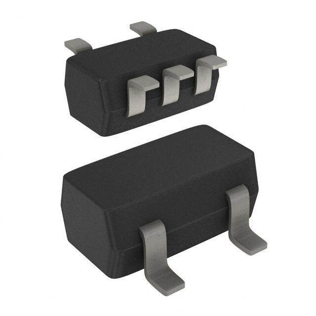
| 供应商器件封装 | 8-DSBGA,8-WCSP(1.9x0.9) |
| 其它名称 | 296-19055-1 |
| 功能 | |
| 包装 | 剪切带 (CT) |
| 单位重量 | 2.300 mg |
| 商标 | Texas Instruments |
| 安装类型 | 表面贴装 |
| 安装风格 | SMD/SMT |
| 导通电阻 | 15 欧姆 |
| 导通电阻—最大值 | 17 Ohms |
| 封装 | Reel |
| 封装/外壳 | 8-XFBGA,DSBGA |
| 封装/箱体 | DSBGA-8 |
| 工作温度 | -40°C ~ 85°C |
| 工作电源电压 | 0.8 V to 2.7 V |
| 工厂包装数量 | 3000 |
| 开关配置 | SPST |
| 最大工作温度 | + 85 C |
| 最小工作温度 | - 40 C |
| 标准包装 | 1 |
| 电压-电源,单/双 (±) | 0.8 V ~ 2.7 V |
| 电压源 | 单电源 |
| 电流-电源 | 10µA |
| 电源电压-最大 | 2.7 V |
| 电源电压-最小 | 0.8 V |
| 电源电流—最大值 | 0.01 mA |
| 电路 | 2 x SPST - NO |
| 空闲时间—最大值 | 3.4 ns |
| 系列 | SN74AUC2G66 |
| 运行时间—最大值 | 2.7 ns |


- 商务部:美国ITC正式对集成电路等产品启动337调查
- 曝三星4nm工艺存在良率问题 高通将骁龙8 Gen1或转产台积电
- 太阳诱电将投资9.5亿元在常州建新厂生产MLCC 预计2023年完工
- 英特尔发布欧洲新工厂建设计划 深化IDM 2.0 战略
- 台积电先进制程称霸业界 有大客户加持明年业绩稳了
- 达到5530亿美元!SIA预计今年全球半导体销售额将创下新高
- 英特尔拟将自动驾驶子公司Mobileye上市 估值或超500亿美元
- 三星加码芯片和SET,合并消费电子和移动部门,撤换高东真等 CEO
- 三星电子宣布重大人事变动 还合并消费电子和移动部门
- 海关总署:前11个月进口集成电路产品价值2.52万亿元 增长14.8%


PDF Datasheet 数据手册内容提取
SN74AUC2G66 DUAL BILATERAL ANALOG SWITCH www.ti.com SCES507A–NOVEMBER2003–REVISEDJANUARY2007 FEATURES DCT OR DCU PACKAGE • AvailableintheTexasInstruments (TOP VIEW) NanoFree™Package • Operatesat0.8Vto2.7V 1A 1 8 VCC • Sub-1-VOperable 1B 2 7 1C • Maxt of0.5nsat1.8V 2C 3 6 2B pd GND 4 5 2A • LowPowerConsumption,10m Aat2.7V • HighOn-OffOutputVoltageRatio • HighDegreeofLinearity YZP PACKAGE • Latch-UpPerformanceExceeds100mAPer (BOTTOM VIEW) JESD78,ClassII GND 4 5 2A • ESDPerformanceTestedPerJESD22 2C 3 6 2B – 2000-VHuman-BodyModel 1B 2 7 1C (A114-B,ClassII) 1A 1 8 VCC – 200-VMachineModel(A115-A) – 1000-VCharged-DeviceModel(C101) DESCRIPTION/ORDERING INFORMATION This dual analog switch is operational at 0.8-V to 2.7-V V , but is designed specifically for 1.1-V to 2.7-V V CC CC operation. The SN74AUC2G66 can handle both analog and digital signals. It permits signals with amplitudes of up to 2.7-V (peak)tobetransmittedineitherdirection. NanoFree™ package technology is a major breakthrough in IC packaging concepts, using the die as the package. Applications include signal gating, chopping, modulation or demodulation (modem), and signal multiplexing for analog-to-digitalanddigital-to-analogconversionsystems. ORDERINGINFORMATION T PACKAGE(1) ORDERABLEPARTNUMBER TOP-SIDEMARKING(2) A NanoFree™–WCSP(DSBGA) Reelof3000 SN74AUC2G66YZPR ___U6_ 0.23-mmLargeBump–YZP(Pb-free) –40(cid:176) Cto85(cid:176) C SSOP–DCT Reelof3000 SN74AUC2G66DCTR U66___ VSSOP–DCU Reelof3000 SN74AUC2G66DCUR U66_ (1) Packagedrawings,standardpackingquantities,thermaldata,symbolization,andPCBdesignguidelinesareavailableat www.ti.com/sc/package. (2) DCT:Theactualtop-sidemarkinghasthreeadditionalcharactersthatdesignatetheyear,month,andassembly/testsite. DCU:Theactualtop-sidemarkinghasoneadditionalcharacterthatdesignatestheassembly/testsite. YZP:Theactualtop-sidemarkinghasthreeprecedingcharacterstodenoteyear,month,andsequencecode,andonefollowing charactertodesignatetheassembly/testsite.Pin1identifierindicatessolder-bumpcomposition(1=SnPb,•=Pb-free). FUNCTIONTABLE CONTROL INPUT SWITCH (C) L OFF H ON Pleasebeawarethatanimportantnoticeconcerningavailability,standardwarranty,anduseincriticalapplicationsofTexas Instrumentssemiconductorproductsanddisclaimerstheretoappearsattheendofthisdatasheet. NanoFreeisatrademarkofTexasInstruments. PRODUCTIONDATAinformationiscurrentasofpublicationdate. Copyright©2003–2007,TexasInstrumentsIncorporated Products conform to specifications per the terms of the Texas Instruments standard warranty. Production processing does not necessarilyincludetestingofallparameters.
SN74AUC2G66 DUAL BILATERAL ANALOG SWITCH www.ti.com SCES507A–NOVEMBER2003–REVISEDJANUARY2007 LOGICDIAGRAM(POSITIVELOGIC) 1 2 A B 4 C Absolute Maximum Ratings(1) overoperatingfree-airtemperaturerange(unlessotherwisenoted) MIN MAX UNIT V Supplyvoltagerange(2) –0.5 3.6 V CC V Inputvoltagerange(2)(3) –0.5 3.6 V I V SwitchI/Ovoltagerange (2)(3) –0.5 V +0.5 V I/O CC I Controlinputclampcurrent V <0 –50 mA IK I I I/Oportdiodecurrent V <0orV >V – 50 mA IOK I/O I/O CC I On-stateswitchcurrent V =0toV – 50 mA T I/O CC ContinuouscurrentthroughV orGND – 100 mA CC DCTpackage 220 q Packagethermalimpedance(4) DCUpackage 227 (cid:176) C/W JA YZPpackage 102 T Storagetemperaturerange –65 150 (cid:176) C stg (1) Stressesbeyondthoselistedunder"absolutemaximumratings"maycausepermanentdamagetothedevice.Thesearestressratings only,andfunctionaloperationofthedeviceattheseoranyotherconditionsbeyondthoseindicatedunder"recommendedoperating conditions"isnotimplied.Exposuretoabsolute-maximum-ratedconditionsforextendedperiodsmayaffectdevicereliability. (2) Allvoltagesarewithrespecttogroundunlessotherwisespecified. (3) Theinputnegative-voltageandoutputvoltageratingsmaybeexceedediftheinputandoutputcurrentratingsareobserved. (4) ThepackagethermalimpedanceiscalculatedinaccordancewithJESD51-7. 2 SubmitDocumentationFeedback
SN74AUC2G66 DUAL BILATERAL ANALOG SWITCH www.ti.com SCES507A–NOVEMBER2003–REVISEDJANUARY2007 Recommended Operating Conditions(1) MIN MAX UNIT V Supplyvoltage 0.8 2.7 V CC V =0.8V V CC CC V High-levelinputvoltage V =1.1Vto1.95V 0.65· V V IH CC CC V =2.3Vto2.7V 1.7 CC V =0.8V 0 CC V Low-levelinputvoltage V =1.1Vto1.95V 0.35· V V IL CC CC V =2.3Vto2.7V 0.7 CC V I/Oportvoltage 0 V V I/O CC V Controlinputvoltage 0 3.6 V I V =0.8Vto1.65V(2) 20 CC D t/D v Inputtransitionriseorfallrate V =1.65Vto2.3V(3) 20 ns/V CC V =2.3Vto2.7V(3) 20 CC T Operatingfree-airtemperature –40 85 (cid:176) C A (1) AllunusedinputsofthedevicemustbeheldatV orGNDtoensureproperdeviceoperation.RefertotheTIapplicationreport, CC ImplicationsofSloworFloatingCMOSInputs,literaturenumberSCBA004. (2) ThedatawastakenatC =15pF,R =2kW (seeFigure1). L L (3) ThedatawastakenatC =30pF,R =500W (seeFigure1). L L Electrical Characteristics overrecommendedoperatingfree-airtemperaturerange(unlessotherwisenoted) PARAMETER TESTCONDITIONS V MIN TYP(1) MAX UNIT CC 1.1V 17 40 r On-stateswitchresistance VVI==VVCCorGND, IS=4mA 1.65V 7 20 W on C IH (seeFigure1andFigure2) I =8mA 2.3V 4 15 S 1.1V 131 180 r Peakonresistance VVI==VVCCtoGND, IS=4mA 1.65V 32 80 W on(p) C IH (seeFigure1andFigure2) I =8mA 2.3V 15 20 S 1.1V 3 D r Donif-fsetraetnecreesoifstance VVI==VVCCtoGND, IS=4mA 1.65V 1 W on C IH betweenswitches (seeFigure1andFigure2) I =8mA 2.3V 1 S V =V andV =GND,or – 1 I CC O I Off-stateswitchleakagecurrent V =GNDandV =V , 2.7V m A S(off) VI =V (seeFigOure3C)C – 0.1(2) C IL I On-stateswitchleakagecurrent VI=VCCorGND,VC=VIH,VO=Open 2.7V – 1 m A S(on) (seeFigure4) – 0.1(2) I Controlinputcurrent V =V orGND 0to2.7V ±5 m A I I CC I Supplycurrent V =V orGND, I =0 0.8Vto2.7V 10 m A CC I CC O C Controlinputcapacitance 2.5V 2.5 pF ic C Switchinput/outputcapacitance 2.5V 3 pF io(off) C Switchinput/outputcapacitance 2.5V 7 pF io(on) (1) t =25(cid:176) C a (2) ThedatawastakenatC =15pF,R =2kW (seeFigure1). L L SubmitDocumentationFeedback 3
SN74AUC2G66 DUAL BILATERAL ANALOG SWITCH www.ti.com SCES507A–NOVEMBER2003–REVISEDJANUARY2007 Switching Characteristics overrecommendedoperatingfree-airtemperaturerange,C =15pF(unlessotherwisenoted)(seeFigure5) L V =1.2V V =1.5V V =1.8V V =2.5V PARAMETER FROM TO VCC=0.8V C±C0.1V C±C0.1V C±C0.15V C±C0.2V UNIT (INPUT) (OUTPUT) TYP MIN MAX MIN MAX MIN TYP MAX MIN MAX t (1) AorB BorA 1 0.6 0.5 0.5 0.4 ns pd t C AorB 5 0.5 3 0.5 2.1 0.5 0.9 1.6 0.5 1.4 ns en t C AorB 5.3 0.5 4 0.5 3 0.5 2.6 3.3 0.5 2.7 ns dis (1) ThepropagationdelayisthecalculatedRCtimeconstantofthetypicalon-stateresistanceoftheswitchandthespecifiedload capacitancewhendrivenbyanidealvoltagesource(zerooutputimpedance). Switching Characteristics overrecommendedoperatingfree-airtemperaturerange,C =30pF(unlessotherwisenoted)(seeFigure5) L V =1.8V V =2.5V CC CC PARAMETER FROM TO – 0.15V – 0.2V UNIT (INPUT) (OUTPUT) MIN TYP MAX MIN MAX t (1) AorB BorA 0.7 0.7 ns pd t C AorB 0.5 1.6 2.7 0.5 2.3 ns en t C AorB 0.5 2.7 3.4 0.5 2 ns dis (1) ThepropagationdelayisthecalculatedRCtimeconstantofthetypicalon-stateresistanceoftheswitchandthespecifiedload capacitancewhendrivenbyanidealvoltagesource(zerooutputimpedance). Analog Switch Characteristics T =25(cid:176) C A FROM TO PARAMETER TESTCONDITIONS V TYP UNIT (INPUT) (OUTPUT) CC 0.8V 101 C =50pF,R =600W , 1.1V 150 L L f =sinewave 1.4V 175 in (seeFigure6) 1.65V 250 Frequencyresponse 2.3V 400 AorB BorA MHz (switchON) 0.8V 450 C =5pF,R =50W , 1.1V >500 L L f =sinewave 1.4V >500 in (seeFigure6) 1.65V >500 2.3V >500 0.8V –60 C =50pF,R =600W , 1.1V –60 L L f =1MHz(sinewave) 1.4V –60 in (seeFigure7) 1.65V –60 Crosstalk 2.3V –60 AorB BorA dB (betweenswitches) 0.8V –65 C =5pF,R =50W , 1.1V –65 L L f =1MHz(sinewave) 1.4V –65 in (seeFigure7) 1.65V –65 2.3V –65 4 SubmitDocumentationFeedback
SN74AUC2G66 DUAL BILATERAL ANALOG SWITCH www.ti.com SCES507A–NOVEMBER2003–REVISEDJANUARY2007 Analog Switch Characteristics (continued) T =25(cid:176) C A FROM TO PARAMETER TESTCONDITIONS V TYP UNIT (INPUT) (OUTPUT) CC 0.8V 9 Crosstalk C =50pF,R =600W , 1.1V 14 L L (controlinputtosignal C AorB f =1MHz(squarewave) 1.4V 15 mV in output) (seeFigure8) 1.65V 16 2.3V 20 0.8V –50 C =50pF,R =600W , 1.1V –50 L L f =1MHz(sinewave) 1.4V –50 in (seeFigure9) 1.65V –50 Feedthroughattenuation 2.3V –50 AorB BorA dB (switchOFF) 0.8V –60 C =5pF,R =50W , 1.1V –60 L L f =1MHz(sinewave) 1.4V –60 in (seeFigure9) 1.65V –60 2.3V –60 0.8V 7 C =50pF,R =10kW , 1.1V 0.256 L L AorB BorA f =1kHz(sinewave) 1.4V 0.04 in (seeFigure10) 1.65V 0.03 2.3V 0.01 Sine-wavedistortion % 0.8V 3.7 C =50pF,R =10kW , 1.1V 0.4 L L AorB BorA f =10kHz(sinewave) 1.4V 0.04 in (seeFigure10) 1.65V 0.02 2.3V 0.02 Operating Characteristics T =25(cid:176) C A TEST VCC=0.8V VCC=1.2V VCC=1.5V VCC=1.8V VCC=2.5V PARAMETER UNIT CONDITIONS TYP TYP TYP TYP TYP Powerdissipation C f=10MHz 2.5 2.5 2.5 2.5 2.5 pF pd capacitance SubmitDocumentationFeedback 5
SN74AUC2G66 DUAL BILATERAL ANALOG SWITCH www.ti.com SCES507A–NOVEMBER2003–REVISEDJANUARY2007 PARAMETER MEASUREMENT INFORMATION VCC VCC A or B B or A VI = VCC or GND VO C VIH VC (ON) GND IS V (cid:1)V V ron(cid:2) I I O (cid:1) S VI – VO Figure1.On-StateResistanceTestCircuit 120 100 VCC = 1.1 V 80 60 40 VCC = 1.65 V 20 VCC = 2.3 V 0 0 1 2 3 Figure2.Typicalr asaFunctionofVoltage(V)forV =0toV on I I CC 6 SubmitDocumentationFeedback
SN74AUC2G66 DUAL BILATERAL ANALOG SWITCH www.ti.com SCES507A–NOVEMBER2003–REVISEDJANUARY2007 PARAMETER MEASUREMENT INFORMATION VCC VCC A or B B or A VI A VO C VIL VC (OFF) GND Condition 1: VI = GND, VO = VCC Condition 2: VI = VCC, VO = GND Figure3.Off-StateSwitchLeakage-CurrentTestCircuit VCC VCC A or B B or A VI = VCC or GND A VO VO = Open C VIH VC (ON) GND Figure4.On-StateLeakage-CurrentTestCircuit SubmitDocumentationFeedback 7
SN74AUC2G66 DUAL BILATERAL ANALOG SWITCH www.ti.com SCES507A–NOVEMBER2003–REVISEDJANUARY2007 PARAMETER MEASUREMENT INFORMATION VLOAD From Output RL S1 Open TEST S1 Under Test GND tPLH/tPHL Open (see Note CAL) RL tPLZ/tPZL VLOAD tPHZ/tPZH GND LOAD CIRCUIT INPUTS VCC VI tr/tf VM VLOAD CL RL VD 0.8 V VCC ≤2 ns VCC/2 2 × VCC 15 pF 2 kW 0.1 V 1.2 V ± 0.1 V VCC ≤2 ns VCC/2 2 × VCC 15 pF 2 kW 0.1 V 1.5 V ± 0.1 V VCC ≤2 ns VCC/2 2 × VCC 15 pF 2 kW 0.1 V 1.8 V ± 0.15 V VCC ≤2 ns VCC/2 2 × VCC 15 pF 2 kW 0.15 V 2.5 V ± 0.2 V VCC ≤2 ns VCC/2 2 × VCC 15 pF 2 kW 0.15 V 1.8 V ± 0.15 V VCC ≤2 ns VCC/2 2 × VCC 30 pF 1 kW 0.15 V 2.5 V ± 0.2 V VCC ≤2 ns VCC/2 2 × VCC 30 pF 500 W 0.15 V VI Timing Input VM 0 V tw VI tsu th VI Input VM VM Data Input VM VM 0 V 0 V VOLTAGE WAVEFORMS VOLTAGE WAVEFORMS PULSE DURATION SETUP AND HOLD TIMES VI VI Output Input VM VM Control VM VM 0 V 0 V tPLH tPHL tPZL tPLZ Output VOH Waveform 1 VLOAD/2 Output VM VM VOL (Ss1e ea tN VoLteO ABD) VM VOL + VD VOL tPHL tPLH tPZH tPHZ Output VM VM VOH WSa1v eaOfto uGrtmpNu D2t VM VOH − VD VOH VOL (see Note B) ≈0 V VOLTAGE WAVEFORMS VOLTAGE WAVEFORMS PROPAGATION DELAY TIMES ENABLE AND DISABLE TIMES INVERTING AND NONINVERTING OUTPUTS LOW- AND HIGH-LEVEL ENABLING NOTES: A. CL includes probe and jig capacitance. B. Waveform 1 is for an output with internal conditions such that the output is low, except when disabled by the output control. Waveform2 is for an output with internal conditions such that the output is high, except when disabled by the output control. C. All input pulses are supplied by generators having the following characteristics: PRR ≤ 10 MHz, ZO = 50 W , slew rate ≥ 1 V/ns. D. The outputs are measured one at a time, with one transition per measurement. E. tPLZ and tPHZ are the same as tdis. F. tPZL and tPZH are the same as ten. G. tPLH and tPHL are the same as tpd. H. All parameters and waveforms are not applicable to all devices. Figure5.LoadCircuitandVoltageWaveforms 8 SubmitDocumentationFeedback
SN74AUC2G66 DUAL BILATERAL ANALOG SWITCH www.ti.com SCES507A–NOVEMBER2003–REVISEDJANUARY2007 PARAMETER MEASUREMENT INFORMATION VCC VCC 0.1 m F A or B B or A VO fin 50 W VIH VCC RL CL (ON) GND VCC/2 RL/CL: 600 W / 50 pF RL/CL: 50 W / 5 pF Figure6.FrequencyResponse(SwitchON) VCC VCC 0.1 m F 1A or 1B 1B or 1A VO1 Rin 600 W C RL CL fin 50 W VIH VC 600 W 50 pF (On) VCC/2 2A or 2B 2B or 2A VO2 R60in0 W VIL VCC R60L0 W C50L pF (Off) GND VCC/2 20log10(VO2/VI1) or 20log10(VO1/VI2) Figure7.Crosstalk(BetweenSwitches) SubmitDocumentationFeedback 9
SN74AUC2G66 DUAL BILATERAL ANALOG SWITCH www.ti.com SCES507A–NOVEMBER2003–REVISEDJANUARY2007 PARAMETER MEASUREMENT INFORMATION VCC VCC Rin 600 W A or B B or A VCC/2 VO C RL CL 600 W 50 pF VC GND 50 W VCC/2 Figure8.Crosstalk(ControlInput–SwitchOutput) VCC VCC 0.1 m F A or B B or A VO fin 50 W RL VIL VCC RL CL (OFF) GND VCC/2 VCC/2 RL/CL: 600 W / 50 pF RL/CL: 50 W / 5 pF Figure9.Feedthrough,SwitchOff 10 SubmitDocumentationFeedback
SN74AUC2G66 DUAL BILATERAL ANALOG SWITCH www.ti.com SCES507A–NOVEMBER2003–REVISEDJANUARY2007 PARAMETER MEASUREMENT INFORMATION VCC VCC 10 m F 10 m F A or B B or A VO C RL CL fin 600 W VIH VC 10 kW 50 pF (ON) GND VCC/2 VCC = 0.8 V, VI = 0.7 VP-P VCC = 1.1 V, VI = 1 VP-P VCC = 1.4 V, VI = 1.2 VP-P VCC = 1.65 V, VI = 1.4 VP-P VCC = 2.3 V, VI = 2 VP-P Figure10.Sine-WaveDistortion SubmitDocumentationFeedback 11
PACKAGE OPTION ADDENDUM www.ti.com 20-Jun-2017 PACKAGING INFORMATION Orderable Device Status Package Type Package Pins Package Eco Plan Lead/Ball Finish MSL Peak Temp Op Temp (°C) Device Marking Samples (1) Drawing Qty (2) (6) (3) (4/5) SN74AUC2G66DCTR ACTIVE SM8 DCT 8 3000 Green (RoHS CU NIPDAU Level-1-260C-UNLIM -40 to 85 U66 & no Sb/Br) (R ~ Z) SN74AUC2G66DCUR ACTIVE VSSOP DCU 8 3000 Green (RoHS CU NIPDAU | CU SN Level-1-260C-UNLIM -40 to 85 (66 ~ U66Q ~ U66R) & no Sb/Br) (UR ~ UZ) SN74AUC2G66DCURE4 ACTIVE VSSOP DCU 8 3000 Green (RoHS CU NIPDAU Level-1-260C-UNLIM -40 to 85 U66R & no Sb/Br) SN74AUC2G66DCURG4 ACTIVE VSSOP DCU 8 3000 Green (RoHS CU NIPDAU Level-1-260C-UNLIM -40 to 85 U66R & no Sb/Br) SN74AUC2G66YZPR ACTIVE DSBGA YZP 8 3000 Green (RoHS SNAGCU Level-1-260C-UNLIM -40 to 85 U6N & no Sb/Br) (1) The marketing status values are defined as follows: ACTIVE: Product device recommended for new designs. LIFEBUY: TI has announced that the device will be discontinued, and a lifetime-buy period is in effect. NRND: Not recommended for new designs. Device is in production to support existing customers, but TI does not recommend using this part in a new design. PREVIEW: Device has been announced but is not in production. Samples may or may not be available. OBSOLETE: TI has discontinued the production of the device. (2) RoHS: TI defines "RoHS" to mean semiconductor products that are compliant with the current EU RoHS requirements for all 10 RoHS substances, including the requirement that RoHS substance do not exceed 0.1% by weight in homogeneous materials. Where designed to be soldered at high temperatures, "RoHS" products are suitable for use in specified lead-free processes. TI may reference these types of products as "Pb-Free". RoHS Exempt: TI defines "RoHS Exempt" to mean products that contain lead but are compliant with EU RoHS pursuant to a specific EU RoHS exemption. Green: TI defines "Green" to mean the content of Chlorine (Cl) and Bromine (Br) based flame retardants meet JS709B low halogen requirements of <=1000ppm threshold. Antimony trioxide based flame retardants must also meet the <=1000ppm threshold requirement. (3) MSL, Peak Temp. - The Moisture Sensitivity Level rating according to the JEDEC industry standard classifications, and peak solder temperature. (4) There may be additional marking, which relates to the logo, the lot trace code information, or the environmental category on the device. (5) Multiple Device Markings will be inside parentheses. Only one Device Marking contained in parentheses and separated by a "~" will appear on a device. If a line is indented then it is a continuation of the previous line and the two combined represent the entire Device Marking for that device. (6) Lead/Ball Finish - Orderable Devices may have multiple material finish options. Finish options are separated by a vertical ruled line. Lead/Ball Finish values may wrap to two lines if the finish value exceeds the maximum column width. Addendum-Page 1
PACKAGE OPTION ADDENDUM www.ti.com 20-Jun-2017 Important Information and Disclaimer:The information provided on this page represents TI's knowledge and belief as of the date that it is provided. TI bases its knowledge and belief on information provided by third parties, and makes no representation or warranty as to the accuracy of such information. Efforts are underway to better integrate information from third parties. TI has taken and continues to take reasonable steps to provide representative and accurate information but may not have conducted destructive testing or chemical analysis on incoming materials and chemicals. TI and TI suppliers consider certain information to be proprietary, and thus CAS numbers and other limited information may not be available for release. In no event shall TI's liability arising out of such information exceed the total purchase price of the TI part(s) at issue in this document sold by TI to Customer on an annual basis. Addendum-Page 2
PACKAGE MATERIALS INFORMATION www.ti.com 23-Nov-2017 TAPE AND REEL INFORMATION *Alldimensionsarenominal Device Package Package Pins SPQ Reel Reel A0 B0 K0 P1 W Pin1 Type Drawing Diameter Width (mm) (mm) (mm) (mm) (mm) Quadrant (mm) W1(mm) SN74AUC2G66DCTR SM8 DCT 8 3000 180.0 13.0 3.35 4.5 1.55 4.0 12.0 Q3 SN74AUC2G66DCUR VSSOP DCU 8 3000 180.0 8.4 2.25 3.35 1.05 4.0 8.0 Q3 SN74AUC2G66DCUR VSSOP DCU 8 3000 180.0 9.0 2.05 3.3 1.0 4.0 8.0 Q3 SN74AUC2G66DCURG4 VSSOP DCU 8 3000 180.0 8.4 2.25 3.35 1.05 4.0 8.0 Q3 SN74AUC2G66YZPR DSBGA YZP 8 3000 178.0 9.2 1.02 2.02 0.63 4.0 8.0 Q1 PackMaterials-Page1
PACKAGE MATERIALS INFORMATION www.ti.com 23-Nov-2017 *Alldimensionsarenominal Device PackageType PackageDrawing Pins SPQ Length(mm) Width(mm) Height(mm) SN74AUC2G66DCTR SM8 DCT 8 3000 182.0 182.0 20.0 SN74AUC2G66DCUR VSSOP DCU 8 3000 202.0 201.0 28.0 SN74AUC2G66DCUR VSSOP DCU 8 3000 182.0 182.0 20.0 SN74AUC2G66DCURG4 VSSOP DCU 8 3000 202.0 201.0 28.0 SN74AUC2G66YZPR DSBGA YZP 8 3000 220.0 220.0 35.0 PackMaterials-Page2
None
None
MECHANICAL DATA MPDS049B – MAY 1999 – REVISED OCTOBER 2002 DCT (R-PDSO-G8) PLASTIC SMALL-OUTLINE PACKAGE 0,30 0,65 0,13 M 0,15 8 5 0,15 NOM 2,90 4,25 ÇÇÇÇÇ 2,70 3,75 ÇÇÇÇÇ ÇÇÇÇÇ Gage Plane ÇÇÇÇÇ PIN 1 INDEX AREA 0,25 1 4 0°– 8° 3,15 0,60 2,75 0,20 1,30 MAX Seating Plane 0,10 0,10 0,00 4188781/C 09/02 NOTES: A. All linear dimensions are in millimeters. B. This drawing is subject to change without notice. C. Body dimensions do not include mold flash or protrusion D. Falls within JEDEC MO-187 variation DA. • POST OFFICE BOX 655303 DALLAS, TEXAS 75265
None
PACKAGE OUTLINE YZP0008 DSBGA - 0.5 mm max height SCALE 8.000 DIE SIZE BALL GRID ARRAY B E A BALL A1 CORNER D C 0.5 MAX SEATING PLANE 0.19 0.05 C 0.15 BALL TYP 0.5 TYP D C SYMM 1.5 D: Max = 1.918 mm, Min =1 .858 mm TYP B E: Max = 0.918 mm, Min =0 .858 mm 0.5 TYP A 0.25 8X 1 2 0.21 0.015 C A B SYMM 4223082/A 07/2016 NOTES: 1. All linear dimensions are in millimeters. Any dimensions in parenthesis are for reference only. Dimensioning and tolerancing per ASME Y14.5M. 2. This drawing is subject to change without notice. www.ti.com
EXAMPLE BOARD LAYOUT YZP0008 DSBGA - 0.5 mm max height DIE SIZE BALL GRID ARRAY (0.5) TYP 8X ( 0.23) 1 2 A (0.5) TYP B SYMM C D SYMM LAND PATTERN EXAMPLE SCALE:40X SOLDER MASK 0.05 MAX 0.05 MIN ( 0.23) OPENING SOLDER MASK OPENING ( 0.23) METAL METAL UNDER SOLDER MASK NON-SOLDER MASK SOLDER MASK DEFINED DEFINED (PREFERRED) SOLDER MASK DETAILS NOT TO SCALE 4223082/A 07/2016 NOTES: (continued) 3. Final dimensions may vary due to manufacturing tolerance considerations and also routing constraints. For more information, see Texas Instruments literature number SNVA009 (www.ti.com/lit/snva009). www.ti.com
EXAMPLE STENCIL DESIGN YZP0008 DSBGA - 0.5 mm max height DIE SIZE BALL GRID ARRAY (0.5) TYP 8X ( 0.25) (R0.05) TYP 1 2 A (0.5) TYP B SYMM C METAL TYP D SYMM SOLDER PASTE EXAMPLE BASED ON 0.1 mm THICK STENCIL SCALE:40X 4223082/A 07/2016 NOTES: (continued) 4. Laser cutting apertures with trapezoidal walls and rounded corners may offer better paste release. www.ti.com
IMPORTANTNOTICEANDDISCLAIMER TIPROVIDESTECHNICALANDRELIABILITYDATA(INCLUDINGDATASHEETS),DESIGNRESOURCES(INCLUDINGREFERENCE DESIGNS),APPLICATIONOROTHERDESIGNADVICE,WEBTOOLS,SAFETYINFORMATION,ANDOTHERRESOURCES“ASIS” ANDWITHALLFAULTS,ANDDISCLAIMSALLWARRANTIES,EXPRESSANDIMPLIED,INCLUDINGWITHOUTLIMITATIONANY IMPLIEDWARRANTIESOFMERCHANTABILITY,FITNESSFORAPARTICULARPURPOSEORNON-INFRINGEMENTOFTHIRD PARTYINTELLECTUALPROPERTYRIGHTS. TheseresourcesareintendedforskilleddevelopersdesigningwithTIproducts.Youaresolelyresponsiblefor(1)selectingtheappropriate TIproductsforyourapplication,(2)designing,validatingandtestingyourapplication,and(3)ensuringyourapplicationmeetsapplicable standards,andanyothersafety,security,orotherrequirements.Theseresourcesaresubjecttochangewithoutnotice.TIgrantsyou permissiontousetheseresourcesonlyfordevelopmentofanapplicationthatusestheTIproductsdescribedintheresource.Other reproductionanddisplayoftheseresourcesisprohibited.NolicenseisgrantedtoanyotherTIintellectualpropertyrightortoanythird partyintellectualpropertyright.TIdisclaimsresponsibilityfor,andyouwillfullyindemnifyTIanditsrepresentativesagainst,anyclaims, damages,costs,losses,andliabilitiesarisingoutofyouruseoftheseresources. TI’sproductsareprovidedsubjecttoTI’sTermsofSale(www.ti.com/legal/termsofsale.html)orotherapplicabletermsavailableeitheron ti.comorprovidedinconjunctionwithsuchTIproducts.TI’sprovisionoftheseresourcesdoesnotexpandorotherwisealterTI’sapplicable warrantiesorwarrantydisclaimersforTIproducts. MailingAddress:TexasInstruments,PostOfficeBox655303,Dallas,Texas75265 Copyright©2019,TexasInstrumentsIncorporated