ICGOO在线商城 > 集成电路(IC) > 接口 - 模拟开关,多路复用器,多路分解器 > DG612DY-T1-E3

 Datasheet下载
- 型号: DG612DY-T1-E3
- 制造商: Vishay
- 库位|库存: xxxx|xxxx
- 要求:
| 数量阶梯 | 香港交货 | 国内含税 |
| +xxxx | $xxxx | ¥xxxx |
查看当月历史价格
查看今年历史价格
DG612DY-T1-E3产品简介:
ICGOO电子元器件商城为您提供DG612DY-T1-E3由Vishay设计生产,在icgoo商城现货销售,并且可以通过原厂、代理商等渠道进行代购。 DG612DY-T1-E3价格参考。VishayDG612DY-T1-E3封装/规格:接口 - 模拟开关,多路复用器,多路分解器, 4 Circuit IC Switch 1:1 45 Ohm 16-SOIC。您可以下载DG612DY-T1-E3参考资料、Datasheet数据手册功能说明书,资料中有DG612DY-T1-E3 详细功能的应用电路图电压和使用方法及教程。
Vishay Siliconix 的 DG612DY-T1-E3 是一款高性能模拟开关,属于接口类器件中的模拟开关、多路复用器和多路分解器。该器件广泛应用于需要高频信号切换与低失真传输的场景。

DG612DY-T1-E3 主要用于通信系统中的信号路由控制,例如在无线基站、测试测量设备中实现射频或中频信号的切换。它也可用于音频处理设备,实现高保真音频信号的选择与切换,保证音质不失真。此外,在工业自动化控制系统中,这款器件可用于多路传感器信号的采集与选择,提高系统的灵活性与响应速度。

该器件具有低导通电阻、高隔离度和快速开关速度的特点,适合要求严苛的高频与高精度应用。因此,它也常见于医疗成像设备、精密仪器仪表等对信号完整性要求极高的领域。

总之,DG612DY-T1-E3 的应用场景涵盖通信、测试测量、音频处理、工业控制及医疗设备等多个领域,适用于各种需要高效、精准模拟信号切换的设计。
| 参数 | 数值 |
| 产品目录 | 集成电路 (IC) |
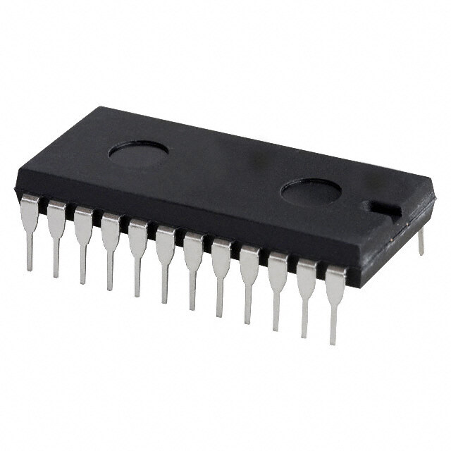
| 描述 | IC SWITCH QUAD SPST 16-SOIC |
| 产品分类 | |
| 品牌 | Vishay Siliconix |
| 数据手册 | |
| 产品图片 |
|
| 产品型号 | DG612DY-T1-E3 |
| rohs | 无铅 / 符合限制有害物质指令(RoHS)规范要求 |
| 产品系列 | - |
| 供应商器件封装 | 16-SOIC |
| 其它名称 | DG612DY-T1-E3TR |
| 功能 | |
| 包装 | 带卷 (TR) |
| 安装类型 | 表面贴装 |
| 导通电阻 | 45 欧姆 |
| 封装/外壳 | 16-SOIC(0.154",3.90mm 宽) |
| 工作温度 | -40°C ~ 85°C |
| 标准包装 | 2,500 |
| 电压-电源,单/双 (±) | 10 V ~ 18 V, ±10 V ~ 15 V |
| 电压源 | 单/双电源 |
| 电流-电源 | 1µA |
| 电路 | 4 x SPST - NO |


PDF Datasheet 数据手册内容提取
DG611, DG612, DG613 Vishay Siliconix High-Speed, Low-Glitch D/CMOS Analog Switches DESCRIPTION FEATURES The DG611, DG612, DG613 feature high-speed low- • Fast switching - t : 12 ns ON capacitance lateral DMOS switches. Charge injection has (cid:129) Low charge injection: ± 2 pC been minimized to optimize performance in fast sample-and- (cid:129) Wide bandwidth: 500 MHz hold applications. (cid:129) 5 V CMOS logic compatible (cid:129) Low R : 18 DS(on) Each switch conducts equally well in both directions when on (cid:129) Low quiescent power : 1.2 nW and blocks up to 16 V when off. Capacitances have been p-p (cid:129) Single supply operation minimized to ensure fast switching and low-glitch energy. To achieve such fast and clean switching performance, the BENEFITS DG611, DG612, DG613 are built on the Vishay Siliconix (cid:129) Improved data throughput proprietary D/CMOS process. This process combines (cid:129) Minimal switching transients n-channel DMOS switching FETs with low-power CMOS (cid:129) Improved system performance control logic and drivers. An epitaxial layer prevents latchup. (cid:129) Easily interfaced (cid:129) Low insertion loss The DG611 and DG612 differ only in that they respond to (cid:129) Minimal power consumption opposite logic levels. The versatile DG613 has two normally open and two normally closed switches. It can be given APPLICATIONS various configurations, including four SPST, two SPDT, one (cid:129) Fast sample-and-holds DPDT. (cid:129) Synchronous demodulators (cid:129) Pixel-rate video switching For additional information see Applications Note AN207. (cid:129) Disk/tape drives (cid:129) DAC deglitching (cid:129) Switched capacitor filters (cid:129) GaAs FET drivers (cid:129) Satellite receivers FUNCTIONAL BLOCK DIAGRAM AND PIN CONFIGURATION DG611 DG611 D1 IN1 NC IN2 D2 Key IN1 1 16 IN2 3 2 1 20 19 D1 2 15 D2 S1 4 18 S2 Four SPST Switches per Package S1 3 14 S2 V- 5 17 V+ TRUTH TABLE V- 4 Dual-In-Line 13 V+ 6 LCC 16 Logic DG611 DG612 and SOIC NC NC GND 5 Top View 12 VL GND 7 Top View 15 VL 01 OOFNF OOFNF S4 6 11 S3 8 14 S4 S3 Logic “0” 1 V D4 7 10 D3 Logic “1” 4 V 9 10 11 12 13 IN4 8 9 IN3 D4 IN4 NC IN3 D3 * Pb containing terminations are not RoHS compliant, exemptions may apply Document Number: 70057 www.vishay.com S11-0154-Rev. I, 31-Jan-11 1
DG611, DG612, DG613 Vishay Siliconix FUNCTIONAL BLOCK DIAGRAM AND PIN CONFIGURATION DG613 DG613 D1 IN1 NC IN2 D2 Key IN1 1 16 IN2 3 2 1 20 19 D1 2 15 D2 S1 4 18 S2 Four SPST Switches per Package S1 3 14 S2 5 17 TRUTH TABLE V- V+ V- 4 Daunadl- SInO-LICine 13 V+ NC 6 LCC 16 NC Logic SW1, SW4 SW2, SW3 GND 5 Top View 12 VL GND 7 Top View 15 VL 01 OOFNF OOFNF S4 6 11 S3 8 14 D4 7 10 D3 S4 S3 Logic “0” 1 V Logic “1” 4 V IN4 8 9 IN3 9 10 11 12 13 D4 IN4 NC IN3 D3 ORDERING INFORMATION Temp. Range Package Part Number DG611, DG612 DG611DJ DG611DJ-E3 16-Pin Plastic DIP DG612DJ DG612DJ-E3 DG611DY DG611DY-E3 - 40 °C to 85 °C DG611DY-T1 DG611DY-T1-E3 16-Pin Narrow SOIC DG612DY DG612DY-E3 DG612DY-T1 DG612DY-T1-E3 DG613 DG613DJ 16-Pin Plastic DIP DG613DJ-E3 DG613DY - 40 °C to 85 °C DG613DY-E3 16-Pin Narrow SOIC DG613DY-T1 DG613DY-T1-E3 www.vishay.com Document Number: 70057 2 S11-0154-Rev. I, 31-Jan-11
DG611, DG612, DG613 Vishay Siliconix ABSOLUTE MAXIMUM RATINGS Parameter Limit Unit V+ to V- - 0.3 to 21 V+ to GND - 0.3 to 21 V- to GND - 19 to 0.3 - 1 to (V+) + 1 VL to GND or 20 mA, whichever occurs first V (V-) - 1 to (V+) + 1 V a IN or 20 mA, whichever occurs first (V-) - 0.3 to (V+) + 16 V , V a S D or 20 mA, whichever occurs first Continuous Current (Any Terminal) ± 30 mA Current, S or D (Pulsed at 1 µs, 10 % Duty Cycle) ± 100 CerDIP - 65 to 150 Storage Temperature °C Plastic - 65 to 125 16-Pin Plastic DIPc 470 16-Pin Narrow SOICd 600 Power Dissipation (Package)b mW 16-Pin CerDIPe 900 20-Pin LCCe 900 Notes: a. Signals on S , D , or IN exceeding V+ or V- will be clamped by internal diodes. Limit forward diode current to maximum current ratings. X X X b. All leads welded or soldered to PC board. c. Derate 6 mW/°C above 75 °C. d. Derate 7.6 mW/°C above 75 °C. e. Derate 12 mW/°C above 75 °C. RECOMMENDED OPERATING RANGE Parameter Limit Unit V+ 5 to 21 V- - 10 to 0 V 4 to V+ V L V 0 to V IN L V V- to (V+) - 5 ANALOG Document Number: 70057 www.vishay.com S11-0154-Rev. I, 31-Jan-11 3
DG611, DG612, DG613 Vishay Siliconix SPECIFICATIONSa Test Conditions A Suffix D Suffix Unless Otherwise Specified - 55 °C to 125 °C - 40 °C to 85 °C V+ = 15 V, V- = - 3 V Parameter Symbol V = 5 V, V = 4 V, 1 Vf Temp.b Typ.c Min.d Max.d Min.d Max.d Unit L IN Analog Switch Analog Signal Rangee V V- = - 5 V, V+ = 12 V Full - 5 7 - 5 7 V ANALOG Room 18 45 45 Switch On-Resistance R DS(on) I = - 1 mA, V = 0 V Full 60 60 S D Resistance Match Bet Ch. R Room 2 DS(on) Room ± 0.001 - 0.25 0.25 - 0.25 0.25 Source Off Leakage I V = 0 V, V = 10 V S(off) S D Hot - 20 20 - 20 20 Room ± 0.001 - 0.25 0.25 - 0.25 0.25 Drain Off Leakage Current I V = 10 V, V = 0 V nA D(off) S D Hot - 20 20 - 20 20 Room ± 0.001 - 0.4 0.4 - 0.4 0.4 Switch On Leakage Current I V = V = 0 V D(on) S D Hot - 40 40 - 40 40 Digital Control Input Voltage High V Full 4 4 IH V Input Voltage Low V Full 1 1 IL Room 0.005 - 1 1 - 1 1 Input Current I µA IN Hot - 20 20 - 20 20 Input Capacitance C Room 5 pF IN Dynamic Characteristics Off State Input Capacitance C V = 0 V Room 3 S(off) S Off State Output Capacitance C V = 0 V Room 2 pF D(off) D On State Input Capacitance C V = V = 0 V Room 10 S(on) S D Bandwidth BW R = 50 Room 500 MHz L Turn-On Timee tON RL = 300 CL = 3 pF Room 12 25 25 V = ± 2 V, Turn-Off Timee t S Room 8 20 20 OFF See test circuit, figure 2 Room 19 35 35 ns Turn-On Time tON RL = 300 CL = 75 pF Full 50 50 V = ± 2 V, S Room 16 25 25 Turn-Off Time t See test circuit, figure 2 OFF Full 35 35 Charge Injectione Q C = 1 nF, V = 0 V Room 4 L S pC Ch. Injection Changee,g Q C = 1 nF, |V | 3 V Room 3 4 4 L S Off Isolatione OIRR RIN = 50 RL = 50 Room 74 f = 5 MHz dB Crosstalke X RIN = 10 , RL = 50 Room 87 TALK f = 5 MHz Power Supplies Room 0.005 1 1 Positive Supply Current I+ Full 5 5 Room - 0.005 - 1 - 1 Negative Supply Current I- Full - 5 - 5 V = 0 V or 5 V µA IN Room 0.005 1 1 Logic Supply Current I L Full 5 5 Room - 0.005 - 1 - 1 Ground Current I GND Full - 5 - 5 www.vishay.com Document Number: 70057 4 S11-0154-Rev. I, 31-Jan-11
DG611, DG612, DG613 Vishay Siliconix SPECIFICATIONS FOR UNIPOLAR SUPPLIESa Test Conditions A Suffix D Suffix Unless Otherwise Specified - 55 °C to 125 °C - 40 °C to 85 °C V+ = 15 V, V- = - 3 V Parameter Symbol V = 5 V, V = 4 V, 1 Vf Temp.b Ty.pc Min.d Max.d Min.d Max.d Unit L IN Analog Switch Analog Signal Rangee V Full 0 7 0 7 V ANALOG Switch On-Resistance R I = - 1 mA, V = 1 V Room 25 60 60 DS(on) S D Dynamic Characteristics Turn-On Timee tON RL = 300 CL = 3 pF Room 15 30 30 V = 2 V, ns Turn-Off Timee t S Room 10 25 25 OFF See test circuit, figure 2 Notes: a.Refer to PROCESS OPTION FLOWCHART. b.Room = 25 °C, Full = as determined by the operating temperature suffix. c.Typical values are for DESIGN AID ONLY, not guaranteed nor subject to production testing. d.The algebraic convention whereby the most negative value is a minimum and the most positive a maximum. e.Guaranteed by design, not subject to production test. f. V = input voltage to perform proper function. IN g.Q = |Q at V = 3 V - Q at V = - 3 V|. S S Stresses beyond those listed under “Absolute Maximum Ratings” may cause permanent damage to the device. These are stress ratings only, and functional operation of the device at these or any other conditions beyond those indicated in the operational sections of the specifications is not implied. Exposure to absolute maximum rating conditions for extended periods may affect device reliability. TYPICAL CHARACTERISTICS (25°C, unless otherwise noted) 400 3 ) IS = - 1 mA V+ = 15 V e ( 350 2 V- = - 3 V stanc 300 VV-+ = = - 152 V V pA) esi V+ = 5 V nt ( 1 On-R 250 V- = - 5 V Curre IS (off ), I D(off ) urce 200 VV-+ = = - 135 V V age 0 o k S a n- 150 Le ai - - 1 Dr D - DS(on) 15000 , IIS - 2 ID (on) R 0 - 3 - 5 - 4 - 2 0 2 4 6 8 10 12 - 4 - 2 0 2 4 6 8 1 0 VD - Drain Voltage (V) VD or VS - Drain or Source Voltage (V) R vs. V and Power Supply Voltages Leakage Current vs. Analog Voltage DS(on) D Document Number: 70057 www.vishay.com S11-0154-Rev. I, 31-Jan-11 5
DG611, DG612, DG613 Vishay Siliconix TYPICAL CHARACTERISTICS (25°C, unless otherwise noted) 6 24 22 V+ = 15 V 5 V- = - 3 V 20 V) 18 tON ge ( 4 16 a nput Volt 3 me (ns) 1142 tOFF c I Ti 10 gi Lo 2 8 - H 6 V+ = 15 V T V- = - 3 V V 1 4 RL = 300 2 CL = 10 pF 0 0 0 5 10 15 - 55 - 35 - 15 5 25 45 65 85 105 125 VL - Logic Supply Voltage (V) Temperature (°C) Input Switching Threshold vs. V Switching Times vs. Temperature L 400 20 V+ = 15 V V+ = 15 V ) 350 V- = - 3 V V- = - 3 V e ( IS = - 1 mA c n a 300 10 sist Qd e n-R 250 C) O p n-Source 210500 Charge ( 0 Qs ai 25 °C Dr - 100 - 10 n) o DS( 50 125 °C R - 55 °C 0 - 20 - 4 - 2 0 2 4 6 8 1 0 12 - 3 - 2 - 1 0 1 2 3 4 5 6 7 8 9 1 0 VD - Drain Voltage (V) VA NALO G - Analog Voltage (V) RDS(on) vs. VD and Temperature Charge Injection vs. Analog Voltage 10 nA 0 RL = 50 1 nA - 4 A) e ( kag 100 pA dB) - 8 , I- LeaS(off)D(off) 10 pA ID (on) IS (off ), I D(off ) Insertion Loss ( -- 1162 - 3 dB Point I 1 pA - 20 0.1 pA - 24 - 55 - 25 0 25 50 75 100 125 1 1 0 100 1000 Temperature (°C) f - Frequency (MHz) Leakage Currents vs. Temperature - 3 dB Bandwidth/Insertion Loss vs. Frequency www.vishay.com Document Number: 70057 6 S11-0154-Rev. I, 31-Jan-11
DG611, DG612, DG613 Vishay Siliconix TYPICAL CHARACTERISTICS (25°C, unless otherwise noted) - 120 6 V+ = 15 V V- = - 3 V 5 V+ = 15 V V- = - 3 V - 100 4 VL = 5 V CX = 0, 5 V 3 A) I+ m 2 - 80 Crosstalk nt ( (dB) Curre 10 IL - 60 pply - 1 u Off Isolation S - 2 I- - 40 - 3 - 4 - 20 - 5 1 1 0 100 1K 100K 100K 1M 10M f - Frequency (MHz) f - Frequency (Hz) Crosstalk and Off Isolation vs. Frequency Supply Currents vs. Switching Frequency SCHEMATIC DIAGRAM (Typical Channel) V+ VL S Input Level INX Logic Translator Driver D DMOS Switch V- Figure 1. TEST CIRCUITS + 5 V + 15 V 5 V tr < 10 ns tf < 10 ns Logic Input 50 % S VL V+D VO 0 V ± 2 V VS= ± 2 V IN 90 % RL CL Switch Output GND V- 300 20 % 0 V tO N tO FF V- CL (includes fixture and stray capacitance) VO = V S RL RL + r DS(on) Figure 2. Switching Time Document Number: 70057 www.vishay.com S11-0154-Rev. I, 31-Jan-11 7
DG611, DG612, DG613 Vishay Siliconix TEST CIRCUITS + 5 V + 15 V C C VL V+ VS S1 D1 + 5 V + 15 V Rg = 50 IN1 50 1 V, 4 V Rg SVL V+D VO NC S2 D2 VO 1 V, 4 V IN2 RL Vg IN CL 5 V 1 nF GND V- C GND V- VS XTALK Isolation = 20 log VO - 3 V - 3 V C = RF bypass Figure 3. Charge Injection Figure 4. Crosstalk APPLICATIONS High-Speed Sample-and-Hold Pixel-Rate Switch In a fast sample-and-hold application, the analog switch Windows, picture-in-picture, title overlays are economically characteristics are critical. A fast switch reduces aperture generated using a high-speed analog switch such as the uncertainty. A low charge injection eliminates offset (step) DG613. For this application the two video sources must be errors. A low leakage reduces droop errors. The CLC111, a sync locked. The glitch-less analog switch eliminates halos. fast input buffer, helps to shorten acquisition and settling (see figure 6.) times. A low leakage, low dielectric absorption hold capacitor must be used. Polycarbonate, polystyrene and GaAs FET Drivers polypropylene are good choices. The JFET output buffer reduces droop due to its low input bias current. Figure 7 illustrates a high-speed GaAs FET driver. To turn (see figure 5.) the GaAs FET on 0 V are applied to its gate via S1, whereas to turn it off, - 8 V are applied via S . This high-speed, 2 low-power driver is especially suited for applications that require a large number of RF switches, such as phased array radars. Input Buffer + 5 V + 12 V Output Buffer Analog S D Input CLC111 + ± 5 V Output 75 LF356 to A/D - IN 5 V Control 1/4 DG611 C65H0O pLDF Polystyrene - 5 V Figure 5. High-Speed Sample-and-Hold www.vishay.com Document Number: 70057 8 S11-0154-Rev. I, 31-Jan-11
DG611, DG612, DG613 Vishay Siliconix APPLICATIONS + 5 V + 12 V Output Buffer Background Composite D Output + 75 CLC410 75 - 1/2 CLC114 Titles 250 250 75 5 V Control 1/2 DG613 - 5 V Figure 6. A Pixel-Rate Switch Creates Title Overlays + 5 V S1 VL V+ D1 RF GaAs RF IN OUT IN1 1/2 DG613 S2 D2 5 V IN2 GND V- - 8 V Figure 7. A High-Speed GaAs FET Driver that Saves Power Vishay Siliconix maintains worldwide manufacturing capability. Products may be manufactured at one of several qualified locations. Reliability data for Silicon Technology and Package Reliability represent a composite of all qualified locations. For related documents such as package/tape drawings, part marking, and reliability data, see www.vishay.com/ppg?70057. Document Number: 70057 www.vishay.com S11-0154-Rev. I, 31-Jan-11 9
Package Information Vishay Siliconix (cid:1)(cid:2)(cid:3)(cid:4)(cid:5)(cid:6)(cid:7)(cid:8)(cid:9)(cid:9)(cid:2)(cid:10)(cid:11)(cid:12)(cid:5)(cid:5)(cid:5)(cid:13)(cid:14)(cid:15)(cid:16)(cid:17)(cid:8)(cid:18) JEDEC Part Number: MS-012 (cid:19)(cid:3)(cid:16)(cid:16)(cid:3)(cid:19)(cid:17)(cid:20)(cid:17)(cid:9)(cid:1) (cid:3)(cid:7)(cid:4)(cid:21)(cid:17)(cid:1) Dim Min Max Min Max A 1.35 1.75 0.053 0.069 A1 0.10 0.20 0.004 0.008 B 0.38 0.51 0.015 0.020 C 0.18 0.23 0.007 0.009 D 9.80 10.00 0.385 0.393 E 3.80 4.00 0.149 0.157 16 15 14 13 12 11 10 9 e 1.27 BSC 0.050 BSC E H 5.80 6.20 0.228 0.244 L 0.50 0.93 0.020 0.037 1 2 3 4 5 6 7 8 (cid:1) 0(cid:1) 8(cid:1) 0(cid:1) 8(cid:1) ECN: S-03946—Rev. F, 09-Jul-01 DWG: 5300 D H C All Leads 0.101 mm A1 (cid:1) e B L 0.004 IN Document Number: 71194 www.vishay.com 02-Jul-01 1
Package Information Vishay Siliconix (cid:1)(cid:2)(cid:3)(cid:1)(cid:4)(cid:5)(cid:5)(cid:6)(cid:7)(cid:8)(cid:9)(cid:10)(cid:11)(cid:2)(cid:5) 16 15 14 13 12 11 10 9 E1 E 1 2 3 4 5 6 7 8 D S Q1 A A1 L 15° C MAX B1 e1 B eA (cid:12)(cid:3)(cid:9)(cid:9)(cid:3)(cid:12)(cid:10)(cid:13)(cid:10)(cid:14)(cid:15) (cid:3)(cid:16)(cid:17)(cid:18)(cid:10)(cid:15) Dim Min Max Min Max A 3.81 5.08 0.150 0.200 A1 0.38 1.27 0.015 0.050 B 0.38 0.51 0.015 0.020 B1 0.89 1.65 0.035 0.065 C 0.20 0.30 0.008 0.012 D 18.93 21.33 0.745 0.840 E 7.62 8.26 0.300 0.325 E1 5.59 7.11 0.220 0.280 e1 2.29 2.79 0.090 0.110 eA 7.37 7.87 0.290 0.310 L 2.79 3.81 0.110 0.150 Q1 1.27 2.03 0.050 0.080 S 0.38 1.52 .015 0.060 ECN: S-03946—Rev. D, 09-Jul-01 DWG: 5482 Document Number: 71261 www.vishay.com 06-Jul-01 1
Package Information Vishay Siliconix (cid:1)(cid:2)(cid:3)(cid:4)(cid:5)(cid:6)(cid:7)(cid:8)(cid:8)(cid:9)(cid:10)(cid:11)(cid:12)(cid:2)(cid:13)(cid:4)(cid:8) 16 15 14 13 12 11 10 9 E1 E 1 2 3 4 5 6 7 8 D S Q1 A A1 L1 L e1 C ∝ B1 B eA (cid:14)(cid:5)(cid:12)(cid:12)(cid:5)(cid:14)(cid:2)(cid:15)(cid:2)(cid:3)(cid:16) (cid:5)(cid:17)(cid:1)(cid:18)(cid:2)(cid:16) Dim Min Max Min Max A 4.06 5.08 0.160 0.200 A1 0.51 1.14 0.020 0.045 B 0.38 0.51 0.015 0.020 B1 1.14 1.65 0.045 0.065 C 0.20 0.30 0.008 0.012 D 19.05 19.56 0.750 0.770 E 7.62 8.26 0.300 0.325 E1 6.60 7.62 0.260 0.300 e1 2.54 BSC 0.100 BSC eA 7.62 BSC 0.300 BSC L 3.18 3.81 0.125 0.150 L1 3.81 5.08 0.150 0.200 Q1 1.27 2.16 0.050 0.085 S 0.38 1.14 0.015 0.045 ∝ 0° 15° 0° 15° ECN: S-03946—Rev. G, 09-Jul-01 DWG: 5403 Document Number: 71282 www.vishay.com 03-Jul-01 1
Packaging Information Vishay Siliconix (cid:1)(cid:2)(cid:3)(cid:4)(cid:5)(cid:6)(cid:7)(cid:8)(cid:4)(cid:9)(cid:9) D A1 L1 A (cid:10)(cid:11)(cid:4)(cid:4)(cid:11)(cid:10)(cid:5)(cid:12)(cid:5)(cid:13)(cid:14) (cid:11)(cid:15)(cid:9)(cid:16)(cid:5)(cid:14) Dim Min Max Min Max (cid:6) 1.37 2.24 0.054 0.088 (cid:6)(cid:17) 1.63 2.54 0.064 0.100 (cid:18) 0.56 0.71 0.022 0.028 28 (cid:7) 8.69 9.09 0.342 0.358 e 1 E (cid:5) 8.69 9.09 0.442 0.358 (cid:19) 1.27 BSC 0.050 BSC 2 (cid:4) 1.14 1.40 0.045 0.055 (cid:4)(cid:17) 1.96 2.36 0.077 0.093 ECN: S-03946—Rev. B, 09-Jul-01 DWG: 5321 L B Document Number: 71290 www.vishay.com 02-Jul-01 1
Application Note 826 Vishay Siliconix RECOMMENDED MINIMUM PADS FOR SO-16 RECOMMENDED MINIMUM PADS FOR SO-16 0.372 (9.449) 0.047 (1.194) 6 8) 2 1) 4 4 5 6 2 2 1 8 0. 6. 0. 3. ( ( 0.022 0.050 0.028 (0.559) (1.270) (0.711) Recommended Minimum Pads Dimensions in Inches/(mm) Return to Index Return to Index E T O N N O I T A C I L P P A www.vishay.com Document Number: 72608 24 Revision: 21-Jan-08
Legal Disclaimer Notice www.vishay.com Vishay Disclaimer ALL PRODUCT, PRODUCT SPECIFICATIONS AND DATA ARE SUBJECT TO CHANGE WITHOUT NOTICE TO IMPROV E RELIABILITY, FUNCTION OR DESIGN OR OTHERWISE. Vishay Intertechnology, Inc., its affiliates, agents, and employees, and all persons acting on its or their behalf (collectively, “Vishay”), disclaim any and all liability for any errors, inaccuracies or incompleteness contained in any datasheet or in any other disclosure relating to any product. Vishay makes no warranty, representation or guarantee regarding the suitability of the products for any particular purpose o r the continuing production of any product. To the maximum extent permitted by applicable law, Vishay disclaims (i) any and all liability arising out of the application or use of any product, (ii) any and all liability, including without limitation special, consequential or incidental damages, and (iii) any and all implied warranties, including warranties of fitness for particular purpose, non-infringement and merchantability. Statements regarding the suitability of products for certain types of applications are based on Vishay’s knowledge of typical requirements that are often placed on Vishay products in generic applications. Such statements are not binding statements about the suitability of products for a particular application. It is the customer’s responsibility to validate that a particular product with the properties described in the product specification is suitable for use in a particular application. Parameters provided in datasheets and / or specifications may vary in different applications and performance may vary over time. All operating parameters, including typical parameters, must be validated for each customer application by the customer’s technical experts. Product specifications do not expand or otherwise modify Vishay’s terms and conditions of purchase, including but not limited to the warranty expressed therein. Except as expressly indicated in writing, Vishay products are not designed for use in medical, life-saving, or life-sustainin g applications or for any other application in which the failure of the Vishay product could result in personal injury or death. Customers using or selling Vishay products not expressly indicated for use in such applications do so at their own risk . Please contact authorized Vishay personnel to obtain written terms and conditions regarding products designed for such applications. No license, express or implied, by estoppel or otherwise, to any intellectual property rights is granted by this documen t or by any conduct of Vishay. Product names and markings noted herein may be trademarks of their respective owners. © 2019 VISHAY INTERTECHNOLOGY, INC. ALL RIGHTS RESERVED Revision: 01-Jan-2019 1 Document Number: 91000