ICGOO在线商城 > SN74ALS569AN
 Datasheet下载
- 型号: SN74ALS569AN
- 制造商: Texas Instruments
- 库位|库存: xxxx|xxxx
- 要求:
| 数量阶梯 | 香港交货 | 国内含税 |
| +xxxx | $xxxx | ¥xxxx |
查看当月历史价格
查看今年历史价格
SN74ALS569AN产品简介:
ICGOO电子元器件商城为您提供SN74ALS569AN由Texas Instruments设计生产,在icgoo商城现货销售,并且可以通过原厂、代理商等渠道进行代购。 提供SN74ALS569AN价格参考以及Texas InstrumentsSN74ALS569AN封装/规格参数等产品信息。 你可以下载SN74ALS569AN参考资料、Datasheet数据手册功能说明书, 资料中有SN74ALS569AN详细功能的应用电路图电压和使用方法及教程。
| 参数 | 数值 |
| 产品目录 | 集成电路 (IC)半导体 |
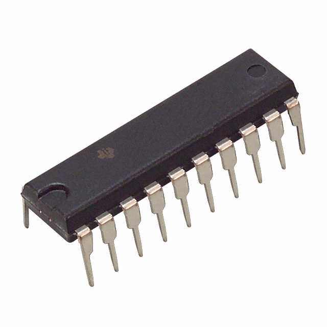
| 描述 | IC COUNTER SYNCH 4BIT U/D 20-DIP计数器 IC 4bit Synch Up/Dn |
| 产品分类 | |
| 品牌 | Texas Instruments |
| 产品手册 | |
| 产品图片 |
|
| rohs | 符合RoHS无铅 / 符合限制有害物质指令(RoHS)规范要求 |
| 产品系列 | 计数器 IC,Texas Instruments SN74ALS569AN74ALS |
| 数据手册 | |
| 产品型号 | SN74ALS569AN |
| PCN设计/规格 | |
| 产品种类 | 计数器 IC |
| 位数 | 4 bit |
| 供应商器件封装 | 20-PDIP |
| 元件数 | 1 |
| 其它名称 | 296-33750-5 |
| 包装 | 管件 |
| 单位重量 | 1.199 g |
| 商标 | Texas Instruments |
| 复位 | 异步/同步 |
| 安装类型 | 通孔 |
| 安装风格 | Through Hole |
| 定时 | 同步 |
| 封装 | Tube |
| 封装/外壳 | 20-DIP(0.300",7.62mm) |
| 封装/箱体 | PDIP-20 |
| 工作温度 | 0°C ~ 70°C |
| 工作温度范围 | 0 C to + 70 C |
| 工作电源电压 | 4.5 V to 5.5 V |
| 工厂包装数量 | 20 |
| 方向 | 上,下 |
| 标准包装 | 20 |
| 每元件位数 | 4 |
| 电压-电源 | 4.5 V ~ 5.5 V |
| 系列 | SN74ALS569A |
| 触发器类型 | 正边沿 |
| 计数器类型 | Binary |
| 计数速率 | 30MHz |
| 计数顺序 | Up/Down |
| 逻辑类型 | 二进制计数器 |
| 逻辑系列 | TTL |


PDF Datasheet 数据手册内容提取
SN54ALS569A, SN74ALS568A, SN74ALS569A SYNCHRONOUS 4-BIT UP/DOWN DECADE AND BINARY COUNTERS WITH 3-STATE OUTPUTS SDAS229A – APRIL 1982 – REVISED JANUARY 1995 • 3-State Q Outputs Drive Bus Lines Directly SN54ALS569A...J PACKAGE • SN74ALS568A, SN74ALS569A...DW OR N PACKAGE Counter Operation Independent of 3-State (TOP VIEW) Output • Fully Synchronous Clear, Count, and Load U/D 1 20 VCC • Asynchronous Clear Is Also Provided CLK 2 19 RCO • Fully Cascadable A 3 18 CCO • B 4 17 OE Package Options Include Plastic Small-Outline (DW) Packages, Ceramic C 5 16 QA Chip Carriers (FK), and Standard Plastic (N) D 6 15 QB and Ceramic (J) 300-mil DIPs ENP 7 14 QC ACLR 8 13 QD description SCLR 9 12 ENT GND 10 11 LOAD The SN74ALS568A decade counter and ′ALS569A binary counters are programmable, SN54ALS569A...FK PACKAGE count up or down, and offer both synchronous and (TOP VIEW) asynchronous clearing. All synchronous functions aclroec ke x(CecLuKte) din pount .the positive-going edge of the ACLK U/DVCCRCO The clear function is initiated by applying a low 3 2 1 20 19 level to either asynchronous clear (ACLR) or B 4 18 CCO synchronous clear (SCLR). Asynchronous (direct) C 5 17 OE clearing overrides all other functions of the device, D 6 16 QA while synchronous clearing overrides only the ENP 7 15 QB other synchronous functions. Data is loaded from ACLR 8 14 QC 9 10 1112 13 the A, B, C, and D inputs by holding load (LOAD) low during a positive-going clock transition. The R D D T D L N A NQ counting function is enabled only when enable P C G O E S L (ENP) and enable T (ENT) are low and ACLR, SCLR, and LOAD are high. The up/down (U/D) input controls the direction of the count. These counters count up when U/D is high and count down when U/D is low. A high level at the output-enable (OE) input forces the Q outputs into the high-impedance state, and a low level enables those outputs. Counting is independent of OE. ENT is fed forward to enable the ripple-carry output (RCO) to produce a low-level pulse while the count is zero (all Q outputs low) when counting down or maximum (9 or 15) when counting up. The clocked carry output (CCO) produces a low-level pulse for a duration equal to that of the low level of the clock when RCO is low and the counter is enabled (both ENP and ENT are low); otherwise, CCO is high. CCO does not have the glitches commonly associated with a ripple-carry output. Cascading is normally accomplished by connecting RCO or CCO of the first counter to ENT of the next counter. However, for very high-speed counting, RCO should be used for cascading since CCO does not become active until the clock returns to the low level. The SN54ALS569A is characterized for operation over the full military temperature range of –55°C to 125°C. The SN74ALS568A and SN74ALS569A are characterized for operation from 0°C to 70°C. PRODUCTION DATA information is current as of publication date. Copyright 1995, Texas Instruments Incorporated Products conform to specifications per the terms of Texas Instruments standard warranty. Production processing does not necessarily include testing of all parameters. POST OFFICE BOX 655303 • DALLAS, TEXAS 75265 1
SN54ALS569A, SN74ALS568A, SN74ALS569A SYNCHRONOUS 4-BIT UP/DOWN DECADE AND BINARY COUNTERS WITH 3-STATE OUTPUTS SDAS229A – APRIL 1982 – REVISED JANUARY 1995 FUNCTION TABLE INPUTS OOPPEERRAATTIIOONN OE ACLR SCLR LOAD ENT ENP U/D CLK H X X X X X X X Q outputs disabled L L X X X X X X Asynchronous clear L H L X X X X ↑ Synchronous clear L H H L X X X ↑ Load L H H H L L H ↑ Count up L H H H L L L ↑ Count down L H H H H X X X Inhibit count L H H H X H X X Inhibit count 2 POST OFFICE BOX 655303 • DALLAS, TEXAS 75265
SN54ALS569A, SN74ALS568A, SN74ALS569A SYNCHRONOUS 4-BIT UP/DOWN DECADE AND BINARY COUNTERS WITH 3-STATE OUTPUTS SDAS229A – APRIL 1982 – REVISED JANUARY 1995 logic symbols† SN74ALS568A 17 CTRDIV10 OE EN10 1 U/D M1 [UP] M2 [DOWN] 2 CLK C5/1,4,7,8,+/2,4,7,8– 18 Z6 6,7,8,9 CCO 12 19 ENT G7 1,7 (CT=9) G9 RCO 7 ENP G8 2,7 (CT=0) G9 9 SCLR 5CT=0 11 LOAD M3 [LOAD] M4 [COUNT] 8 ACLR CT=0 3 16 A 3,5D 10 QA 4 15 B QB 5 14 C QC 6 13 D QD ′ALS569A 17 CTRDIV16 OE EN10 1 U/D M1 [UP] M2 [DOWN] 2 CLK C5/1,4,7,8,+/2,4,7,8– 18 Z6 6,7,8,9 CCO 12 19 ENT G7 1,7 (CT=15) G9 RCO 7 ENP G8 2,7 (CT=0) G9 9 SCLR 5CT=0 11 LOAD M3 [LOAD] M4 [COUNT] 8 ACLR CT=0 3 16 A 3,5D 10 QA 4 15 B QB 5 14 C QC 6 13 D QD †These symbols are in accordance with ANSI/IEEE Std 91-1984 and IEC Publication 617-12. POST OFFICE BOX 655303 • DALLAS, TEXAS 75265 3
SN54ALS569A, SN74ALS568A, SN74ALS569A SYNCHRONOUS 4-BIT UP/DOWN DECADE AND BINARY COUNTERS WITH 3-STATE OUTPUTS SDAS229A – APRIL 1982 – REVISED JANUARY 1995 logic diagrams (positive logic) SN74ALS568A 17 OE 1 U/D 2 CLK 12 ENT 18 CCO 7 ENP 19 RCO 9 SCLR 11 LOAD 8 ACLR 3 A C1 1D 16 R QA 4 B C1 1D 15 R QB 5 C C1 1D 14 R QC 6 D C1 1D 13 R QD 4 POST OFFICE BOX 655303 • DALLAS, TEXAS 75265
SN54ALS569A, SN74ALS568A, SN74ALS569A SYNCHRONOUS 4-BIT UP/DOWN DECADE AND BINARY COUNTERS WITH 3-STATE OUTPUTS SDAS229A – APRIL 1982 – REVISED JANUARY 1995 logic diagrams (positive logic) (continued) ′ALS569A 17 OE 1 U/D 2 CLK 12 ENT 18 CCO 7 ENP 19 RCO 9 SCLR 11 LOAD 8 ACLR 3 A C1 1D 16 R QA 4 B C1 1D 15 R QB 5 C C1 1D 14 R QC 6 D C1 1D 13 R QD POST OFFICE BOX 655303 • DALLAS, TEXAS 75265 5
SN54ALS569A, SN74ALS568A, SN74ALS569A SYNCHRONOUS 4-BIT UP/DOWN DECADE AND BINARY COUNTERS WITH 3-STATE OUTPUTS SDAS229A – APRIL 1982 – REVISED JANUARY 1995 typical load, count, and inhibit sequences SN74ALS568A OE ACLR ÌÌ SCLRÌÌ ÌÌ LOAD ÌÌÌÌ ÌÌÌÌ ENPÌÌ ÌDÌon’tÌ CareÌ ÌÌ ÌÌÌÌ ENT Don’t Care ÌÌÌÌ ÌÌÌÌ ÌÌÌÌÌÌ U/DÌÌ ÌÌDÌon’t ÌCareÌÌ CLK ÌÌÌÌÌÌÌÌÌÌÌÌÌÌÌÌÌÌÌÌÌÌÌÌÌÌÌÌÌ AÌÌDÌon’t ÌCareÌÌÌÌÌÌÌÌÌÌÌÌÌDonÌ’t CaÌre ÌÌÌÌÌÌÌÌÌÌ BÌÌDÌon’t ÌCareÌÌÌÌÌÌÌÌÌÌÌÌÌDonÌ’t CaÌre ÌÌÌÌÌÌÌÌÌÌ ÌÌÌÌÌÌÌÌÌÌÌÌÌÌÌÌÌÌÌÌÌÌÌÌÌÌÌÌÌ C Don’t Care Don’t Care ÌÌÌÌÌÌÌÌÌÌÌÌÌÌÌÌÌÌÌÌÌÌÌÌÌÌÌÌÌÌÌÌÌÌÌÌÌÌÌÌÌÌÌÌÌÌÌÌÌÌÌÌÌÌÌÌÌÌ DÌÌDÌon’t ÌCareÌÌÌÌÌÌÌÌÌÌÌÌÌDonÌ’t CaÌre ÌÌÌÌÌÌÌÌÌÌ ÌÌÌÌ QA Hi Z ÌÌÌÌÌÌÌÌ QB ÌÌHiÌ Z Ì ÌÌÌÌ QC Hi Z ÌÌÌÌ QD ÌÌHiÌ Z Ì RCO CCO 1 2 0 7 8 9 0 1 2 3 4 3 2 1 0 9 8 Count Up Inhibit Count Up Count Down Counting Async Sync Sync Clear Clear Load 6 POST OFFICE BOX 655303 • DALLAS, TEXAS 75265
SN54ALS569A, SN74ALS568A, SN74ALS569A SYNCHRONOUS 4-BIT UP/DOWN DECADE AND BINARY COUNTERS WITH 3-STATE OUTPUTS SDAS229A – APRIL 1982 – REVISED JANUARY 1995 typical load, count, and inhibit sequences (continued) ′ALS569A OE ACLR ÌÌ SCLRÌÌ ÌÌ LOAD ÌÌÌÌ ÌÌÌÌ ENPÌÌ ÌDÌon’tÌ CareÌ ÌÌ ÌÌÌÌ ENT Don’t Care ÌÌÌÌ ÌÌÌÌ ÌÌÌÌÌÌ U/DÌÌ ÌÌDÌon’t ÌCareÌÌ CLK ÌÌÌÌÌÌÌÌÌÌÌÌÌÌÌÌÌÌÌÌÌÌÌÌÌÌÌÌÌ AÌÌDÌon’t ÌCareÌÌÌÌÌÌÌÌÌÌÌÌÌDonÌ’t CaÌre ÌÌÌÌÌÌÌÌÌÌ BÌÌDÌon’t ÌCareÌÌÌÌÌÌÌÌÌÌÌÌÌDonÌ’t CaÌre ÌÌÌÌÌÌÌÌÌÌ ÌÌÌÌÌÌÌÌÌÌÌÌÌÌÌÌÌÌÌÌÌÌÌÌÌÌÌÌÌ C Don’t Care Don’t Care ÌÌÌÌÌÌÌÌÌÌÌÌÌÌÌÌÌÌÌÌÌÌÌÌÌÌÌÌÌÌÌÌÌÌÌÌÌÌÌÌÌÌÌÌÌÌÌÌÌÌÌÌÌÌÌÌÌÌ DÌÌDÌon’t ÌCareÌÌÌÌÌÌÌÌÌÌÌÌÌDonÌ’t CaÌre ÌÌÌÌÌÌÌÌÌÌ ÌÌÌÌ QA Hi Z ÌÌÌÌÌÌÌÌ QB ÌÌHiÌ Z Ì ÌÌÌÌ QC Hi Z ÌÌÌÌ QD ÌÌHiÌ Z Ì RCO CCO 1 2 0 13 14 15 0 1 2 3 4 3 2 1 0 15 14 Count Up Inhibit Count Up Count Down Counting Async Sync Sync Clear Clear Load POST OFFICE BOX 655303 • DALLAS, TEXAS 75265 7
SN54ALS569A, SN74ALS568A, SN74ALS569A SYNCHRONOUS 4-BIT UP/DOWN DECADE AND BINARY COUNTERS WITH 3-STATE OUTPUTS SDAS229A – APRIL 1982 – REVISED JANUARY 1995 absolute maximum ratings over operating free-air temperature range (unless otherwise noted)† Supply voltage, V . . . . . . . . . . . . . . . . . . . . . . . . . . . . . . . . . . . . . . . . . . . . . . . . . . . . . . . . . . . . . . . . . . . . . . . . 7 V CC Input voltage, V . . . . . . . . . . . . . . . . . . . . . . . . . . . . . . . . . . . . . . . . . . . . . . . . . . . . . . . . . . . . . . . . . . . . . . . . . . . . 7 V I Voltage applied to a disabled 3-state output . . . . . . . . . . . . . . . . . . . . . . . . . . . . . . . . . . . . . . . . . . . . . . . . . . 5.5 V Operating free-air temperature range, T : SN54ALS569A . . . . . . . . . . . . . . . . . . . . . . . . . . . –55°C to 125°C A SN74ALS568A, SN74ALS569A . . . . . . . . . . . . . . . . . 0°C to 70°C Storage temperature range . . . . . . . . . . . . . . . . . . . . . . . . . . . . . . . . . . . . . . . . . . . . . . . . . . . . . . . –65°C to 150°C †Stresses beyond those listed under “absolute maximum ratings” may cause permanent damage to the device. These are stress ratings only, and functional operation of the device at these or any other conditions beyond those indicated under “recommended operating conditions” is not implied. Exposure to absolute-maximum-rated conditions for extended periods may affect device reliability. recommended operating conditions SN74ALS568A SN54ALS569A SN74ALS569A UNIT MIN NOM MAX MIN NOM MAX VCC Supply voltage 4.5 5 5.5 4.5 5 5.5 V VIH High-level input voltage 2 2 V VIL Low-level input voltage 0.7 0.8 V Q outputs –1 –2.6 IIOOHH HHiigghh-lleevveell oouuttppuutt ccuurrrreenntt mmAA CCO and RCO –0.4 –0.4 Q outputs 12 24 IIOOLL LLooww-lleevveell oouuttppuutt ccuurrrreenntt mmAA CCO and RCO 4 8 SN74ALS568A 0 20 ffcllockk CClloocckk ffrreeqquueennccyy MMHHzz ′ALS569A 0 22 0 30 ACLR or LOAD low 20 15 CLK high 25 SSNN7744AALLSS556688AA tw Pulse duration CLK low 25 ns CLK high 20 16.5 ′′AALLSS556699AA CLK low 23 16.5 Data at A, B, C, D 25 20 High 35 30 EENNPP, EENNTT Low 25 20 Low 20 15 SSCCLLRR tsu Setup time before CLK↑ High (inactive) 35 30 ns Low 20 15 LLOOAADD High (inactive) 35 30 U/D 35 30 ACLR inactive 10 10 th Hold time after CLK↑ for any input 0 0 ns TA Operating free-air temperature –55 125 0 70 °C 8 POST OFFICE BOX 655303 • DALLAS, TEXAS 75265
SN54ALS569A, SN74ALS568A, SN74ALS569A SYNCHRONOUS 4-BIT UP/DOWN DECADE AND BINARY COUNTERS WITH 3-STATE OUTPUTS SDAS229A – APRIL 1982 – REVISED JANUARY 1995 electrical characteristics over recommended operating free-air temperature range (unless otherwise noted) SN74ALS568A SN54ALS569A PARAMETER TEST CONDITIONS SN74ALS569A UNIT MIN TYP† MAX MIN TYP† MAX VIK VCC = 4.5 V, II = –18 mA –1.5 –1.5 V All outputs VCC = 4.5 V to 5.5 V, IOH = –0.4 mA VCC –2 VCC –2 VOH IOH = –1 mA 2.4 3.3 V QQ oouuttppuuttss VVCCCC == 44.55 VV IOH = –2.6 mA 2.4 3.2 IOL = 12 mA 0.25 0.4 0.25 0.4 QQ oouuttppuuttss VVCCCC == 44.55 VV IOL = 24 mA 0.35 0.5 VVOOLL VV IOL = 4 mA 0.25 0.4 0.25 0.4 CCCCOO aanndd RRCCOO VVCCCC == 44.55 VV IOL = 8 mA 0.35 0.5 IOZH VCC = 5.5 V, VO = 2.7 V 20 20 m A IOZL VCC = 5.5 V, VO = 0.4 V –20 –20 m A II VCC = 5.5 V, VI = 7 V 0.1 0.1 mA IIH VCC = 5.5 V, VI = 2.7 V 20 20 m A IIL VCC = 5.5 V, VI = 0.4 V –0.2 –0.2 mA CCO and RCO –15 –70 –15 –70 IIOO‡‡ VVCCCC == 55.55 VV, VVOO == 22.2255 VV mmAA Q outputs –20 –112 –30 –112 Outputs high 16 26 16 26 ICC VCC = 5.5 V Outputs low 20 32 20 32 mA Outputs disabled 20 32 20 32 †All typical values are at VCC = 5 V, TA = 25°C. ‡The output conditions have been chosen to produce a current that closely approximates one half of the true short-circuit output current, IOS. POST OFFICE BOX 655303 • DALLAS, TEXAS 75265 9
SN54ALS569A, SN74ALS568A, SN74ALS569A SYNCHRONOUS 4-BIT UP/DOWN DECADE AND BINARY COUNTERS WITH 3-STATE OUTPUTS SDAS229A – APRIL 1982 – REVISED JANUARY 1995 switching characteristics (see Figure 1) VCC = 4.5 V to 5.5 V, CL = 50 pF, R1 = 500 W , R2 = 500 W , FROM TO PARAMETER ((IINNPPUUTT)) ((OOUUTTPPUUTT)) TA = MIN to MAX† UNIT SN74ALS568A SN54ALS569A SN74ALS569A MIN MAX MIN MAX SN74ALS568A 20 ffmax MMHHzz ′ALS569A 22 30 tPLH 4 21 4 13 CCLLKK AAnny QQ nnss tPHL 7 19 7 16 tPLH 12 37 12 28 CCLLKK RRCCOO nnss tPHL 10 28 10 19 tPLH 5 17 5 13 CCLLKK CCCCOO nnss tPHL 6 30 6 25 tPLH 9 31 9 23 UU//DD RRCCOO nnss tPHL 9 33 9 19 tPLH 6 21 6 15 EENNTT RRCCOO nnss tPHL 4 20 4 13 tPLH 5 18 5 13 EENNTT CCCCOO nnss tPHL 9 32 9 23 tPLH 4 18 4 12 EENNPP CCCCOO nnss tPHL 5 18 5 14 tPHL ACLR Any Q 9 25 9 20 ns tPZH 6 23 6 18 OOEE AAnny QQ nnss tPZL 6 29 6 24 tPHZ 1 12 1 10 OOEE AAnnyy QQ nnss tPLZ 3 29 3 13 †For conditions shown as MIN or MAX, use the appropriate value specified under recommended operating conditions. 10 POST OFFICE BOX 655303 • DALLAS, TEXAS 75265
SN54ALS569A, SN74ALS568A, SN74ALS569A SYNCHRONOUS 4-BIT UP/DOWN DECADE AND BINARY COUNTERS WITH 3-STATE OUTPUTS SDAS229A – APRIL 1982 – REVISED JANUARY 1995 PARAMETER MEASUREMENT INFORMATION SERIES 54ALS/74ALS AND 54AS/74AS DEVICES 7 V VCC RL = R1 = R2 S1 RL R1 From Output Test From Output Test From Output Test Under Test Point Under Test Point Under Test Point (see NoteC AL) RL CL (see NoteC AL) R2 (see Note A) LOAD CIRCUIT FOR BI-STATE LOAD CIRCUIT LOAD CIRCUIT TOTEM-POLE OUTPUTS FOR OPEN-COLLECTOR OUTPUTS FOR 3-STATE OUTPUTS 3.5 V 3.5 V Timing High-Level Input 1.3 V Pulse 1.3 V 1.3 V 0.3 V 0.3 V tsu th tw 3.5 V 3.5 V Data Low-Level Input 1.3 V 1.3 V Pulse 1.3 V 1.3 V 0.3 V 0.3 V VOLTAGE WAVEFORMS VOLTAGE WAVEFORMS SETUP AND HOLD TIMES PULSE DURATIONS 3.5 V Output Control 1.3 V 1.3 V (low-level enabling) 0.3 V 3.5 V tPZL Input 1.3 V 1.3 V tPLZ (cid:1)3.5 V 0.3 V Waveform 1 tPLH tPHL S1 Closed 1.3 V In-Phase VOH (see Note B) VOL Output 1.3 V 1.3 V tPHZ 0.3 V VOL tPZH tPLH VOH tPHL Waveform 2 Out-of-Phase VOH S1 Open 1.3 V 0.3 V Output 1.3 V 1.3 V (see Note B) (cid:1)0 V (see Note C) VOL VOLTAGE WAVEFORMS VOLTAGE WAVEFORMS ENABLE AND DISABLE TIMES, 3-STATE OUTPUTS PROPAGATION DELAY TIMES NOTES: A. CL includes probe and jig capacitance. B. Waveform 1 is for an output with internal conditions such that the output is low except when disabled by the output control. Waveform 2 is for an output with internal conditions such that the output is high except when disabled by the output control. C. When measuring propagation delay items of 3-state outputs, switch S1 is open. D. All input pulses have the following characteristics: PRR ≤ 1 MHz, tr = tf = 2 ns, duty cycle = 50%. E. The outputs are measured one at a time with one transition per measurement. Figure 1. Load Circuits and Voltage Waveforms POST OFFICE BOX 655303 • DALLAS, TEXAS 75265 11
PACKAGE OPTION ADDENDUM www.ti.com 6-Feb-2020 PACKAGING INFORMATION Orderable Device Status Package Type Package Pins Package Eco Plan Lead/Ball Finish MSL Peak Temp Op Temp (°C) Device Marking Samples (1) Drawing Qty (2) (6) (3) (4/5) 83025022A ACTIVE LCCC FK 20 1 TBD POST-PLATE N / A for Pkg Type -55 to 125 83025022A SNJ54ALS 569AFK 8302502RA ACTIVE CDIP J 20 1 TBD Call TI N / A for Pkg Type -55 to 125 8302502RA SNJ54ALS569AJ SN54ALS569AJ ACTIVE CDIP J 20 1 TBD Call TI N / A for Pkg Type -55 to 125 SN54ALS569AJ SN74ALS569ADWR ACTIVE SOIC DW 20 2000 Green (RoHS NIPDAU Level-1-260C-UNLIM 0 to 70 ALS569A & no Sb/Br) SN74ALS569AN ACTIVE PDIP N 20 20 Pb-Free NIPDAU N / A for Pkg Type 0 to 70 SN74ALS569AN (RoHS) SN74ALS569ANE4 ACTIVE PDIP N 20 20 Pb-Free NIPDAU N / A for Pkg Type 0 to 70 SN74ALS569AN (RoHS) SNJ54ALS569AFK ACTIVE LCCC FK 20 1 TBD POST-PLATE N / A for Pkg Type -55 to 125 83025022A SNJ54ALS 569AFK SNJ54ALS569AJ ACTIVE CDIP J 20 1 TBD Call TI N / A for Pkg Type -55 to 125 8302502RA SNJ54ALS569AJ (1) The marketing status values are defined as follows: ACTIVE: Product device recommended for new designs. LIFEBUY: TI has announced that the device will be discontinued, and a lifetime-buy period is in effect. NRND: Not recommended for new designs. Device is in production to support existing customers, but TI does not recommend using this part in a new design. PREVIEW: Device has been announced but is not in production. Samples may or may not be available. OBSOLETE: TI has discontinued the production of the device. (2) RoHS: TI defines "RoHS" to mean semiconductor products that are compliant with the current EU RoHS requirements for all 10 RoHS substances, including the requirement that RoHS substance do not exceed 0.1% by weight in homogeneous materials. Where designed to be soldered at high temperatures, "RoHS" products are suitable for use in specified lead-free processes. TI may reference these types of products as "Pb-Free". RoHS Exempt: TI defines "RoHS Exempt" to mean products that contain lead but are compliant with EU RoHS pursuant to a specific EU RoHS exemption. Green: TI defines "Green" to mean the content of Chlorine (Cl) and Bromine (Br) based flame retardants meet JS709B low halogen requirements of <=1000ppm threshold. Antimony trioxide based flame retardants must also meet the <=1000ppm threshold requirement. (3) MSL, Peak Temp. - The Moisture Sensitivity Level rating according to the JEDEC industry standard classifications, and peak solder temperature. (4) There may be additional marking, which relates to the logo, the lot trace code information, or the environmental category on the device. Addendum-Page 1
PACKAGE OPTION ADDENDUM www.ti.com 6-Feb-2020 (5) Multiple Device Markings will be inside parentheses. Only one Device Marking contained in parentheses and separated by a "~" will appear on a device. If a line is indented then it is a continuation of the previous line and the two combined represent the entire Device Marking for that device. (6) Lead/Ball Finish - Orderable Devices may have multiple material finish options. Finish options are separated by a vertical ruled line. Lead/Ball Finish values may wrap to two lines if the finish value exceeds the maximum column width. Important Information and Disclaimer:The information provided on this page represents TI's knowledge and belief as of the date that it is provided. TI bases its knowledge and belief on information provided by third parties, and makes no representation or warranty as to the accuracy of such information. Efforts are underway to better integrate information from third parties. TI has taken and continues to take reasonable steps to provide representative and accurate information but may not have conducted destructive testing or chemical analysis on incoming materials and chemicals. TI and TI suppliers consider certain information to be proprietary, and thus CAS numbers and other limited information may not be available for release. In no event shall TI's liability arising out of such information exceed the total purchase price of the TI part(s) at issue in this document sold by TI to Customer on an annual basis. OTHER QUALIFIED VERSIONS OF SN54ALS569A, SN74ALS569A : •Catalog: SN74ALS569A •Military: SN54ALS569A NOTE: Qualified Version Definitions: •Catalog - TI's standard catalog product •Military - QML certified for Military and Defense Applications Addendum-Page 2
PACKAGE MATERIALS INFORMATION www.ti.com 14-Jul-2012 TAPE AND REEL INFORMATION *Alldimensionsarenominal Device Package Package Pins SPQ Reel Reel A0 B0 K0 P1 W Pin1 Type Drawing Diameter Width (mm) (mm) (mm) (mm) (mm) Quadrant (mm) W1(mm) SN74ALS569ADWR SOIC DW 20 2000 330.0 24.4 10.8 13.0 2.7 12.0 24.0 Q1 PackMaterials-Page1
PACKAGE MATERIALS INFORMATION www.ti.com 14-Jul-2012 *Alldimensionsarenominal Device PackageType PackageDrawing Pins SPQ Length(mm) Width(mm) Height(mm) SN74ALS569ADWR SOIC DW 20 2000 367.0 367.0 45.0 PackMaterials-Page2
None
None
PACKAGE OUTLINE DW0020A SOIC - 2.65 mm max height SCALE 1.200 SOIC C 10.63 SEATING PLANE TYP 9.97 A PIN 1 ID 0.1 C AREA 18X 1.27 20 1 13.0 2X 12.6 11.43 NOTE 3 10 11 0.51 20X 7.6 0.31 2.65 MAX B 7.4 0.25 C A B NOTE 4 0.33 TYP 0.10 0.25 SEE DETAIL A GAGE PLANE 0.3 1.27 0 - 8 0.1 0.40 DETAIL A TYPICAL 4220724/A 05/2016 NOTES: 1. All linear dimensions are in millimeters. Dimensions in parenthesis are for reference only. Dimensioning and tolerancing per ASME Y14.5M. 2. This drawing is subject to change without notice. 3. This dimension does not include mold flash, protrusions, or gate burrs. Mold flash, protrusions, or gate burrs shall not exceed 0.15 mm per side. 4. This dimension does not include interlead flash. Interlead flash shall not exceed 0.43 mm per side. 5. Reference JEDEC registration MS-013. www.ti.com
EXAMPLE BOARD LAYOUT DW0020A SOIC - 2.65 mm max height SOIC 20X (2) SYMM 1 20 20X (0.6) 18X (1.27) SYMM (R0.05) TYP 10 11 (9.3) LAND PATTERN EXAMPLE SCALE:6X SOOPLEDNEINRG MASK METAL MSOELTDAEL RU NMDAESRK SOOPLEDNEINRG MASK 0.07 MAX 0.07 MIN ALL AROUND ALL AROUND NON SOLDER MASK SOLDER MASK DEFINED DEFINED SOLDER MASK DETAILS 4220724/A 05/2016 NOTES: (continued) 6. Publication IPC-7351 may have alternate designs. 7. Solder mask tolerances between and around signal pads can vary based on board fabrication site. www.ti.com
EXAMPLE STENCIL DESIGN DW0020A SOIC - 2.65 mm max height SOIC 20X (2) SYMM 1 20 20X (0.6) 18X (1.27) SYMM 10 11 (9.3) SOLDER PASTE EXAMPLE BASED ON 0.125 mm THICK STENCIL SCALE:6X 4220724/A 05/2016 NOTES: (continued) 8. Laser cutting apertures with trapezoidal walls and rounded corners may offer better paste release. IPC-7525 may have alternate design recommendations. 9. Board assembly site may have different recommendations for stencil design. www.ti.com
None
IMPORTANTNOTICEANDDISCLAIMER TI PROVIDES TECHNICAL AND RELIABILITY DATA (INCLUDING DATASHEETS), DESIGN RESOURCES (INCLUDING REFERENCE DESIGNS), APPLICATION OR OTHER DESIGN ADVICE, WEB TOOLS, SAFETY INFORMATION, AND OTHER RESOURCES “AS IS” AND WITH ALL FAULTS, AND DISCLAIMS ALL WARRANTIES, EXPRESS AND IMPLIED, INCLUDING WITHOUT LIMITATION ANY IMPLIED WARRANTIES OF MERCHANTABILITY, FITNESS FOR A PARTICULAR PURPOSE OR NON-INFRINGEMENT OF THIRD PARTY INTELLECTUAL PROPERTY RIGHTS. These resources are intended for skilled developers designing with TI products. You are solely responsible for (1) selecting the appropriate TI products for your application, (2) designing, validating and testing your application, and (3) ensuring your application meets applicable standards, and any other safety, security, or other requirements. These resources are subject to change without notice. TI grants you permission to use these resources only for development of an application that uses the TI products described in the resource. Other reproduction and display of these resources is prohibited. No license is granted to any other TI intellectual property right or to any third party intellectual property right. TI disclaims responsibility for, and you will fully indemnify TI and its representatives against, any claims, damages, costs, losses, and liabilities arising out of your use of these resources. TI’s products are provided subject to TI’s Terms of Sale (www.ti.com/legal/termsofsale.html) or other applicable terms available either on ti.com or provided in conjunction with such TI products. TI’s provision of these resources does not expand or otherwise alter TI’s applicable warranties or warranty disclaimers for TI products. Mailing Address: Texas Instruments, Post Office Box 655303, Dallas, Texas 75265 Copyright © 2020, Texas Instruments Incorporated