
 Datasheet下载
- 型号: SN74AHCT16373DGVR
- 制造商: Texas Instruments
- 库位|库存: xxxx|xxxx
- 要求:
| 数量阶梯 | 香港交货 | 国内含税 |
| +xxxx | $xxxx | ¥xxxx |
查看当月历史价格
查看今年历史价格
SN74AHCT16373DGVR产品简介:
ICGOO电子元器件商城为您提供SN74AHCT16373DGVR由Texas Instruments设计生产,在icgoo商城现货销售,并且可以通过原厂、代理商等渠道进行代购。 SN74AHCT16373DGVR价格参考。Texas InstrumentsSN74AHCT16373DGVR封装/规格:逻辑 - 锁销, D-Type Transparent Latch 2 Channel 8:8 IC Tri-State 48-TVSOP。您可以下载SN74AHCT16373DGVR参考资料、Datasheet数据手册功能说明书,资料中有SN74AHCT16373DGVR 详细功能的应用电路图电压和使用方法及教程。
SN74AHCT16373DGVR 是 Texas Instruments(德州仪器)生产的一款 16 位透明 D 类锁存器,属于逻辑 - 锁销类器件。该芯片广泛应用于需要并行数据存储与传输的数字电路系统中。

其主要应用场景包括:

1. 数据缓冲与存储:用于临时存储 16 位并行数据,适用于数据总线隔离、数据暂存等场合。
2. 地址锁存:在微处理器或存储器接口设计中,用于锁存地址信号,以实现对外部设备或存储单元的选择控制。
3. 工业控制系统:如PLC(可编程逻辑控制器)、自动化设备中,用于控制信号的同步和保持。
4. 通信设备:用于数据总线管理、信号转换及接口扩展,提高系统的稳定性和抗干扰能力。
5. 测试测量仪器:在示波器、逻辑分析仪等设备中用于数据采集与处理。

该器件具有低功耗、高速CMOS工艺、宽工作温度范围(工业级-40℃~85℃),适合工业环境应用。TSSOP封装(DGVR)便于PCB布局,适用于高密度电路设计。
| 参数 | 数值 |
| 产品目录 | 集成电路 (IC) |
| 描述 | IC 16BIT TRANSP D LATCH 48-TVSOP |
| 产品分类 | |
| 品牌 | Texas Instruments |
| 数据手册 | |
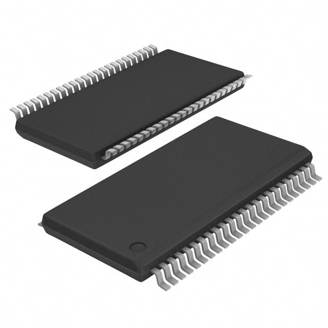
| 产品图片 |
|
| 产品型号 | SN74AHCT16373DGVR |
| rohs | 无铅 / 符合限制有害物质指令(RoHS)规范要求 |
| 产品系列 | 74AHCT |
| 供应商器件封装 | 48-TVSOP |
| 其它名称 | 296-4691-6 |
| 包装 | Digi-Reel® |
| 安装类型 | 表面贴装 |
| 封装/外壳 | 48-TFSOP(0.173",4.40mm 宽) |
| 工作温度 | -40°C ~ 85°C |
| 延迟时间-传播 | 1ns |
| 标准包装 | 1 |
| 独立电路 | 2 |
| 电压-电源 | 4.5 V ~ 5.5 V |
| 电流-输出高,低 | 8mA,8mA |
| 电路 | 8:8 |
| 输出类型 | 三态 |
| 逻辑类型 | D 型透明锁存器 |


PDF Datasheet 数据手册内容提取
Product Sample & Technical Tools & Support & Folder Buy Documents Software Community SN54AHCT16373,SN74AHCT16373 SCLS336I–JANUARY2000–REVISEDAUGUST2014 SNx4AHCT16373 16-Bit Transparent D-Type Latches With 3-State Outputs 1 Features 2 Applications • MembersoftheTexasInstrumentsWidebus™ • WearableHealthandFitnessDevices 1 Family • Toys • EPIC™(Enhanced-PerformanceImplanted • PCsandNotebooks CMOS)Process • PowerInfrastructures • InputsareTTL-VoltageCompatible • Servers • DistributedV andGNDPinsMinimizeHigh- CC SpeedSwitchingNoise 3 Description • Flow-ThroughArchitectureOptimizesPCBLayout The SNxAHCT16373 devices are 16-bit transparent • Latch-UpPerformanceExceeds250mAPer D-type latches with 3-state outputs designed specifically for driving highly capacitive or relatively JESD17 low-impedance loads. They are particularly suitable • ESDProtectionExceeds2000VPerMIL-STD- for implementing buffer registers, I/O ports, 883,Method3015;Exceeds200VUsingMachine bidirectionalbusdrivers,andworkingregisters. Model(C=200pF,R=0) • PackageOptionsInclude: DeviceInformation(1) – PlasticShrinkSmall-Outline(DL)Package PARTNUMBER PACKAGE BODYSIZE(NOM) – ThinShrinkSmall-Outline(DGG)Package TSSOP(48) 12.50mm×6.10mm – ThinVerySmall-Outline(DGV)Package SNx4AHC16373 TVSOP(48) 9.70mm×4.40mm SSOP(48) 15.88mm×7.49mm – 80-milFine-PitchCeramicFlat(WD)Package Using25-milCenter-to-CenterSpacings (1) For all available packages, see the orderable addendum at theendofthedatasheet. 4 Simplified Schematic 1OE 2OE 1LE 2LE C1 C1 1Q1 2Q1 1D1 1D 2D1 1D ToSevenOtherChannels ToSevenOtherChannels 1 An IMPORTANT NOTICE at the end of this data sheet addresses availability, warranty, changes, use in safety-critical applications, intellectualpropertymattersandotherimportantdisclaimers.UNLESSOTHERWISENOTED,thisdocumentcontainsPRODUCTION DATA.
SN54AHCT16373,SN74AHCT16373 SCLS336I–JANUARY2000–REVISEDAUGUST2014 www.ti.com Table of Contents 1 Features.................................................................. 1 9 DetailedDescription............................................ 10 2 Applications........................................................... 1 9.1 Overview.................................................................10 3 Description............................................................. 1 9.2 FunctionalBlockDiagrams.....................................10 4 SimplifiedSchematic............................................. 1 9.3 FeatureDescription.................................................11 9.4 DeviceFunctionalModes........................................11 5 RevisionHistory..................................................... 2 10 ApplicationandImplementation........................ 12 6 PinConfigurationandFunctions......................... 3 10.1 ApplicationInformation..........................................12 7 Specifications......................................................... 5 10.2 TypicalApplication ...............................................12 7.1 AbsoluteMaximumRatings......................................5 11 PowerSupplyRecommendations..................... 13 7.2 HandlingRatings.......................................................5 12 Layout................................................................... 13 7.3 RecommendedOperatingConditions.......................5 7.4 ThermalInformation..................................................6 12.1 LayoutGuidelines.................................................13 7.5 ElectricalCharacteristics...........................................6 12.2 LayoutExample....................................................13 7.6 TimingRequirements................................................6 13 DeviceandDocumentationSupport................. 14 7.7 SwitchingCharacteristics..........................................7 13.1 RelatedLinks........................................................14 7.8 NoiseCharacteristics................................................7 13.2 Trademarks...........................................................14 7.9 OperatingCharacteristics..........................................7 13.3 ElectrostaticDischargeCaution............................14 7.10 TypicalCharacteristics............................................8 13.4 Glossary................................................................14 8 ParameterMeasurementInformation..................9 14 Mechanical,Packaging,andOrderable Information........................................................... 14 5 Revision History NOTE:Pagenumbersforpreviousrevisionsmaydifferfrompagenumbersinthecurrentversion. ChangesfromRevisionH(January2000)toRevisionI Page • UpdateddocumenttonewTIdatasheetformat.................................................................................................................... 1 • DeletedOrderingInformationtable........................................................................................................................................ 1 • AddedApplications................................................................................................................................................................. 1 • AddedPinFunctionstable...................................................................................................................................................... 3 • AddedHandlingRatingstable................................................................................................................................................ 5 • ChangedMAXoperatingtemperatureto125°CinRecommendedOperatingConditionstable. ......................................... 5 • AddedThermalInformationtable........................................................................................................................................... 6 • Added–40°Cto125°CforSN74AHCT16373inElectricalCharacteristicstable................................................................... 6 • AddedT =–40°Cto125°CforSN74AHCT16373intheTimingRequirementstable.......................................................... 6 A • AddedT =–40°Cto125°CforSN74AHCT16373intheSwitchingCharacteristicstable.................................................... 7 A • AddedTypicalCharacteristics................................................................................................................................................ 8 • AddedDetailedDescriptionsection...................................................................................................................................... 10 • AddedApplicationandImplementationsection.................................................................................................................... 12 • AddedPowerSupplyRecommendationsandLayoutsections............................................................................................ 13 2 SubmitDocumentationFeedback Copyright©2000–2014,TexasInstrumentsIncorporated ProductFolderLinks:SN54AHCT16373 SN74AHCT16373
SN54AHCT16373,SN74AHCT16373 www.ti.com SCLS336I–JANUARY2000–REVISEDAUGUST2014 6 Pin Configuration and Functions SN54AHCT16373...WDPACKAGE SN74AHCT16373...DGG,DGV,ORDLPACKAGE (TOPVIEW) 1OE 1 48 1LE 1Q1 2 47 1D1 1Q2 3 46 1D2 GND 4 45 GND 1Q3 5 44 1D3 1Q4 6 43 1D4 VCC 7 42 VCC 1Q5 8 41 1D5 1Q6 9 40 1D6 GND 10 39 GND 1Q7 11 38 1D7 1Q8 12 37 1D8 2Q1 13 36 2D1 2Q2 14 35 2D2 GND 15 34 GND 2Q3 16 33 2D3 2Q4 17 32 2D4 VCC 18 31 VCC 2Q5 19 30 2D5 2Q6 20 29 2D6 GND 21 28 GND 2Q7 22 27 2D7 2Q8 23 26 2D8 2OE 24 25 2LE PinFunctions PIN I/O DESCRIPTION NO. NAME 1 1OE I OutputEnable1 2 1Q1 O 1Q1Output 3 1Q2 O 1Q2Output 4 GND — GroundPin 5 1Q3 O 1Q3Output 6 1Q4 O 1Q4Output 7 V — PowerPin CC 8 1Q5 O 1Q5Output 9 1Q6 O 1Q6Output 10 GND — GroundPin 11 1Q7 O 1Q7Output 12 1Q8 O 1Q8Output 13 2Q1 O 2Q1Output 14 2Q2 O 2Q2Output 15 GND — GroundPin 16 2Q3 O 2Q3Output 17 2Q4 O 2Q4Output 18 V — PowerPin CC Copyright©2000–2014,TexasInstrumentsIncorporated SubmitDocumentationFeedback 3 ProductFolderLinks:SN54AHCT16373 SN74AHCT16373
SN54AHCT16373,SN74AHCT16373 SCLS336I–JANUARY2000–REVISEDAUGUST2014 www.ti.com PinFunctions(continued) PIN I/O DESCRIPTION NO. NAME 19 2Q5 O 2Q5Output 20 2Q6 O 2Q6Output 21 GND — GroundPin 22 2Q7 O 2Q7Output 23 2Q8 O 2Q8Output 24 2OE I OutputEnable2 25 2LE I LatchEnable2 26 2D8 I 2D8Input 27 2D7 I 2D7Input 28 GND — GroundPin 29 2D6 I 2D6Input 30 2D5 I 2D5Input 31 V — PowerPin CC 32 2D4 I 2D4Input 33 2D3 I 2D3Input 34 GND — GroundPin 35 2D2 I 2D2Input 36 2D1 I 2D1Input 37 1D8 I 1D8Input 38 1D7 I 1D7Input 39 GND — GroundPin 40 1D6 I 1D6Input 41 1D5 I 1D5Input 42 V — PowerPin CC 43 1D4 I 1D4Input 44 1D3 I 1D3Input 45 GND — GroundPin 46 1D2 I 1D2Input 47 1D1 I 1D1Input 48 1LE I LatchEnable1 4 SubmitDocumentationFeedback Copyright©2000–2014,TexasInstrumentsIncorporated ProductFolderLinks:SN54AHCT16373 SN74AHCT16373
SN54AHCT16373,SN74AHCT16373 www.ti.com SCLS336I–JANUARY2000–REVISEDAUGUST2014 7 Specifications 7.1 Absolute Maximum Ratings(1) overoperatingfree-airtemperaturerange(unlessotherwisenoted) MIN MAX UNIT V Supplyvoltagerange –0.5 7 V CC V Inputvoltagerange(2) –0.5 7 V I V Outputvoltagerange(2) –0.5 V +0.5 V O CC I Inputclampcurrent V <0 –20 mA IK I I Outputclampcurrent V <0orV >V ±20 mA OK O O CC I Continuousoutputcurrent V =0toV ±25 mA O O CC ContinuouscurrentthroughV orGND ±75 mA CC (1) StressesbeyondthoselistedunderAbsoluteMaximumRatingsmaycausepermanentdamagetothedevice.Thesearestressratings only,andfunctionaloperationofthedeviceattheseoranyotherconditionsbeyondthoseindicatedunderRecommendedOperating Conditionsisnotimplied.Exposuretoabsolute-maximum-ratedconditionsforextendedperiodsmayaffectdevicereliability. (2) Theinputandoutputvoltageratingsmaybeexceedediftheinputandoutputcurrentratingsareobserved. 7.2 Handling Ratings MIN MAX UNIT T Storagetemperaturerange –65 150 °C stg Humanbodymodel(HBM),perANSI/ESDA/JEDECJS-001,all pins(1) 0 2000 V Electrostaticdischarge V (ESD) Chargeddevicemodel(CDM),perJEDECspecification JESD22-C101,allpins(2) 0 1000 (1) JEDECdocumentJEP155statesthat500-VHBMallowssafemanufacturingwithastandardESDcontrolprocess. (2) JEDECdocumentJEP157statesthat250-VCDMallowssafemanufacturingwithastandardESDcontrolprocess. 7.3 Recommended Operating Conditions overoperatingfree-airtemperaturerange(unlessotherwisenoted)(1) SN54AHCT16373(2) SN74AHCT16373 UNIT MIN MAX MIN MAX V Supplyvoltage 4.5 5.5 4.5 5.5 V CC V High-levelinputvoltage 2 2 V IH V Low-levelinputvoltage 0.8 0.8 V IL V Inputvoltage 0 5.5 0 5.5 V I V Outputvoltage 0 V 0 V V O CC CC I High-leveloutputcurrent –8 –8 mA OH I Low-leveloutputcurrent 8 8 mA OL ∆t/∆v Inputtransitionriseorfallrate 20 20 ns/V T Operatingfree-airtemperature –55 125 –40 125 °C A (1) AllunusedinputsofthedevicemustbeheldatV orGNDtoensureproperdeviceoperation.RefertotheTIapplicationreport, CC ImplicationsofSloworFloatingCMOSInputs(SCBA004). (2) ProductPreview Copyright©2000–2014,TexasInstrumentsIncorporated SubmitDocumentationFeedback 5 ProductFolderLinks:SN54AHCT16373 SN74AHCT16373
SN54AHCT16373,SN74AHCT16373 SCLS336I–JANUARY2000–REVISEDAUGUST2014 www.ti.com 7.4 Thermal Information SN74AHCT16373 THERMALMETRIC(1) DGG DGV DL UNIT 48PINS R Junction-to-ambientthermalresistance 69.9 80.9 61.4 θJA R Junction-to-case(top)thermalresistance 24.2 32.8 31.4 θJC(top) R Junction-to-boardthermalresistance 26.9 44.0 33.2 θJB °C/W ψ Junction-to-topcharacterizationparameter 1.9 3.3 9.0 JT ψ Junction-to-boardcharacterizationparameter 36.6 43.4 32.9 JB R Junction-to-case(bottom)thermalresistance n/a n/a n/a θJC(bot) (1) Formoreinformationabouttraditionalandnewthermalmetrics,seetheICPackageThermalMetricsapplicationreport(SPRA953). 7.5 Electrical Characteristics overrecommendedoperatingfree-airtemperaturerange(unlessotherwisenoted) PARAMETER TESTCONDITIONS VCC TA=25°C SN54AHCT16373(1) SN–4704°ACHtCoT8156°3C73 S–N4704°ACHtoCT112653°C73 UNIT MIN TYP MAX MIN MAX MIN MAX MIN MAX IOH=–50µA 4.4 4.5 4.4 4.4 4.4 VOH 4.5V V IOH=–8mA 3.94 3.8 3.8 3.8 IOL=50µA 0.1 0.1 0.1 0.1 VOL 4.5V V IOL=8mA 0.36 0.44 0.44 0.44 II VI=VCCorGND 05.V5tVo ±0.1 ±1(2) ±1 ±1 µA IOZ VO=VCCorGND 5.5V ±0.25 ±2.5 ±2.5 ±2.5 µA ICC VI=VCCorGND,IO=0 5.5V 4 40 40 40 µA Oneinputat3.4V, ΔICC(3) OtherinputsatVCCor 5.5V 1.35 1.5 1.5 1.5 mA GND Ci VI=VCCorGND 5V 2.5 10 10 pF Co VO=VCCorGND 5V 4.5 pF (1) ProductPreview (2) OnproductscomplianttoMIL-PRF-38535,thisparameterisnotproductiontestedatV =0V. CC (3) ThisistheincreaseinsupplycurrentforeachinputatoneofthespecifiedTTLvoltagelevelsratherthan0VorV . CC 7.6 Timing Requirements overrecommendedoperatingfree-airtemperaturerange,V =5V±0.5V(unlessotherwisenoted)(seeFigure2) CC T =25°C SN54AHCT16373(1) SN74AHCT16373 TA=–40°Cto125°C A SN74AHCT16373 UNIT MIN MAX MIN MAX MIN MAX MIN MAX t Pulseduration,LEhigh 6.5 6.5 6.5 6.5 ns w t Setuptime,databeforeLE↓ 1.5 1.5 1.5 1.5 ns su t Holdtime,dataafterLE↓ 3.5 3.5 3.5 3.5 ns h (1) ProductPreview 6 SubmitDocumentationFeedback Copyright©2000–2014,TexasInstrumentsIncorporated ProductFolderLinks:SN54AHCT16373 SN74AHCT16373
SN54AHCT16373,SN74AHCT16373 www.ti.com SCLS336I–JANUARY2000–REVISEDAUGUST2014 7.7 Switching Characteristics overrecommendedoperatingfree-airtemperaturerange,V =5V±0.5V(unlessotherwisenoted)(seeFigure2) CC PARAMETER (OFURTOPMUT) (INTPOUT) CAPALOCIATDANCE TA=25°C SN54AHCT16373(1) SN74AHCT16373 TASN=7–44A0H°CCTto16132753°C UNIT MIN TYP MAX MIN MAX MIN MAX MIN MAX ttPPLHHL D Q CL=15pF 55..11((22)) 88..55((22)) 11((22)) 99..55((22)) 11 99..55 11 1100..55 ns ttPPLHHL LE Q CL=15pF 55((22)) 88..55((22)) 11((22)) 99..55((22)) 11 99..55 11 1100..55 ns ttPPZZHL OE Q CL=15pF 55((22)) 99..55((22)) 11((22)) 1100..55((22)) 11 1100..55 11 1111..11 ns ttPPHLZZ OE Q CL=15pF 6.86((22)) 1100..22((22)) 11((22)) 1111((22)) 11 1111 11 1111..66 ns ttPPLHHL D Q CL=50pF 55..99 99..55 11 1100..55 11 1100..55 11 1111..55 ns ttPPLHHL LE Q CL=50pF 65..49 99..55 11 1100..55 11 1100..55 11 1111..55 ns ttPPZZHL OE Q CL=50pF 66 1100..55 11 1111..55 11 1111..55 11 1122..11 ns ttPPHLZZ OE Q CL=50pF 67..88 1111..22 11 1122 11 1122 11 1122..66 ns tsk(o) CL=50pF 1(3) 1 1 ns (1) ProductPreview (2) OnproductscomplianttoMIL-PRF-38535,thisparameterisnotproductiontested. (3) OnproductscomplianttoMIL-PRF-38535,thisparameterdoesnotapply. 7.8 Noise Characteristics V =5V,C =50pF,T =25°C(1) CC L A SN74AHCT16373 PARAMETER UNIT MIN TYP MAX V Quietoutput,maximumdynamicV 0.32 0.8 V OL(P) OL V Quietoutput,minimumdynamicV –0.1 –0.8 V OL(V) OL V Quietoutput,minimumdynamicV 4.7 V OH(V) OH V High-leveldynamicinputvoltage 2 V IH(D) V Low-leveldynamicinputvoltage 0.8 V IL(D) (1) Characteristicsareforsurface-mountpackagesonly. 7.9 Operating Characteristics V =5V,T =25°C CC A PARAMETER TESTCONDITIONS TYP UNIT C Powerdissipationcapacitance Noload, f=1MHz 22 pF pd Copyright©2000–2014,TexasInstrumentsIncorporated SubmitDocumentationFeedback 7 ProductFolderLinks:SN54AHCT16373 SN74AHCT16373
SN54AHCT16373,SN74AHCT16373 SCLS336I–JANUARY2000–REVISEDAUGUST2014 www.ti.com 7.10 Typical Characteristics 7 6 5 s) 4 n D ( P 3 T 2 1 TPD in ns 0 -100 -50 0 50 100 150 Temperature (qC) D001 Figure1.TPDvsTemperature 8 SubmitDocumentationFeedback Copyright©2000–2014,TexasInstrumentsIncorporated ProductFolderLinks:SN54AHCT16373 SN74AHCT16373
SN54AHCT16373,SN74AHCT16373 www.ti.com SCLS336I–JANUARY2000–REVISEDAUGUST2014 8 Parameter Measurement Information VCC FromOutput Test FromOutput RL=1kΩ S1 Open TEST S1 UnderTest Point UnderTest GND tPLH/tPHL Open CL CL tPLZ/tPZL VCC (seeNoteA) (seeNoteA) tPHZ/tPZH GND OpenDrain VCC LOADCIRCUITFOR LOADCIRCUITFOR TOTEM-POLEOUTPUTS 3-STATEANDOPEN-DRAINOUTPUTS 3V TimingInput 1.5V tw 0V th 3V tsu 3V Input 1.5V 1.5V DataInput 1.5V 1.5V 0V 0V VOLTAGEWAVEFORMS VOLTAGEWAVEFORMS PULSEDURATION SETUPANDHOLDTIMES 3V 3V Output Input 1.5V 1.5V 1.5V 1.5V Control 0V 0V tPLH tPHL tPZL tPLZ Output VOH Waveform1 ≈VCC InO-Puhtapsuet 50%VCC 50%VCC S1atVCC 50%VCC VOL+0.3V VOL (seeNoteB) VOL tPHL tPLH tPZH tPHZ Output Out-ofO-Puhtapsuet 50%VCC 50%VCVVCOOHL (WseSae1veNaftooGtremNBD2) 50%VCC VOH–0.3VV≈0OVH VOLTAGEWAVEFORMS VOLTAGEWAVEFORMS PROPAGATIONDELAYTIMES ENABLEANDDISABLETIMES INVERTINGANDNONINVERTINGOUTPUTS LOW-ANDHIGH-LEVELENABLING NOTES: A. CLincludesprobeandjigcapacitance. B. Waveform1isforanoutputwithinternalconditionssuchthattheoutputislowexceptwhendisabledbytheoutputcontrol. Waveform2isforanoutputwithinternalconditionssuchthattheoutputishighexceptwhendisabledbytheoutputcontrol. C. Allinputpulsesaresuppliedbygeneratorshavingthefollowingcharacteristics: PRR≤1MHz,ZO=50Ω,tr≤3ns,tf≤3ns. D. Theoutputsaremeasuredoneatatimewithoneinputtransitionpermeasurement. Figure2. LoadCircuitandVoltageWaveforms Copyright©2000–2014,TexasInstrumentsIncorporated SubmitDocumentationFeedback 9 ProductFolderLinks:SN54AHCT16373 SN74AHCT16373
SN54AHCT16373,SN74AHCT16373 SCLS336I–JANUARY2000–REVISEDAUGUST2014 www.ti.com 9 Detailed Description 9.1 Overview The SNxAHCT16373 devices are 16-bit transparent D-type latches with 3-state outputs designed specifically for driving highly capacitive or relatively low-impedance loads. They are particularly suitable for implementing buffer registers,IOports,bidirectionalbusdrivers,andworkingregisters. These devices can be used as two 8-bit latches or one 16-bit latch. When the latch-enable (LE) input is high, the Q outputs follow the data (D) inputs. When LE is taken low, the Q outputs are latched at the levels set up at the Dinputs. A buffered output-enable (OE) input can be used to place the eight outputs in either a normal logic state (high or low logic levels) or the high-impedance state. In the high-impedance state, the outputs neither load nor drive the bus lines significantly. The high-impedance state and the increased drive provide the capability to drive bus lines withoutneedforinterfaceorpullupcomponents. OE does not affect internal operations of the latch. Old data can be retained or new data can be entered while theoutputsareinthehigh-impedancestate. To ensure the high-impedance state during power up or power down, OE should be tied to V through a pullup CC resistor;theminimumvalueoftheresistorisdeterminedbythecurrent-sinkingcapabilityofthedriver. 9.2 Functional Block Diagrams 1OE 2OE 1LE 2LE C1 C1 1Q1 2Q1 1D1 1D 2D1 1D ToSevenOtherChannels ToSevenOtherChannels Figure3. LogicDiagram(PositiveLogic) 10 SubmitDocumentationFeedback Copyright©2000–2014,TexasInstrumentsIncorporated ProductFolderLinks:SN54AHCT16373 SN74AHCT16373
SN54AHCT16373,SN74AHCT16373 www.ti.com SCLS336I–JANUARY2000–REVISEDAUGUST2014 Functional Block Diagrams (continued) 1OE 1EN 1LE C3 2OE 2EN 2LE C4 1D1 3D 1 1Q1 1D2 1Q2 1D3 1Q3 1D4 1Q4 1D5 1Q5 1D6 1Q6 1D7 1Q7 1D8 1Q8 2D1 4D 2 2Q1 2D2 2Q2 2D3 2Q3 2D4 2Q4 2D5 2Q5 2D6 2Q6 2D7 2Q7 2D8 2Q8 ThissymbolisinaccordancewithANSI/IEEEStd91-1984andIECPublication617-12. Figure4. LogicSymbol 9.3 Feature Description • TTLinputs – Loweredswitchingthresholdallowsuptranslationfrom3.3Vto5V • Slowedgesreduceoutputringing 9.4 Device Functional Modes Table1.FunctionTable (Each8-bitLatch) INPUTS OUTPUT OE LE D Q L H H H L H L L L L X Q 0 H X X Z Copyright©2000–2014,TexasInstrumentsIncorporated SubmitDocumentationFeedback 11 ProductFolderLinks:SN54AHCT16373 SN74AHCT16373
SN54AHCT16373,SN74AHCT16373 SCLS336I–JANUARY2000–REVISEDAUGUST2014 www.ti.com 10 Application and Implementation 10.1 Application Information The SN74AHCT16373 is a low-drive CMOS device that can be used for a multitude of bus interface type applications where output ringing is a concern. The low drive and slow edge rates will minimize overshoot and undershoot on the outputs. The input switching levels have been lowered to accommodate TTL inputs of 0.8-V V and 2-V V . This feature makes it ideal for translating up from 3.3 V to 5 V. Figure 6 shows this type of IL IH translation. 10.2 Typical Application Regulated 5 V Regulated 3.3 V OE VCC LE 1D 1Q µC or 5 V µC System Logic System Logic 8D 8Q LEDs GND Figure5. TypicalApplicationSchematic 10.2.1 DesignRequirements This device uses CMOS technology and has balanced output drive. Care should be taken to avoid bus contention because it can drive currents that would exceed maximum limits. The high drive will also create fast edgesintolightloadssoroutingandloadconditionsshouldbeconsideredtopreventringing. 10.2.2 DetailedDesignProcedure 1. Recommendedinputconditions – Risetimeandfalltimespecs:See(Δt/ΔV)intheRecommendedOperatingConditionstable. – SpecifiedHighandlowlevels:See(V andV )intheRecommendedOperatingConditions table. IH IL – Inputsareovervoltagetolerantallowingthemtogoashighas5.5VatanyvalidV CC 2. Recommendoutputconditions – Loadcurrentsshouldnotexceed25mAperoutputand75mAtotalforthepart – OutputsshouldnotbepulledaboveV CC 12 SubmitDocumentationFeedback Copyright©2000–2014,TexasInstrumentsIncorporated ProductFolderLinks:SN54AHCT16373 SN74AHCT16373
SN54AHCT16373,SN74AHCT16373 www.ti.com SCLS336I–JANUARY2000–REVISEDAUGUST2014 Typical Application (continued) 10.2.3 ApplicationCurves Figure6.UpTranslation 11 Power Supply Recommendations The power supply can be any voltage between the MIN and MAX supply voltage rating located in the RecommendedOperatingConditionstable. Each V pin should have a good bypass capacitor to prevent power disturbance. For devices with a single CC supply, 0.1 μF is recommended. If there are multiple V pins, 0.01 μF or 0.022 μF is recommended for each CC powerpin.Itisacceptabletoparallelmultiplebypasscapstorejectdifferentfrequenciesofnoise.A0.1 μFand1 μF are commonly used in parallel. The bypass capacitor should be installed as close to the power pin as possibleforbestresults. 12 Layout 12.1 Layout Guidelines Whenusingmultiplebitlogicdevicesinputsshouldnoteverfloat. In many cases, functions or parts of functions of digital logic devices are unused, for example, when only two inputs of a triple-input-AND gate are used or only 3 of the 4 buffer gates are used. Such input pins should not be left unconnected because the undefined voltages at the outside connections result in undefined operational states. Specified in Figure 7 are the rules that must be observed under all circumstances. All unused inputs of digital logic devices must be connected to a high or low bias to prevent them from floating. The logic level that should be applied to any particular unused input depends on the function of the device. Generally they will be tied to GND or V ; whichever makes more sense or is more convenient. It is generally acceptable to float CC outputsunlessthepartisatransceiver. 12.2 Layout Example V cc Input Unused Input Output Unused Input Output Input Figure7. LayoutDiagram Copyright©2000–2014,TexasInstrumentsIncorporated SubmitDocumentationFeedback 13 ProductFolderLinks:SN54AHCT16373 SN74AHCT16373
SN54AHCT16373,SN74AHCT16373 SCLS336I–JANUARY2000–REVISEDAUGUST2014 www.ti.com 13 Device and Documentation Support 13.1 Related Links The table below lists quick access links. Categories include technical documents, support and community resources,toolsandsoftware,andquickaccesstosampleorbuy. Table2.RelatedLinks TECHNICAL TOOLS& SUPPORT& PARTS PRODUCTFOLDER SAMPLE&BUY DOCUMENTS SOFTWARE COMMUNITY SN54AHCT16373 Clickhere Clickhere Clickhere Clickhere Clickhere SN74AHCT16373 Clickhere Clickhere Clickhere Clickhere Clickhere 13.2 Trademarks Widebus isatrademarkofTexasInstruments. Allothertrademarksarethepropertyoftheirrespectiveowners. 13.3 Electrostatic Discharge Caution Thesedeviceshavelimitedbuilt-inESDprotection.Theleadsshouldbeshortedtogetherorthedeviceplacedinconductivefoam duringstorageorhandlingtopreventelectrostaticdamagetotheMOSgates. 13.4 Glossary SLYZ022—TIGlossary. Thisglossarylistsandexplainsterms,acronyms,anddefinitions. 14 Mechanical, Packaging, and Orderable Information The following pages include mechanical, packaging, and orderable information. This information is the most current data available for the designated devices. This data is subject to change without notice and revision of thisdocument.Forbrowser-basedversionsofthisdatasheet,refertotheleft-handnavigation. 14 SubmitDocumentationFeedback Copyright©2000–2014,TexasInstrumentsIncorporated ProductFolderLinks:SN54AHCT16373 SN74AHCT16373
PACKAGE OPTION ADDENDUM www.ti.com 6-Feb-2020 PACKAGING INFORMATION Orderable Device Status Package Type Package Pins Package Eco Plan Lead/Ball Finish MSL Peak Temp Op Temp (°C) Device Marking Samples (1) Drawing Qty (2) (6) (3) (4/5) 74AHCT16373DGGRG4 ACTIVE TSSOP DGG 48 2000 Green (RoHS NIPDAU Level-1-260C-UNLIM -40 to 125 AHCT16373 & no Sb/Br) SN74AHCT16373DGGR ACTIVE TSSOP DGG 48 2000 Green (RoHS NIPDAU Level-1-260C-UNLIM -40 to 125 AHCT16373 & no Sb/Br) SN74AHCT16373DGVR ACTIVE TVSOP DGV 48 2000 Green (RoHS NIPDAU Level-1-260C-UNLIM -40 to 125 HF373 & no Sb/Br) SN74AHCT16373DL ACTIVE SSOP DL 48 25 Green (RoHS NIPDAU Level-1-260C-UNLIM -40 to 125 AHCT16373 & no Sb/Br) SN74AHCT16373DLR ACTIVE SSOP DL 48 1000 Green (RoHS NIPDAU Level-1-260C-UNLIM -40 to 125 AHCT16373 & no Sb/Br) (1) The marketing status values are defined as follows: ACTIVE: Product device recommended for new designs. LIFEBUY: TI has announced that the device will be discontinued, and a lifetime-buy period is in effect. NRND: Not recommended for new designs. Device is in production to support existing customers, but TI does not recommend using this part in a new design. PREVIEW: Device has been announced but is not in production. Samples may or may not be available. OBSOLETE: TI has discontinued the production of the device. (2) RoHS: TI defines "RoHS" to mean semiconductor products that are compliant with the current EU RoHS requirements for all 10 RoHS substances, including the requirement that RoHS substance do not exceed 0.1% by weight in homogeneous materials. Where designed to be soldered at high temperatures, "RoHS" products are suitable for use in specified lead-free processes. TI may reference these types of products as "Pb-Free". RoHS Exempt: TI defines "RoHS Exempt" to mean products that contain lead but are compliant with EU RoHS pursuant to a specific EU RoHS exemption. Green: TI defines "Green" to mean the content of Chlorine (Cl) and Bromine (Br) based flame retardants meet JS709B low halogen requirements of <=1000ppm threshold. Antimony trioxide based flame retardants must also meet the <=1000ppm threshold requirement. (3) MSL, Peak Temp. - The Moisture Sensitivity Level rating according to the JEDEC industry standard classifications, and peak solder temperature. (4) There may be additional marking, which relates to the logo, the lot trace code information, or the environmental category on the device. (5) Multiple Device Markings will be inside parentheses. Only one Device Marking contained in parentheses and separated by a "~" will appear on a device. If a line is indented then it is a continuation of the previous line and the two combined represent the entire Device Marking for that device. (6) Lead/Ball Finish - Orderable Devices may have multiple material finish options. Finish options are separated by a vertical ruled line. Lead/Ball Finish values may wrap to two lines if the finish value exceeds the maximum column width. Addendum-Page 1
PACKAGE OPTION ADDENDUM www.ti.com 6-Feb-2020 Important Information and Disclaimer:The information provided on this page represents TI's knowledge and belief as of the date that it is provided. TI bases its knowledge and belief on information provided by third parties, and makes no representation or warranty as to the accuracy of such information. Efforts are underway to better integrate information from third parties. TI has taken and continues to take reasonable steps to provide representative and accurate information but may not have conducted destructive testing or chemical analysis on incoming materials and chemicals. TI and TI suppliers consider certain information to be proprietary, and thus CAS numbers and other limited information may not be available for release. In no event shall TI's liability arising out of such information exceed the total purchase price of the TI part(s) at issue in this document sold by TI to Customer on an annual basis. Addendum-Page 2
PACKAGE MATERIALS INFORMATION www.ti.com 11-Mar-2017 TAPE AND REEL INFORMATION *Alldimensionsarenominal Device Package Package Pins SPQ Reel Reel A0 B0 K0 P1 W Pin1 Type Drawing Diameter Width (mm) (mm) (mm) (mm) (mm) Quadrant (mm) W1(mm) SN74AHCT16373DGGR TSSOP DGG 48 2000 330.0 24.4 8.6 13.0 1.8 12.0 24.0 Q1 SN74AHCT16373DGVR TVSOP DGV 48 2000 330.0 16.4 7.1 10.2 1.6 12.0 16.0 Q1 SN74AHCT16373DLR SSOP DL 48 1000 330.0 32.4 11.35 16.2 3.1 16.0 32.0 Q1 PackMaterials-Page1
PACKAGE MATERIALS INFORMATION www.ti.com 11-Mar-2017 *Alldimensionsarenominal Device PackageType PackageDrawing Pins SPQ Length(mm) Width(mm) Height(mm) SN74AHCT16373DGGR TSSOP DGG 48 2000 367.0 367.0 45.0 SN74AHCT16373DGVR TVSOP DGV 48 2000 367.0 367.0 38.0 SN74AHCT16373DLR SSOP DL 48 1000 367.0 367.0 55.0 PackMaterials-Page2
None
MECHANICAL DATA MPDS006C – FEBRUARY 1996 – REVISED AUGUST 2000 DGV (R-PDSO-G**) PLASTIC SMALL-OUTLINE 24 PINS SHOWN 0,23 0,40 0,07 M 0,13 24 13 0,16 NOM 4,50 6,60 4,30 6,20 Gage Plane 0,25 0°–(cid:1)8° 0,75 1 12 0,50 A Seating Plane 0,15 1,20 MAX 0,08 0,05 PINS ** 14 16 20 24 38 48 56 DIM A MAX 3,70 3,70 5,10 5,10 7,90 9,80 11,40 A MIN 3,50 3,50 4,90 4,90 7,70 9,60 11,20 4073251/E 08/00 NOTES: A. All linear dimensions are in millimeters. B. This drawing is subject to change without notice. C. Body dimensions do not include mold flash or protrusion, not to exceed 0,15 per side. D. Falls within JEDEC: 24/48 Pins – MO-153 14/16/20/56 Pins – MO-194 • POST OFFICE BOX 655303 DALLAS, TEXAS 75265
MECHANICAL DATA MTSS003D – JANUARY 1995 – REVISED JANUARY 1998 DGG (R-PDSO-G**) PLASTIC SMALL-OUTLINE PACKAGE 48 PINS SHOWN 0,27 0,50 0,08 M 0,17 48 25 6,20 8,30 6,00 7,90 0,15 NOM Gage Plane 0,25 1 24 0°–8° A 0,75 0,50 Seating Plane 0,15 1,20 MAX 0,10 0,05 PINS ** 48 56 64 DIM A MAX 12,60 14,10 17,10 A MIN 12,40 13,90 16,90 4040078/F 12/97 NOTES: A. All linear dimensions are in millimeters. B. This drawing is subject to change without notice. C. Body dimensions do not include mold protrusion not to exceed 0,15. D. Falls within JEDEC MO-153 • POST OFFICE BOX 655303 DALLAS, TEXAS 75265
IMPORTANTNOTICEANDDISCLAIMER TI PROVIDES TECHNICAL AND RELIABILITY DATA (INCLUDING DATASHEETS), DESIGN RESOURCES (INCLUDING REFERENCE DESIGNS), APPLICATION OR OTHER DESIGN ADVICE, WEB TOOLS, SAFETY INFORMATION, AND OTHER RESOURCES “AS IS” AND WITH ALL FAULTS, AND DISCLAIMS ALL WARRANTIES, EXPRESS AND IMPLIED, INCLUDING WITHOUT LIMITATION ANY IMPLIED WARRANTIES OF MERCHANTABILITY, FITNESS FOR A PARTICULAR PURPOSE OR NON-INFRINGEMENT OF THIRD PARTY INTELLECTUAL PROPERTY RIGHTS. These resources are intended for skilled developers designing with TI products. You are solely responsible for (1) selecting the appropriate TI products for your application, (2) designing, validating and testing your application, and (3) ensuring your application meets applicable standards, and any other safety, security, or other requirements. These resources are subject to change without notice. TI grants you permission to use these resources only for development of an application that uses the TI products described in the resource. Other reproduction and display of these resources is prohibited. No license is granted to any other TI intellectual property right or to any third party intellectual property right. TI disclaims responsibility for, and you will fully indemnify TI and its representatives against, any claims, damages, costs, losses, and liabilities arising out of your use of these resources. TI’s products are provided subject to TI’s Terms of Sale (www.ti.com/legal/termsofsale.html) or other applicable terms available either on ti.com or provided in conjunction with such TI products. TI’s provision of these resources does not expand or otherwise alter TI’s applicable warranties or warranty disclaimers for TI products. Mailing Address: Texas Instruments, Post Office Box 655303, Dallas, Texas 75265 Copyright © 2020, Texas Instruments Incorporated