ICGOO在线商城 > SN74ACT373DBR
 Datasheet下载
- 型号: SN74ACT373DBR
- 制造商: Texas Instruments
- 库位|库存: xxxx|xxxx
- 要求:
| 数量阶梯 | 香港交货 | 国内含税 |
| +xxxx | $xxxx | ¥xxxx |
查看当月历史价格
查看今年历史价格
SN74ACT373DBR产品简介:
ICGOO电子元器件商城为您提供SN74ACT373DBR由Texas Instruments设计生产,在icgoo商城现货销售,并且可以通过原厂、代理商等渠道进行代购。 提供SN74ACT373DBR价格参考¥2.65-¥6.57以及Texas InstrumentsSN74ACT373DBR封装/规格参数等产品信息。 你可以下载SN74ACT373DBR参考资料、Datasheet数据手册功能说明书, 资料中有SN74ACT373DBR详细功能的应用电路图电压和使用方法及教程。
| 参数 | 数值 |
| 产品目录 | 集成电路 (IC)半导体 |
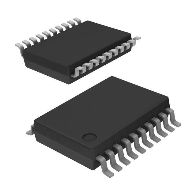
| 描述 | IC OCT TRANSP D-TYP LATCH 20SSOP闭锁 Tri-St Octal D-Type |
| 产品分类 | |
| 品牌 | Texas Instruments |
| 产品手册 | |
| 产品图片 |
|
| rohs | 符合RoHS无铅 / 符合限制有害物质指令(RoHS)规范要求 |
| 产品系列 | 逻辑集成电路,闭锁,Texas Instruments SN74ACT373DBR74ACT |
| 数据手册 | |
| 产品型号 | SN74ACT373DBR |
| 产品种类 | 闭锁 |
| 传播延迟时间 | 10 ns at 5 V |
| 低电平输出电流 | 32 mA |
| 供应商器件封装 | 20-SSOP |
| 其它名称 | 296-4420-6 |
| 包装 | Digi-Reel® |
| 单位重量 | 156.700 mg |
| 商标 | Texas Instruments |
| 安装类型 | 表面贴装 |
| 安装风格 | SMD/SMT |
| 封装 | Reel |
| 封装/外壳 | 20-SSOP(0.209",5.30mm 宽) |
| 封装/箱体 | SSOP-20 |
| 工作温度 | -40°C ~ 85°C |
| 工厂包装数量 | 2000 |
| 延迟时间-传播 | 8.5ns |
| 最大工作温度 | + 85 C |
| 最小工作温度 | - 40 C |
| 极性 | Non-Inverting |
| 标准包装 | 1 |
| 独立电路 | 1 |
| 电压-电源 | 4.5 V ~ 5.5 V |
| 电流-输出高,低 | 24mA,24mA |
| 电源电压-最大 | 5.5 V |
| 电源电压-最小 | 4.5 V |
| 电路 | 8:8 |
| 电路数量 | 8 Circuit |
| 系列 | SN74ACT373 |
| 输入线路数量 | 3 Line |
| 输出类型 | 三态 |
| 输出线路数量 | 1 Line |
| 逻辑类型 | D 型透明锁存器 |
| 逻辑系列 | 74ACT |
| 高电平输出电流 | - 24 mA |


- 商务部:美国ITC正式对集成电路等产品启动337调查
- 曝三星4nm工艺存在良率问题 高通将骁龙8 Gen1或转产台积电
- 太阳诱电将投资9.5亿元在常州建新厂生产MLCC 预计2023年完工
- 英特尔发布欧洲新工厂建设计划 深化IDM 2.0 战略
- 台积电先进制程称霸业界 有大客户加持明年业绩稳了
- 达到5530亿美元!SIA预计今年全球半导体销售额将创下新高
- 英特尔拟将自动驾驶子公司Mobileye上市 估值或超500亿美元
- 三星加码芯片和SET,合并消费电子和移动部门,撤换高东真等 CEO
- 三星电子宣布重大人事变动 还合并消费电子和移动部门
- 海关总署:前11个月进口集成电路产品价值2.52万亿元 增长14.8%


PDF Datasheet 数据手册内容提取
SN54ACT373, SN74ACT373 OCTAL D-TYPE TRANSPARENT LATCHES WITH 3-STATE OUTPUTS SCAS544E – OCTOBER 1995 – REVISED OCTOBER 2002 (cid:0) 4.5-V to 5.5-V V Operation SN54ACT373...J OR W PACKAGE CC (cid:0) SN74ACT373...DB, DW, N, NS, OR PW PACKAGE Inputs Accept Voltages to 5.5 V (TOP VIEW) (cid:0) Max t of 10 ns at 5 V pd (cid:0) Inputs Are TTL-Voltage Compatible OE 1 20 VCC 1Q 2 19 8Q description/ordering information 1D 3 18 8D 2D 4 17 7D These 8-bit latches feature 3-state outputs 2Q 5 16 7Q designed specifically for driving highly capacitive 3Q 6 15 6Q or relatively low-impedance loads. The devices 3D 7 14 6D are particularly suitable for implementing buffer 4D 8 13 5D registers, I/O ports, bidirectional bus drivers, and 4Q 9 12 5Q working registers. GND 10 11 LE The eight latches are D-type transparent latches. When the latch-enable (LE) input is high, the Q SN54ACT373...FK PACKAGE outputs follow the data (D) inputs. When LE is (TOP VIEW) taken low, the Q outputs are latched at the logic C levels set up at the D inputs. D Q E CQ 1 1 OV 8 A buffered output-enable (OE) input can be used 3 2 1 20 19 to place the eight outputs in either a normal logic 2D 4 18 8D state (high or low logic levels) or the 2Q 5 17 7D high-impedance state. In the high-impedance 3Q 6 16 7Q state, the outputs neither load nor drive the bus 3D 7 15 6Q lines significantly. The high-impedance state and 4D 8 14 6D increased drive provide the capability to drive bus 9 10 11 12 13 lines in bus-organized systems without need for Q D EQ D interface or pullup components. 4 N L5 5 G OE does not affect the internal operations of the latches. Old data can be retained or new data can be entered while the outputs are in the high-impedance state. To ensure the high-impedance state during power up or power down, OE should be tied to V through a pullup CC resistor; the minimum value of the resistor is determined by the current-sinking capability of the driver. ORDERING INFORMATION ORDERABLE TOP-SIDE TA PACKAGE† PART NUMBER MARKING PDIP – N Tube SN74ACT373N SN74ACT373N Tube SN74ACT373DW SSOOIICC – DDWW AACCTT337733 Tape and reel SN74ACT373DWR –4400°°CC ttoo 8855°°CC SOP – NS Tape and reel SN74ACT373NSR ACT373 SSOP – DB Tape and reel SN74ACT373DBR AD373 TSSOP – PW Tape and reel SN74ACT373PWR AD373 CDIP – J Tube SNJ54ACT373J SNJ54ACT373J –55°C to 125°C CFP – W Tube SNJ54ACT373W SNJ54ACT373W LCCC – FK Tube SNJ54ACT373FK SNJ54ACT373FK †Package drawings, standard packing quantities, thermal data, symbolization, and PCB design guidelines are available at www.ti.com/sc/package. Please be aware that an important notice concerning availability, standard warranty, and use in critical applications of TexasInstruments semiconductor products and disclaimers thereto appears at the end of this data sheet. PRODUCTION DATA information is current as of publication date. Copyright 2002, Texas Instruments Incorporated Products conform to specifications per the terms of Texas Instruments On products compliant to MIL-PRF-38535, all parameters are tested standard warranty. Production processing does not necessarily include unless otherwise noted. On all other products, production testing of all parameters. processing does not necessarily include testing of all parameters. POST OFFICE BOX 655303 • DALLAS, TEXAS 75265 1
SN54ACT373, SN74ACT373 OCTAL D-TYPE TRANSPARENT LATCHES WITH 3-STATE OUTPUTS SCAS544E – OCTOBER 1995 – REVISED OCTOBER 2002 FUNCTION TABLE (each latch) INPUTS OUTPUT OE LE D Q L H H H L H L L L L X Q0 H X X Z logic diagram (positive logic) 1 OE 11 LE C1 2 1Q 3 1D 1D To Seven Other Channels absolute maximum ratings over operating free-air temperature range (unless otherwise noted)† Supply voltage range, V . . . . . . . . . . . . . . . . . . . . . . . . . . . . . . . . . . . . . . . . . . . . . . . . . . . . . . . . . . –0.5 V to 7 V CC Input voltage range, V (see Note 1) . . . . . . . . . . . . . . . . . . . . . . . . . . . . . . . . . . . . . . . . . . . –0.5 V to V + 0.5 V I CC Output voltage range, V (see Note 1) . . . . . . . . . . . . . . . . . . . . . . . . . . . . . . . . . . . . . . . . –0.5 V to V + 0.5 V O CC Input clamp current, I (V < 0 or V > V . . . . . . . . . . . . . . . . . . . . . . . . . . . . . . . . . . . . . . . . . . . . . . . . ±20 mA IK I I CC) Output clamp current, I (V < 0 or V > V . . . . . . . . . . . . . . . . . . . . . . . . . . . . . . . . . . . . . . . . . . . . ±20 mA OK O O CC) Continuous output current, I (V = 0 to V ) . . . . . . . . . . . . . . . . . . . . . . . . . . . . . . . . . . . . . . . . . . . . . . ±50 mA O O CC Continuous current through V or GND . . . . . . . . . . . . . . . . . . . . . . . . . . . . . . . . . . . . . . . . . . . . . . . . . . ±200 mA CC Package thermal impedance, θ (see Note 2): DB package . . . . . . . . . . . . . . . . . . . . . . . . . . . . . . . . . 70°C/W JA DW package . . . . . . . . . . . . . . . . . . . . . . . . . . . . . . . . . 58°C/W N package . . . . . . . . . . . . . . . . . . . . . . . . . . . . . . . . . . . 69°C/W NS package . . . . . . . . . . . . . . . . . . . . . . . . . . . . . . . . . 60°C/W PW package . . . . . . . . . . . . . . . . . . . . . . . . . . . . . . . . . 83°C/W Storage temperature range, T . . . . . . . . . . . . . . . . . . . . . . . . . . . . . . . . . . . . . . . . . . . . . . . . . . . –65°C to 150°C stg †Stresses beyond those listed under “absolute maximum ratings” may cause permanent damage to the device. These are stress ratings only, and functional operation of the device at these or any other conditions beyond those indicated under “recommended operating conditions” is not implied. Exposure to absolute-maximum-rated conditions for extended periods may affect device reliability. NOTES: 1. The input and output voltage ratings may be exceeded if the input and output current ratings are observed. 2. The package thermal impedance is calculated in accordance with JESD 51-7. 2 POST OFFICE BOX 655303 • DALLAS, TEXAS 75265
SN54ACT373, SN74ACT373 OCTAL D-TYPE TRANSPARENT LATCHES WITH 3-STATE OUTPUTS SCAS544E – OCTOBER 1995 – REVISED OCTOBER 2002 recommended operating conditions (see Note 3) SN54ACT373 SN74ACT373 UUNNIITT MIN MAX MIN MAX VCC Supply voltage 4.5 5.5 4.5 5.5 V VIH High-level input voltage 2 2 V VIL Low-level input voltage 0.8 0.8 V VI Input voltage 0 VCC 0 VCC V VO Output voltage 0 VCC 0 VCC V IOH High-level output current –24 –24 mA IOL Low-level output current 24 24 mA ∆t/∆v Input transition rise or fall rate 8 8 ns/V TA Operating free-air temperature –55 125 –40 85 °C NOTE 3: All unused inputs of the device must be held at VCC or GND to ensure proper device operation. Refer to the TI application report Implications of Slow or Floating CMOS Inputs, literature number SCBA004. electrical characteristics over recommended operating free-air temperature range (unless otherwise noted) TA = 25°C SN54ACT373 SN74ACT373 PPAARRAAMMEETTEERR TTEESSTT CCOONNDDIITTIIOONNSS VVCCCC UUNNIITT MIN TYP MAX MIN MAX MIN MAX 4.5 V 4.4 4.49 4.4 4.4 IIOOHH == –5500 µµAA 5.5 V 5.4 5.49 5.4 5.4 4.5 V 3.86 3.7 3.76 VVOOHH IIOOHH == –2244 mmAA VV 5.5 V 4.86 4.7 4.76 IOH = –50 mA† 5.5 V 3.85 IOH = –75 mA† 5.5 V 3.85 4.5 V 0.1 0.1 0.1 IIOOLL == 5500 µµAA 5.5 V 0.1 0.1 0.1 4.5 V 0.36 0.44 0.44 VVOOLL IIOOLL == 2244 mmAA VV 5.5 V 0.36 0.44 0.44 IOL = 50 mA† 5.5 V 1.65 IOL = 75 mA† 5.5 V 1.65 IOZ VO = VCC or GND 5.5 V ±0.25 ±5 ±2.5 µA II VI = VCC or GND 5.5 V ±0.1 ±1 ±1 µA ICC VI = VCC or GND, IO = 0 5.5 V 4 80 40 µA One input at 3.4 V, ∆ICC‡ Other inputs at GND or VCC 5.5 V 0.6 1.5 1.5 mA Ci VI = VCC or GND 5 V 4.5 pF †Not more than one output should be tested at a time, and the duration of the test should not exceed 2 ms. ‡This is the increase in supply current for each input that is at one of the specified TTL voltage levels, rather than 0 V or VCC. timing requirements over recommended operating free-air temperature range, V = 5 V ± 0.5 V CC (unless otherwise noted) (see Figure 1) TA = 25°C SN54ACT373 SN74ACT373 UUNNIITT MIN MAX MIN MAX MIN MAX tw Pulse duration, LE high 7 8.5 8 ns tsu Setup time, data before LE↓ 7 8.5 8 ns th Hold time, data after LE↓ 0 1 1 ns POST OFFICE BOX 655303 • DALLAS, TEXAS 75265 3
SN54ACT373, SN74ACT373 OCTAL D-TYPE TRANSPARENT LATCHES WITH 3-STATE OUTPUTS SCAS544E – OCTOBER 1995 – REVISED OCTOBER 2002 switching characteristics over recommended operating free-air temperature range, V = 5 V ±0.5 V (unless otherwise noted) (see Figure 1) CC FROM TO TA = 25°C SN54ACT373 SN74ACT373 PPAARRAAMMEETTEERR UUNNIITT (INPUT) (OUTPUT) MIN TYP MAX MIN MAX MIN MAX tPLH 2.5 8.5 10 1.5 12.5 1.5 11.5 DD QQ nnss tPHL 2 8 10 1.5 12.5 1.5 11.5 tPLH 2.5 8.5 11 1.5 12.5 2 11.5 LLEE QQ nnss tPHL 2 8 10 1.5 11.5 1.5 11.5 tPZH 2 8 9.5 1.5 11.5 1.5 10.5 OOEE QQ nnss tPZL 2 7.5 9 1.5 11 1.5 10.5 tPHZ 2.5 9 11 1.5 14 2.5 12.5 OOEE QQ nnss tPLZ 1.5 7.5 8.5 1.5 11 1 10 operating characteristics, V = 5 V, T = 25°C CC A PARAMETER TEST CONDITIONS TYP UNIT Cpd Power dissipation capacitance CL = 50 pF, f = 1 MHz 40 pF 4 POST OFFICE BOX 655303 • DALLAS, TEXAS 75265
SN54ACT373, SN74ACT373 OCTAL D-TYPE TRANSPARENT LATCHES WITH 3-STATE OUTPUTS SCAS544E – OCTOBER 1995 – REVISED OCTOBER 2002 PARAMETER MEASUREMENT INFORMATION 2 × VCC TEST S1 From Output 500 Ω S1 Open tPLH/tPHL Open Under Test tPLZ/tPZL 2 × VCC CL = 50 pF 500 Ω tPHZ/tPZH Open (see Note A) 3 V Timing Input 1.5 V LOAD CIRCUIT 0 V th tsu 3 V tw Data Input 1.5 V 1.5 V 0 V 3 V VOLTAGE WAVEFORMS Input 1.5 V 1.5 V 0 V Output 3 V Control VOLTAGE WAVEFORMS 1.5 V 1.5 V (low-level enabling) 0 V tPZL tPLZ Output 3 V Waveform 1 ≈VCC Input 1.5 V 1.5 V S1 at 2 × VCC 50% VCC VOL + 0.3 V 0 V (see Note B) VOL tPLH tPHL tPZH tPHZ Output VOH Waveform 2 VOH Output 50% VCC 50% VCC S1 at Open 50% VCC VOH – 0.3 V VOL (see Note B) ≈0 V VOLTAGE WAVEFORMS VOLTAGE WAVEFORMS NOTES: A. CL includes probe and jig capacitance. B. Waveform 1 is for an output with internal conditions such that the output is low except when disabled by the output control. Waveform 2 is for an output with internal conditions such that the output is high except when disabled by the output control. C. All input pulses are supplied by generators having the following characteristics: PRR ≤ 1 MHz, ZO = 50 Ω, tr ≤ 2.5 ns, tf ≤ 2.5 ns. D. The outputs are measured one at a time with one input transition per measurement. Figure 1. Load Circuit and Voltage Waveforms POST OFFICE BOX 655303 • DALLAS, TEXAS 75265 5
PACKAGE OPTION ADDENDUM www.ti.com 6-Feb-2020 PACKAGING INFORMATION Orderable Device Status Package Type Package Pins Package Eco Plan Lead/Ball Finish MSL Peak Temp Op Temp (°C) Device Marking Samples (1) Drawing Qty (2) (6) (3) (4/5) 5962-87556012A ACTIVE LCCC FK 20 1 TBD POST-PLATE N / A for Pkg Type -55 to 125 5962- 87556012A SNJ54ACT 373FK 5962-8755601RA ACTIVE CDIP J 20 1 TBD Call TI N / A for Pkg Type -55 to 125 5962-8755601RA SNJ54ACT373J 5962-8755601SA ACTIVE CFP W 20 1 TBD Call TI N / A for Pkg Type -55 to 125 5962-8755601SA SNJ54ACT373W 5962-8755601VRA ACTIVE CDIP J 20 1 TBD Call TI N / A for Pkg Type -55 to 125 5962-8755601VR A SNV54ACT373J SN74ACT373DBR ACTIVE SSOP DB 20 2000 Green (RoHS NIPDAU Level-1-260C-UNLIM -40 to 85 AD373 & no Sb/Br) SN74ACT373DW ACTIVE SOIC DW 20 25 Green (RoHS NIPDAU Level-1-260C-UNLIM -40 to 85 ACT373 & no Sb/Br) SN74ACT373DWR ACTIVE SOIC DW 20 2000 Green (RoHS NIPDAU Level-1-260C-UNLIM -40 to 85 ACT373 & no Sb/Br) SN74ACT373N ACTIVE PDIP N 20 20 Pb-Free NIPDAU N / A for Pkg Type -40 to 85 SN74ACT373N (RoHS) SN74ACT373NSR ACTIVE SO NS 20 2000 Green (RoHS NIPDAU Level-1-260C-UNLIM -40 to 85 ACT373 & no Sb/Br) SN74ACT373PW ACTIVE TSSOP PW 20 70 Green (RoHS NIPDAU Level-1-260C-UNLIM -40 to 85 AD373 & no Sb/Br) SN74ACT373PWR ACTIVE TSSOP PW 20 2000 Green (RoHS NIPDAU Level-1-260C-UNLIM -40 to 85 AD373 & no Sb/Br) SNJ54ACT373FK ACTIVE LCCC FK 20 1 TBD POST-PLATE N / A for Pkg Type -55 to 125 5962- 87556012A SNJ54ACT 373FK SNJ54ACT373J ACTIVE CDIP J 20 1 TBD Call TI N / A for Pkg Type -55 to 125 5962-8755601RA SNJ54ACT373J SNJ54ACT373W ACTIVE CFP W 20 1 TBD Call TI N / A for Pkg Type -55 to 125 5962-8755601SA SNJ54ACT373W (1) The marketing status values are defined as follows: Addendum-Page 1
PACKAGE OPTION ADDENDUM www.ti.com 6-Feb-2020 ACTIVE: Product device recommended for new designs. LIFEBUY: TI has announced that the device will be discontinued, and a lifetime-buy period is in effect. NRND: Not recommended for new designs. Device is in production to support existing customers, but TI does not recommend using this part in a new design. PREVIEW: Device has been announced but is not in production. Samples may or may not be available. OBSOLETE: TI has discontinued the production of the device. (2) RoHS: TI defines "RoHS" to mean semiconductor products that are compliant with the current EU RoHS requirements for all 10 RoHS substances, including the requirement that RoHS substance do not exceed 0.1% by weight in homogeneous materials. Where designed to be soldered at high temperatures, "RoHS" products are suitable for use in specified lead-free processes. TI may reference these types of products as "Pb-Free". RoHS Exempt: TI defines "RoHS Exempt" to mean products that contain lead but are compliant with EU RoHS pursuant to a specific EU RoHS exemption. Green: TI defines "Green" to mean the content of Chlorine (Cl) and Bromine (Br) based flame retardants meet JS709B low halogen requirements of <=1000ppm threshold. Antimony trioxide based flame retardants must also meet the <=1000ppm threshold requirement. (3) MSL, Peak Temp. - The Moisture Sensitivity Level rating according to the JEDEC industry standard classifications, and peak solder temperature. (4) There may be additional marking, which relates to the logo, the lot trace code information, or the environmental category on the device. (5) Multiple Device Markings will be inside parentheses. Only one Device Marking contained in parentheses and separated by a "~" will appear on a device. If a line is indented then it is a continuation of the previous line and the two combined represent the entire Device Marking for that device. (6) Lead/Ball Finish - Orderable Devices may have multiple material finish options. Finish options are separated by a vertical ruled line. Lead/Ball Finish values may wrap to two lines if the finish value exceeds the maximum column width. Important Information and Disclaimer:The information provided on this page represents TI's knowledge and belief as of the date that it is provided. TI bases its knowledge and belief on information provided by third parties, and makes no representation or warranty as to the accuracy of such information. Efforts are underway to better integrate information from third parties. TI has taken and continues to take reasonable steps to provide representative and accurate information but may not have conducted destructive testing or chemical analysis on incoming materials and chemicals. TI and TI suppliers consider certain information to be proprietary, and thus CAS numbers and other limited information may not be available for release. In no event shall TI's liability arising out of such information exceed the total purchase price of the TI part(s) at issue in this document sold by TI to Customer on an annual basis. OTHER QUALIFIED VERSIONS OF SN54ACT373, SN54ACT373-SP, SN74ACT373 : •Catalog: SN74ACT373, SN54ACT373 •Enhanced Product: SN74ACT373-EP, SN74ACT373-EP •Military: SN54ACT373 •Space: SN54ACT373-SP Addendum-Page 2
PACKAGE OPTION ADDENDUM www.ti.com 6-Feb-2020 NOTE: Qualified Version Definitions: •Catalog - TI's standard catalog product •Enhanced Product - Supports Defense, Aerospace and Medical Applications •Military - QML certified for Military and Defense Applications •Space - Radiation tolerant, ceramic packaging and qualified for use in Space-based application Addendum-Page 3
PACKAGE MATERIALS INFORMATION www.ti.com 6-May-2017 TAPE AND REEL INFORMATION *Alldimensionsarenominal Device Package Package Pins SPQ Reel Reel A0 B0 K0 P1 W Pin1 Type Drawing Diameter Width (mm) (mm) (mm) (mm) (mm) Quadrant (mm) W1(mm) SN74ACT373DBR SSOP DB 20 2000 330.0 16.4 8.2 7.5 2.5 12.0 16.0 Q1 SN74ACT373DWR SOIC DW 20 2000 330.0 24.4 10.8 13.3 2.7 12.0 24.0 Q1 SN74ACT373NSR SO NS 20 2000 330.0 24.4 8.4 13.0 2.5 12.0 24.0 Q1 SN74ACT373PWR TSSOP PW 20 2000 330.0 16.4 6.95 7.1 1.6 8.0 16.0 Q1 PackMaterials-Page1
PACKAGE MATERIALS INFORMATION www.ti.com 6-May-2017 *Alldimensionsarenominal Device PackageType PackageDrawing Pins SPQ Length(mm) Width(mm) Height(mm) SN74ACT373DBR SSOP DB 20 2000 367.0 367.0 38.0 SN74ACT373DWR SOIC DW 20 2000 367.0 367.0 45.0 SN74ACT373NSR SO NS 20 2000 367.0 367.0 45.0 SN74ACT373PWR TSSOP PW 20 2000 367.0 367.0 38.0 PackMaterials-Page2
None
PACKAGE OUTLINE DB0020A SSOP - 2 mm max height SCALE 2.000 SMALL OUTLINE PACKAGE C 8.2 TYP 7.4 A 0.1 C PIN 1 INDEX AREA SEATING PLANE 18X 0.65 20 1 2X 7.5 5.85 6.9 NOTE 3 10 11 0.38 20X 0.22 5.6 B 0.1 C A B 5.0 NOTE 4 2 MAX (0.15) TYP 0.25 SEE DETAIL A GAGE PLANE 0 -8 0.95 0.05 MIN 0.55 DETA 15AIL A TYPICAL 4214851/B 08/2019 NOTES: 1. All linear dimensions are in millimeters. Any dimensions in parenthesis are for reference only. Dimensioning and tolerancing per ASME Y14.5M. 2. This drawing is subject to change without notice. 3. This dimension does not include mold flash, protrusions, or gate burrs. Mold flash, protrusions, or gate burrs shall not exceed 0.15 mm per side. 4. This dimension does not include interlead flash. Interlead flash shall not exceed 0.25 mm per side. 5. Reference JEDEC registration MO-150. www.ti.com
EXAMPLE BOARD LAYOUT DB0020A SSOP - 2 mm max height SMALL OUTLINE PACKAGE 20X (1.85) SYMM (R0.05) TYP 1 20X (0.45) 20 SYMM 18X (0.65) 10 11 (7) LAND PATTERN EXAMPLE EXPOSED METAL SHOWN SCALE: 10X SOLDER MASK METAL METAL UNDER SOLDER MASK OPENING SOLDER MASK OPENING EXPOSED METAL EXPOSED METAL 0.07 MAX 0.07 MIN ALL AROUND ALL AROUND NON-SOLDER MASK SOLDER MASK DEFINED DEFINED (PREFERRED) SOLDE15.000 R MASK DETAILS 4214851/B 08/2019 NOTES: (continued) 6. Publication IPC-7351 may have alternate designs. 7. Solder mask tolerances between and around signal pads can vary based on board fabrication site. www.ti.com
EXAMPLE STENCIL DESIGN DB0020A SSOP - 2 mm max height SMALL OUTLINE PACKAGE 20X (1.85) SYMM (R0.05) TYP 1 20X (0.45) 20 SYMM 18X (0.65) 10 11 (7) SOLDER PASTE EXAMPLE BASED ON 0.125 mm THICK STENCIL SCALE: 10X 4214851/B 08/2019 NOTES: (continued) 8. Laser cutting apertures with trapezoidal walls and rounded corners may offer better paste release. IPC-7525 may have alternate design recommendations. 9. Board assembly site may have different recommendations for stencil design. www.ti.com
None
None
None
None
None
PACKAGE OUTLINE DW0020A SOIC - 2.65 mm max height SCALE 1.200 SOIC C 10.63 SEATING PLANE TYP 9.97 A PIN 1 ID 0.1 C AREA 18X 1.27 20 1 13.0 2X 12.6 11.43 NOTE 3 10 11 0.51 20X 7.6 0.31 2.65 MAX B 7.4 0.25 C A B NOTE 4 0.33 TYP 0.10 0.25 SEE DETAIL A GAGE PLANE 0.3 1.27 0 - 8 0.1 0.40 DETAIL A TYPICAL 4220724/A 05/2016 NOTES: 1. All linear dimensions are in millimeters. Dimensions in parenthesis are for reference only. Dimensioning and tolerancing per ASME Y14.5M. 2. This drawing is subject to change without notice. 3. This dimension does not include mold flash, protrusions, or gate burrs. Mold flash, protrusions, or gate burrs shall not exceed 0.15 mm per side. 4. This dimension does not include interlead flash. Interlead flash shall not exceed 0.43 mm per side. 5. Reference JEDEC registration MS-013. www.ti.com
EXAMPLE BOARD LAYOUT DW0020A SOIC - 2.65 mm max height SOIC 20X (2) SYMM 1 20 20X (0.6) 18X (1.27) SYMM (R0.05) TYP 10 11 (9.3) LAND PATTERN EXAMPLE SCALE:6X SOOPLEDNEINRG MASK METAL MSOELTDAEL RU NMDAESRK SOOPLEDNEINRG MASK 0.07 MAX 0.07 MIN ALL AROUND ALL AROUND NON SOLDER MASK SOLDER MASK DEFINED DEFINED SOLDER MASK DETAILS 4220724/A 05/2016 NOTES: (continued) 6. Publication IPC-7351 may have alternate designs. 7. Solder mask tolerances between and around signal pads can vary based on board fabrication site. www.ti.com
EXAMPLE STENCIL DESIGN DW0020A SOIC - 2.65 mm max height SOIC 20X (2) SYMM 1 20 20X (0.6) 18X (1.27) SYMM 10 11 (9.3) SOLDER PASTE EXAMPLE BASED ON 0.125 mm THICK STENCIL SCALE:6X 4220724/A 05/2016 NOTES: (continued) 8. Laser cutting apertures with trapezoidal walls and rounded corners may offer better paste release. IPC-7525 may have alternate design recommendations. 9. Board assembly site may have different recommendations for stencil design. www.ti.com
None
IMPORTANTNOTICEANDDISCLAIMER TI PROVIDES TECHNICAL AND RELIABILITY DATA (INCLUDING DATASHEETS), DESIGN RESOURCES (INCLUDING REFERENCE DESIGNS), APPLICATION OR OTHER DESIGN ADVICE, WEB TOOLS, SAFETY INFORMATION, AND OTHER RESOURCES “AS IS” AND WITH ALL FAULTS, AND DISCLAIMS ALL WARRANTIES, EXPRESS AND IMPLIED, INCLUDING WITHOUT LIMITATION ANY IMPLIED WARRANTIES OF MERCHANTABILITY, FITNESS FOR A PARTICULAR PURPOSE OR NON-INFRINGEMENT OF THIRD PARTY INTELLECTUAL PROPERTY RIGHTS. These resources are intended for skilled developers designing with TI products. You are solely responsible for (1) selecting the appropriate TI products for your application, (2) designing, validating and testing your application, and (3) ensuring your application meets applicable standards, and any other safety, security, or other requirements. These resources are subject to change without notice. TI grants you permission to use these resources only for development of an application that uses the TI products described in the resource. Other reproduction and display of these resources is prohibited. No license is granted to any other TI intellectual property right or to any third party intellectual property right. TI disclaims responsibility for, and you will fully indemnify TI and its representatives against, any claims, damages, costs, losses, and liabilities arising out of your use of these resources. TI’s products are provided subject to TI’s Terms of Sale (www.ti.com/legal/termsofsale.html) or other applicable terms available either on ti.com or provided in conjunction with such TI products. TI’s provision of these resources does not expand or otherwise alter TI’s applicable warranties or warranty disclaimers for TI products. Mailing Address: Texas Instruments, Post Office Box 655303, Dallas, Texas 75265 Copyright © 2020, Texas Instruments Incorporated