ICGOO在线商城 > 集成电路(IC) > 逻辑 - 缓冲器,驱动器,接收器,收发器 > SN74ABT541BDBR

 Datasheet下载
- 型号: SN74ABT541BDBR
- 制造商: Texas Instruments
- 库位|库存: xxxx|xxxx
- 要求:
| 数量阶梯 | 香港交货 | 国内含税 |
| +xxxx | $xxxx | ¥xxxx |
查看当月历史价格
查看今年历史价格
SN74ABT541BDBR产品简介:
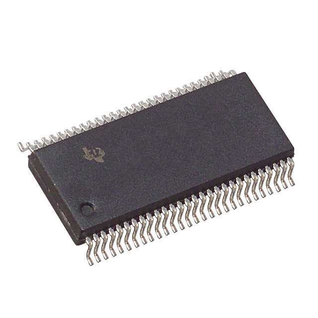
ICGOO电子元器件商城为您提供SN74ABT541BDBR由Texas Instruments设计生产,在icgoo商城现货销售,并且可以通过原厂、代理商等渠道进行代购。 SN74ABT541BDBR价格参考¥5.00-¥11.27。Texas InstrumentsSN74ABT541BDBR封装/规格:逻辑 - 缓冲器,驱动器,接收器,收发器, Buffer, Non-Inverting 1 Element 8 Bit per Element 3-State Output 20-SSOP。您可以下载SN74ABT541BDBR参考资料、Datasheet数据手册功能说明书,资料中有SN74ABT541BDBR 详细功能的应用电路图电压和使用方法及教程。
SN74ABT541BDBR 是由 Texas Instruments 生产的一款逻辑缓冲器、驱动器、接收器和收发器,属于 74 系列逻辑器件。该型号主要用于在数字电路中实现数据传输、信号转换和电平转换等功能。以下是其主要应用场景:

 1. 总线接口与扩展
SN74ABT541BDBR 可以用作双向总线收发器,适用于需要扩展或隔离数据总线的应用。它支持 8 位数据传输,并且可以在两个方向上进行数据通信。例如,在计算机系统中,它可以用于扩展内存总线或外设接口,确保数据在不同模块之间可靠传输。

 2. 电平转换
该器件支持 3.3V 和 5V 的逻辑电平转换,适用于混合电压系统的应用。例如,在嵌入式系统中,某些微控制器可能工作在 3.3V 电平,而外部设备或传感器可能工作在 5V 电平。SN74ABT541BDBR 可以在这两种电平之间进行无缝转换,确保信号的正确传输。

 3. 信号增强与驱动
在长距离或高噪声环境下,信号可能会衰减或受到干扰。SN74ABT541BDBR 具有较强的驱动能力,可以增强信号强度,确保信号在传输过程中不失真。它适用于工业控制、自动化设备等需要稳定信号传输的场合。

 4. 多路复用与隔离
该器件可以通过使能引脚(OE)控制数据的传输方向和状态,因此可以用于多路复用或隔离电路。例如,在多主机系统中,不同的主控设备可以通过 SN74ABT541BDBR 来共享同一总线,避免信号冲突。

 5. 低功耗设计
SN74ABT541BDBR 采用 ABT(Advanced BiCMOS Technology)工艺制造,具有较低的静态功耗,适合对功耗敏感的应用场景,如便携式设备或电池供电系统。

 总结
SN74ABT541BDBR 在数字系统中扮演着重要的角色,尤其适用于需要双向数据传输、电平转换、信号增强以及多路复用的应用。它广泛应用于计算机、通信、工业控制等领域,能够有效提高系统的稳定性和可靠性。
| 参数 | 数值 |
| 产品目录 | 集成电路 (IC)半导体 |
| 描述 | IC BUFF/DVR TRI-ST 8BIT 20SSOP缓冲器和线路驱动器 Tri-State Octal |
| 产品分类 | |
| 品牌 | Texas Instruments |
| 产品手册 | |
| 产品图片 |
|
| rohs | 符合RoHS无铅 / 符合限制有害物质指令(RoHS)规范要求 |
| 产品系列 | 逻辑集成电路,缓冲器和线路驱动器,Texas Instruments SN74ABT541BDBR74ABT |
| 数据手册 | |
| 产品型号 | SN74ABT541BDBR |
| 产品目录页面 | |
| 产品种类 | 缓冲器和线路驱动器 |
| 传播延迟时间 | 3.5 ns at 5 V |
| 低电平输出电流 | 64 mA |
| 供应商器件封装 | 20-SSOP |
| 元件数 | 1 |
| 其它名称 | 296-4025-1 |
| 包装 | 剪切带 (CT) |
| 单位重量 | 156.700 mg |
| 商标 | Texas Instruments |
| 安装类型 | 表面贴装 |
| 安装风格 | SMD/SMT |
| 封装 | Reel |
| 封装/外壳 | 20-SSOP(0.209",5.30mm 宽) |
| 封装/箱体 | SSOP-20 |
| 工作温度 | -40°C ~ 85°C |
| 工厂包装数量 | 2000 |
| 最大工作温度 | + 85 C |
| 最小工作温度 | - 40 C |
| 极性 | Non-Inverting |
| 标准包装 | 1 |
| 每元件位数 | 8 |
| 每芯片的通道数量 | 8 |
| 电压-电源 | 4.5 V ~ 5.5 V |
| 电流-输出高,低 | 32mA,64mA |
| 电源电压-最大 | 5.5 V |
| 电源电压-最小 | 4.5 V |
| 电源电流 | 0.25 mA |
| 系列 | SN74ABT541B |
| 输入线路数量 | 8 |
| 输出类型 | 3-State |
| 输出线路数量 | 8 |
| 逻辑类型 | 缓冲器/线路驱动器,非反相 |
| 逻辑系列 | ABT |
| 高电平输出电流 | - 32 mA |


- 商务部:美国ITC正式对集成电路等产品启动337调查
- 曝三星4nm工艺存在良率问题 高通将骁龙8 Gen1或转产台积电
- 太阳诱电将投资9.5亿元在常州建新厂生产MLCC 预计2023年完工
- 英特尔发布欧洲新工厂建设计划 深化IDM 2.0 战略
- 台积电先进制程称霸业界 有大客户加持明年业绩稳了
- 达到5530亿美元!SIA预计今年全球半导体销售额将创下新高
- 英特尔拟将自动驾驶子公司Mobileye上市 估值或超500亿美元
- 三星加码芯片和SET,合并消费电子和移动部门,撤换高东真等 CEO
- 三星电子宣布重大人事变动 还合并消费电子和移动部门
- 海关总署:前11个月进口集成电路产品价值2.52万亿元 增长14.8%


PDF Datasheet 数据手册内容提取
SN54ABT541, SN74ABT541B OCTAL BUFFERS/DRIVERS WITH 3-STATE OUTPUTS www.ti.com SCBS093L–DECEMBER1993–REVISEDDECEMBER2006 FEATURES • State-of-the-ArtEPIC-IIB™BiCMOSDesign SN54ABT541...J OR W PACKAGE SignificantlyReducesPowerDissipation SN74ABT541B...DB, DW, N, OR PW PACKAGE (TOPVIEW) • Latch-UpPerformanceExceeds500mAPer JEDECStandardJESD-17 OE1 1 20 V CC • TypicalV (OutputGroundBounce)<1Vat A1 2 19 OE2 OLP A2 3 18 Y1 V =5V,T =25(cid:176) C CC A A3 4 17 Y2 • High-ImpedanceStateDuringPowerUpand A4 5 16 Y3 A5 6 15 Y4 PowerDown A6 7 14 Y5 • High-DriveOutputs(–32-mAI ,64-mAI ) A7 8 13 Y6 OH OL • PackageOptionsIncludePlasticSmall-Outline A8 9 12 Y7 GND 10 11 Y8 (DW),ShrinkSmall-Outline(DB),andThin ShrinkSmall-Outline(PW)Packages,Ceramic SN54ABT541...FK PACKAGE ChipCarriers(FK),CeramicFlat(W)Package, (TOPVIEW) andPlastic(N)andCeramic(J)DIPs 1 2 A2 A1 OE VCC OE 3 2 1 20 19 A3 4 18 Y1 A4 5 17 Y2 A5 6 16 Y3 A6 7 15 Y4 A7 8 14 Y5 9 10 11 12 13 8 D8 7 6 A NY Y Y G DESCRIPTION/ORDERING INFORMATION The SN54ABT541 and SN74ABT541B octal buffers and line drivers are ideal for driving bus lines or buffering memory address registers. The devices feature inputs and outputs on opposite sides of the package to facilitate printedcircuitboardlayout. ORDERINGINFORMATION T PACKAGE(1) ORDERABLEPARTNUMBER TOP-SIDEMARKING A PDIP–N Reelof1000 SN74ABT541BN SN74ABT541BN Tubeof25 SN74ABT541BDW SOIC–DW ABT541B Reelof2000 SN74ABT541BDWR –40(cid:176) Cto85(cid:176) C SN74ABT541BDBR SSOP–DB Reelof2000 AB541B SN74ABT541BDBRG4 Reelof1050 SN74ABT541BPW TSSOP–PW AB541B Reelof2000 SN74ABT541BPWR CDIP–J Reelof1000 SNJ54ABT541J SNJ54ABT541J –55(cid:176) Cto125(cid:176) C CFP–W Reelof510 SNJ54ABT541W SNJ54ABT541W LCCC–FK Reelof2200 SNJ54ABT541FK SNJ54ABT541FK (1) Packagedrawings,standardpackingquantities,thermaldata,symbolization,andPCBdesignguidelinesareavailableat www.ti.com/sc/package. Pleasebeawarethatanimportantnoticeconcerningavailability,standardwarranty,anduseincriticalapplicationsofTexas Instrumentssemiconductorproductsanddisclaimerstheretoappearsattheendofthisdatasheet. EPIC-IIBisatrademarkofTexasInstruments. PRODUCTIONDATAinformationiscurrentasofpublicationdate. Copyright©1993–2006,TexasInstrumentsIncorporated Products conform to specifications per the terms of the Texas Instruments standard warranty. Production processing does not necessarilyincludetestingofallparameters.
SN54ABT541, SN74ABT541B OCTAL BUFFERS/DRIVERS WITH 3-STATE OUTPUTS www.ti.com SCBS093L–DECEMBER1993–REVISEDDECEMBER2006 DESCRIPTION/ORDERING INFORMATION (CONTINUED) The 3-state control gate is a two-input AND gate with active-low inputs so that if either output-enable (OE1 or OE2)inputishigh,alleightoutputsareinthehigh-impedancestate. When VCC is between 0 and 2.1 V, the device is in the high-impedance state during power up or power down. However, to ensure the high-impedance state above 2.1 V, OE should be tied to VCC through a pullup resistor; theminimumvalueoftheresistorisdeterminedbythecurrent-sinkingcapabilityofthedriver. The SN54ABT541 is characterized for operation over the full military temperature range of –55(cid:176) C to 125(cid:176) C. The SN74ABT541Bischaracterizedforoperationfrom–40(cid:176) Cto85(cid:176) C. FUNCTIONTABLE INPUTS OUTPUTS OE1 OE2 A Y L L L L L L H H H X X Z X H X Z LOGIC SYMBOL(1) LOGICDIAGRAM(POSITIVELOGIC) 1 & EN OE1 1 OE1 19 19 OE2 OE2 2 18 2 18 A1 Y1 A1 1 Y1 3 17 A2 Y2 4 16 To Seven Other Channels A3 Y3 5 15 A4 Y4 6 14 A5 Y5 7 13 A6 Y6 8 12 A7 Y7 9 11 A8 Y8 (1) This symbol is in accordance with ANSI/IEEE Std 91-1984 and IEC Publication617-12. 2 SubmitDocumentationFeedback
SN54ABT541, SN74ABT541B OCTAL BUFFERS/DRIVERS WITH 3-STATE OUTPUTS www.ti.com SCBS093L–DECEMBER1993–REVISEDDECEMBER2006 Absolute Maximum Ratings(1) overrecommendedoperatingfree-airtemperaturerange(unlessotherwisenoted) MIN MAX UNIT V Supplyvoltagerange –0.5 7 V CC V Inputvoltagerange(2) –0.5 7 V I V Voltagerangeappliedtoanyoutputinthehighorpower-offstate –0.5 5.5 V O I Currentintoanyoutputinthelowstate SN54ABT541 96 O mA SN74ABT541B 128 I Inputclampcurrent V <0 –18 mA IK I I Outputclampcurrent V <0 –50 mA OK O q Packagethermalimpedance(3) DBpackage 115 JA DWpackage 97 (cid:176) C/W Npackage 67 PWpackage 128 T Storagetemperaturerange –65 150 (cid:176) C stg (1) Stressesbeyondthoselistedunder“absolutemaximumratings”maycausepermanentdamagetothedevice.Thesearestressratings only,andfunctionaloperationofthedeviceattheseoranyotherconditionsbeyondthoseindicatedunder“recommendedoperating conditions”isnotimplied.Exposuretoabsolute-maximum-ratedconditionsforextendedperiodsmayaffectdevicereliability. (2) Theinputandoutputnegative-voltageratingsmaybeexceedediftheinputandoutputclamp-currentratingsareobserved. (3) ThepackagethermalimpedanceiscalculatedinaccordancewithJESD51,exceptforthrough-holepackages,whichuseatracelength ofzero. Recommended Operating Conditions(1) overrecommendedoperatingfree-airtemperaturerange(unlessotherwisenoted) SN54ABT541 SN74ABT541B UNIT MIN MAX MIN MAX V Supplyvoltage 4.5 5.5 4.5 5.5 V CC V High-levelinputvoltage 2 2 V IH V Low-levelinputvoltage 0.8 0.8 V IL I High-leveloutputcurrent –24 –32 mA OH I Low-leveloutputcurrent 48 64 mA OL D t/D v Inputtransitionriseorfallrate 5 5 ns/V D t/D V Power-upramprate 200 m s/V CC T Operatingfree-airtemperature –55 125 –40 85 (cid:176) C A (1) AllunusedinputsofthedevicemustbeheldatV orGNDtoensureproperdeviceoperation.RefertotheTIapplicationreport, CC ImplicationsofSloworFloatingCMOSInputs,literaturenumberSCBA004. SubmitDocumentationFeedback 3
SN54ABT541, SN74ABT541B OCTAL BUFFERS/DRIVERS WITH 3-STATE OUTPUTS www.ti.com SCBS093L–DECEMBER1993–REVISEDDECEMBER2006 Electrical Characteristics overoperatingfree-airtemperaturerange(unlessotherwisenoted) T =25(cid:176) C SN54ABT51 SN74ABT541B A PARAMETER TESTCONDITIONS UNIT MIN TYP(1) MAX MIN MAX MIN MAX V V =4.5V, I =–18mA –1.2 –1.2 –1.2 V IK CC I V V =4.5V, I =–3mA 2.5 2.5 2.5 OH CC OH V =5V, I =–3mA 3 3 3 CC OH V V =4.5V, I =–24mA 2 2 CC OH I =–32mA 2(2) 2 OH V V =4.5V, I =48mA 0.55 0.55 OL CC OL VV I =64mA 0.55(2) 0.55 OL V 100 mV hys I V =5.5V, V =V orGND – 1 – 1 – 1 m A I CC I CC I V =0to2.1V,V =0.5Vto2.7V,OE=X – 50(3) – 50(3) – 50 m A OZPU CC O I V =2.1Vto0,V =0.5Vto2.7V,OE=X – 50(3) – 50(3) – 50 m A OZPD CC O I V =5.5V, V =2.7V 10 10 10 m A OZH CC O I V =5.5V, V =0.5V –10 –10 –10 m A OZL CC O I V =0V, V orV £ 4.5V – 100 – 100 m A off CC I O I V =5.5V,V =5.5V, Outputshigh 50 50 m A CEX CC O I V =5.5V(4), V =2.5V –50 –140 –180 –50 –180 –50 –180 mA O CC O I V =5.5V, Outputshigh 5 250 250 250 m A CC CC I =0V, O Outputslow 22 30 30 30 mA V =V orGND I CC Outputsdisabled 1 250 250 250 m A D I V =5.5V, Outputsenabled 1.5 1.5 1.5 mA CC CC Oneinputat3.4V, Outputsdisabled 50 50 50 m A OtherinputsatV or CC GND(5) ControlInputs 1.5 1.2 1.5 mA C V =2.5Vor0.5V 3 pF i I C V =2.5Vor0.5V 6 pF o O (1) AlltypicalvaluesareatV =5V. CC (2) OnproductscomplianttoMIL-PRF-38535,thisparameterdoesnotapply. (3) OnproductscomplianttoMIL-PRF-38535,thisparameterisnotproductiontested. (4) Notmorethanoneoutputshouldbetestedatatime,andthedurationofthetestshouldnotexceedonesecond. (5) ThisistheincreaseinsupplycurrentforeachinputthatisatthespecifiedTTLvoltagelevelratherthanV orGND. CC 4 SubmitDocumentationFeedback
SN54ABT541, SN74ABT541B OCTAL BUFFERS/DRIVERS WITH 3-STATE OUTPUTS www.ti.com SCBS093L–DECEMBER1993–REVISEDDECEMBER2006 Switching Characteristics, SN54ABT541 overrecommendedrangesofsupplyvoltageandoperatingfree-airtemperature,C =50pF(unlessotherwisenoted) L (seeFigure1) VCC=5V, PARAMETER FROM TO TA=25(cid:176) C UNIT (INPUT) (OUTPUT) MIN TYP MAX MIN MAX t 1 2.6 4.1 1 4.6 PLH A Y ns t 1 2.9 4.2 1 4.7 PHL t 1.1 3.1 4.8 1.1 5.4 PZH OE Y ns t 2.1 4.4 5.9 2.1 7 PZL t 2.1 5.1 6.6 2.1 7.5 PHZ OE Y ns t 1.7 4.7 6.2 1.7 6.7 PLZ Switching Characteristics, SN74ABT541B overrecommendedrangesofsupplyvoltageandoperatingfree-airtemperature,C =50pF(unlessotherwisenoted) L (seeFigure1) VCC=5V, PARAMETER FROM TO TA=25(cid:176) C UNIT (INPUT) (OUTPUT) MIN TYP MAX MIN MAX t 1 2 3.2 1 3.9 PLH A Y ns t 1 2.6 3.5 1 3.9 PHL t 2 3.5 4.5 2 4 PZH OE Y ns t 1.9 4 5.1 1.9 5.9 PZL t 2.2 4.4 5.4 2.2 5.8 PHZ OE Y ns t 1.5 3 4 1.5 4.4 PLZ t (1) 0.5 0.5 ns sk(o) (1) Skewbetweenanytwooutputsofthesamepackageswitchinginthesamedirection. SubmitDocumentationFeedback 5
SN54ABT541, SN74ABT541B OCTAL BUFFERS/DRIVERS WITH 3-STATE OUTPUTS www.ti.com SCBS093L–DECEMBER1993–REVISEDDECEMBER2006 PARAMETER MEASURMENT INFORMATION 7 V 500Ω S1 Open TEST S1 From Output Under Test GND tPLH/tPHL Open C = 50 pF t /t 7 V (seeL NoteA) 500Ω tPLZ/tPZL Open PHZ PZH LOAD CIRCUIT 3 V Timing Input 1.5 V 0 V t W 3 V tsu th 3 V Input 1.5 V 1.5 V Data Input 1.5 V 1.5 V 0 V 0 V VOLTAGE WAVEFORMS VOLTAGE WAVEFORMS PULSE DURATION SETUPAND HOLD TIMES 3 V 3 V Input 1.5 V 1.5 V Output 1.5 V 1.5 V Control 0 V 0 V t t t t PLH PHL PZL PLZ V Output 3.5 V Output VM 1.5 V OH WaSve1f oart m7 V1 1.5 V V + 0.3 V VOL (see Note B) OL V OL t t PHL PLH t t PZH PHZ Output 1.5 V 1.5 V VOH WaveOfourtmpu 2t V VOH–0.3 V VOH VOL (sSe1e aNt oOtep eBn) M »0 V VOLTAGE WAVEFORMS VOLTAGE WAVEFORMS PROPAGATION DELAYTIMES ENABLEAND DISABLE TIMES INVERTINGAND NONINVERTING OUTPUTS LOW-AND HIGH-LEVELENABLING NOTES: A. C includes probe and jig capacitance. L B. Waveform 1 is for an output with internal conditions such that the output is low, except when disabled by the output control. Waveform 2 is for an output with internal conditions such that the output is high, except when disabled by the output control. C. All input pulses are supplied by generators having the following characteristics: PRR£10 MHz, Z = 50Ω, t £2.5 ns, O r t £2.5 ns. f D. The outputs are measured one at a time, with one transition per measurement. Figure1.LoadCircuitandVoltageWaveforms 6 SubmitDocumentationFeedback
PACKAGE OPTION ADDENDUM www.ti.com 6-Feb-2020 PACKAGING INFORMATION Orderable Device Status Package Type Package Pins Package Eco Plan Lead/Ball Finish MSL Peak Temp Op Temp (°C) Device Marking Samples (1) Drawing Qty (2) (6) (3) (4/5) 5962-9471801Q2A ACTIVE LCCC FK 20 1 TBD POST-PLATE N / A for Pkg Type -55 to 125 5962- 9471801Q2A SNJ54 ABT541FK 5962-9471801QRA ACTIVE CDIP J 20 1 TBD Call TI N / A for Pkg Type -55 to 125 5962-9471801QR A SNJ54ABT541J 5962-9471801QSA ACTIVE CFP W 20 1 TBD Call TI N / A for Pkg Type -55 to 125 5962-9471801QS A SNJ54ABT541W SN74ABT541BDBR ACTIVE SSOP DB 20 2000 Green (RoHS NIPDAU Level-1-260C-UNLIM -40 to 85 AB541B & no Sb/Br) SN74ABT541BDBRE4 ACTIVE SSOP DB 20 2000 Green (RoHS NIPDAU Level-1-260C-UNLIM -40 to 85 AB541B & no Sb/Br) SN74ABT541BDBRG4 ACTIVE SSOP DB 20 2000 Green (RoHS NIPDAU Level-1-260C-UNLIM -40 to 85 AB541B & no Sb/Br) SN74ABT541BDW ACTIVE SOIC DW 20 25 Green (RoHS NIPDAU Level-1-260C-UNLIM -40 to 85 ABT541B & no Sb/Br) SN74ABT541BDWR ACTIVE SOIC DW 20 2000 Green (RoHS NIPDAU Level-1-260C-UNLIM -40 to 85 ABT541B & no Sb/Br) SN74ABT541BDWRE4 ACTIVE SOIC DW 20 2000 Green (RoHS NIPDAU Level-1-260C-UNLIM -40 to 85 ABT541B & no Sb/Br) SN74ABT541BDWRG4 ACTIVE SOIC DW 20 2000 Green (RoHS NIPDAU Level-1-260C-UNLIM -40 to 85 ABT541B & no Sb/Br) SN74ABT541BN ACTIVE PDIP N 20 20 Pb-Free NIPDAU N / A for Pkg Type -40 to 85 SN74ABT541BN (RoHS) SN74ABT541BNSR ACTIVE SO NS 20 2000 Green (RoHS NIPDAU Level-1-260C-UNLIM -40 to 85 ABT541B & no Sb/Br) SN74ABT541BPW ACTIVE TSSOP PW 20 70 Green (RoHS NIPDAU Level-1-260C-UNLIM -40 to 85 AB541B & no Sb/Br) SN74ABT541BPWR ACTIVE TSSOP PW 20 2000 Green (RoHS NIPDAU Level-1-260C-UNLIM -40 to 85 AB541B & no Sb/Br) SN74ABT541BPWRE4 ACTIVE TSSOP PW 20 2000 Green (RoHS NIPDAU Level-1-260C-UNLIM -40 to 85 AB541B & no Sb/Br) Addendum-Page 1
PACKAGE OPTION ADDENDUM www.ti.com 6-Feb-2020 Orderable Device Status Package Type Package Pins Package Eco Plan Lead/Ball Finish MSL Peak Temp Op Temp (°C) Device Marking Samples (1) Drawing Qty (2) (6) (3) (4/5) SNJ54ABT541FK ACTIVE LCCC FK 20 1 TBD POST-PLATE N / A for Pkg Type -55 to 125 5962- 9471801Q2A SNJ54 ABT541FK SNJ54ABT541J ACTIVE CDIP J 20 1 TBD Call TI N / A for Pkg Type -55 to 125 5962-9471801QR A SNJ54ABT541J SNJ54ABT541W ACTIVE CFP W 20 1 TBD Call TI N / A for Pkg Type -55 to 125 5962-9471801QS A SNJ54ABT541W (1) The marketing status values are defined as follows: ACTIVE: Product device recommended for new designs. LIFEBUY: TI has announced that the device will be discontinued, and a lifetime-buy period is in effect. NRND: Not recommended for new designs. Device is in production to support existing customers, but TI does not recommend using this part in a new design. PREVIEW: Device has been announced but is not in production. Samples may or may not be available. OBSOLETE: TI has discontinued the production of the device. (2) RoHS: TI defines "RoHS" to mean semiconductor products that are compliant with the current EU RoHS requirements for all 10 RoHS substances, including the requirement that RoHS substance do not exceed 0.1% by weight in homogeneous materials. Where designed to be soldered at high temperatures, "RoHS" products are suitable for use in specified lead-free processes. TI may reference these types of products as "Pb-Free". RoHS Exempt: TI defines "RoHS Exempt" to mean products that contain lead but are compliant with EU RoHS pursuant to a specific EU RoHS exemption. Green: TI defines "Green" to mean the content of Chlorine (Cl) and Bromine (Br) based flame retardants meet JS709B low halogen requirements of <=1000ppm threshold. Antimony trioxide based flame retardants must also meet the <=1000ppm threshold requirement. (3) MSL, Peak Temp. - The Moisture Sensitivity Level rating according to the JEDEC industry standard classifications, and peak solder temperature. (4) There may be additional marking, which relates to the logo, the lot trace code information, or the environmental category on the device. (5) Multiple Device Markings will be inside parentheses. Only one Device Marking contained in parentheses and separated by a "~" will appear on a device. If a line is indented then it is a continuation of the previous line and the two combined represent the entire Device Marking for that device. (6) Lead/Ball Finish - Orderable Devices may have multiple material finish options. Finish options are separated by a vertical ruled line. Lead/Ball Finish values may wrap to two lines if the finish value exceeds the maximum column width. Important Information and Disclaimer:The information provided on this page represents TI's knowledge and belief as of the date that it is provided. TI bases its knowledge and belief on information provided by third parties, and makes no representation or warranty as to the accuracy of such information. Efforts are underway to better integrate information from third parties. TI has taken and Addendum-Page 2
PACKAGE OPTION ADDENDUM www.ti.com 6-Feb-2020 continues to take reasonable steps to provide representative and accurate information but may not have conducted destructive testing or chemical analysis on incoming materials and chemicals. TI and TI suppliers consider certain information to be proprietary, and thus CAS numbers and other limited information may not be available for release. In no event shall TI's liability arising out of such information exceed the total purchase price of the TI part(s) at issue in this document sold by TI to Customer on an annual basis. OTHER QUALIFIED VERSIONS OF SN74ABT541B : •Automotive: SN74ABT541B-Q1 •Enhanced Product: SN74ABT541B-EP NOTE: Qualified Version Definitions: •Automotive - Q100 devices qualified for high-reliability automotive applications targeting zero defects •Enhanced Product - Supports Defense, Aerospace and Medical Applications Addendum-Page 3
PACKAGE MATERIALS INFORMATION www.ti.com 2-Oct-2019 TAPE AND REEL INFORMATION *Alldimensionsarenominal Device Package Package Pins SPQ Reel Reel A0 B0 K0 P1 W Pin1 Type Drawing Diameter Width (mm) (mm) (mm) (mm) (mm) Quadrant (mm) W1(mm) SN74ABT541BDBR SSOP DB 20 2000 330.0 16.4 8.2 7.5 2.5 12.0 16.0 Q1 SN74ABT541BDWR SOIC DW 20 2000 330.0 24.4 10.8 13.3 2.7 12.0 24.0 Q1 SN74ABT541BNSR SO NS 20 2000 330.0 24.4 8.4 13.0 2.5 12.0 24.0 Q1 SN74ABT541BPWR TSSOP PW 20 2000 330.0 16.4 6.95 7.0 1.4 8.0 16.0 Q1 PackMaterials-Page1
PACKAGE MATERIALS INFORMATION www.ti.com 2-Oct-2019 *Alldimensionsarenominal Device PackageType PackageDrawing Pins SPQ Length(mm) Width(mm) Height(mm) SN74ABT541BDBR SSOP DB 20 2000 367.0 367.0 38.0 SN74ABT541BDWR SOIC DW 20 2000 367.0 367.0 45.0 SN74ABT541BNSR SO NS 20 2000 367.0 367.0 45.0 SN74ABT541BPWR TSSOP PW 20 2000 367.0 367.0 38.0 PackMaterials-Page2
None
PACKAGE OUTLINE DW0020A SOIC - 2.65 mm max height SCALE 1.200 SOIC C 10.63 SEATING PLANE TYP 9.97 A PIN 1 ID 0.1 C AREA 18X 1.27 20 1 13.0 2X 12.6 11.43 NOTE 3 10 11 0.51 20X 7.6 0.31 2.65 MAX B 7.4 0.25 C A B NOTE 4 0.33 TYP 0.10 0.25 SEE DETAIL A GAGE PLANE 0.3 1.27 0 - 8 0.1 0.40 DETAIL A TYPICAL 4220724/A 05/2016 NOTES: 1. All linear dimensions are in millimeters. Dimensions in parenthesis are for reference only. Dimensioning and tolerancing per ASME Y14.5M. 2. This drawing is subject to change without notice. 3. This dimension does not include mold flash, protrusions, or gate burrs. Mold flash, protrusions, or gate burrs shall not exceed 0.15 mm per side. 4. This dimension does not include interlead flash. Interlead flash shall not exceed 0.43 mm per side. 5. Reference JEDEC registration MS-013. www.ti.com
EXAMPLE BOARD LAYOUT DW0020A SOIC - 2.65 mm max height SOIC 20X (2) SYMM 1 20 20X (0.6) 18X (1.27) SYMM (R0.05) TYP 10 11 (9.3) LAND PATTERN EXAMPLE SCALE:6X SOOPLEDNEINRG MASK METAL MSOELTDAEL RU NMDAESRK SOOPLEDNEINRG MASK 0.07 MAX 0.07 MIN ALL AROUND ALL AROUND NON SOLDER MASK SOLDER MASK DEFINED DEFINED SOLDER MASK DETAILS 4220724/A 05/2016 NOTES: (continued) 6. Publication IPC-7351 may have alternate designs. 7. Solder mask tolerances between and around signal pads can vary based on board fabrication site. www.ti.com
EXAMPLE STENCIL DESIGN DW0020A SOIC - 2.65 mm max height SOIC 20X (2) SYMM 1 20 20X (0.6) 18X (1.27) SYMM 10 11 (9.3) SOLDER PASTE EXAMPLE BASED ON 0.125 mm THICK STENCIL SCALE:6X 4220724/A 05/2016 NOTES: (continued) 8. Laser cutting apertures with trapezoidal walls and rounded corners may offer better paste release. IPC-7525 may have alternate design recommendations. 9. Board assembly site may have different recommendations for stencil design. www.ti.com
None
None
PACKAGE OUTLINE DB0020A SSOP - 2 mm max height SCALE 2.000 SMALL OUTLINE PACKAGE C 8.2 TYP 7.4 A 0.1 C PIN 1 INDEX AREA SEATING PLANE 18X 0.65 20 1 2X 7.5 5.85 6.9 NOTE 3 10 11 0.38 20X 0.22 5.6 B 0.1 C A B 5.0 NOTE 4 2 MAX (0.15) TYP 0.25 SEE DETAIL A GAGE PLANE 0 -8 0.95 0.05 MIN 0.55 DETA 15AIL A TYPICAL 4214851/B 08/2019 NOTES: 1. All linear dimensions are in millimeters. Any dimensions in parenthesis are for reference only. Dimensioning and tolerancing per ASME Y14.5M. 2. This drawing is subject to change without notice. 3. This dimension does not include mold flash, protrusions, or gate burrs. Mold flash, protrusions, or gate burrs shall not exceed 0.15 mm per side. 4. This dimension does not include interlead flash. Interlead flash shall not exceed 0.25 mm per side. 5. Reference JEDEC registration MO-150. www.ti.com
EXAMPLE BOARD LAYOUT DB0020A SSOP - 2 mm max height SMALL OUTLINE PACKAGE 20X (1.85) SYMM (R0.05) TYP 1 20X (0.45) 20 SYMM 18X (0.65) 10 11 (7) LAND PATTERN EXAMPLE EXPOSED METAL SHOWN SCALE: 10X SOLDER MASK METAL METAL UNDER SOLDER MASK OPENING SOLDER MASK OPENING EXPOSED METAL EXPOSED METAL 0.07 MAX 0.07 MIN ALL AROUND ALL AROUND NON-SOLDER MASK SOLDER MASK DEFINED DEFINED (PREFERRED) SOLDE15.000 R MASK DETAILS 4214851/B 08/2019 NOTES: (continued) 6. Publication IPC-7351 may have alternate designs. 7. Solder mask tolerances between and around signal pads can vary based on board fabrication site. www.ti.com
EXAMPLE STENCIL DESIGN DB0020A SSOP - 2 mm max height SMALL OUTLINE PACKAGE 20X (1.85) SYMM (R0.05) TYP 1 20X (0.45) 20 SYMM 18X (0.65) 10 11 (7) SOLDER PASTE EXAMPLE BASED ON 0.125 mm THICK STENCIL SCALE: 10X 4214851/B 08/2019 NOTES: (continued) 8. Laser cutting apertures with trapezoidal walls and rounded corners may offer better paste release. IPC-7525 may have alternate design recommendations. 9. Board assembly site may have different recommendations for stencil design. www.ti.com
None
None
None
None
IMPORTANTNOTICEANDDISCLAIMER TI PROVIDES TECHNICAL AND RELIABILITY DATA (INCLUDING DATASHEETS), DESIGN RESOURCES (INCLUDING REFERENCE DESIGNS), APPLICATION OR OTHER DESIGN ADVICE, WEB TOOLS, SAFETY INFORMATION, AND OTHER RESOURCES “AS IS” AND WITH ALL FAULTS, AND DISCLAIMS ALL WARRANTIES, EXPRESS AND IMPLIED, INCLUDING WITHOUT LIMITATION ANY IMPLIED WARRANTIES OF MERCHANTABILITY, FITNESS FOR A PARTICULAR PURPOSE OR NON-INFRINGEMENT OF THIRD PARTY INTELLECTUAL PROPERTY RIGHTS. These resources are intended for skilled developers designing with TI products. You are solely responsible for (1) selecting the appropriate TI products for your application, (2) designing, validating and testing your application, and (3) ensuring your application meets applicable standards, and any other safety, security, or other requirements. These resources are subject to change without notice. TI grants you permission to use these resources only for development of an application that uses the TI products described in the resource. Other reproduction and display of these resources is prohibited. No license is granted to any other TI intellectual property right or to any third party intellectual property right. TI disclaims responsibility for, and you will fully indemnify TI and its representatives against, any claims, damages, costs, losses, and liabilities arising out of your use of these resources. TI’s products are provided subject to TI’s Terms of Sale (www.ti.com/legal/termsofsale.html) or other applicable terms available either on ti.com or provided in conjunction with such TI products. TI’s provision of these resources does not expand or otherwise alter TI’s applicable warranties or warranty disclaimers for TI products. Mailing Address: Texas Instruments, Post Office Box 655303, Dallas, Texas 75265 Copyright © 2020, Texas Instruments Incorporated