ICGOO在线商城 > 集成电路(IC) > 接口 - 信号缓冲器,中继器,分配器 > SN65LVDT100DGK

 Datasheet下载
- 型号: SN65LVDT100DGK
- 制造商: Texas Instruments
- 库位|库存: xxxx|xxxx
- 要求:
| 数量阶梯 | 香港交货 | 国内含税 |
| +xxxx | $xxxx | ¥xxxx |
查看当月历史价格
查看今年历史价格
SN65LVDT100DGK产品简介:
ICGOO电子元器件商城为您提供SN65LVDT100DGK由Texas Instruments设计生产,在icgoo商城现货销售,并且可以通过原厂、代理商等渠道进行代购。 SN65LVDT100DGK价格参考¥17.85-¥33.32。Texas InstrumentsSN65LVDT100DGK封装/规格:接口 - 信号缓冲器,中继器,分配器, Buffer, ReDriver 1 Channel 2Gbps 8-VSSOP。您可以下载SN65LVDT100DGK参考资料、Datasheet数据手册功能说明书,资料中有SN65LVDT100DGK 详细功能的应用电路图电压和使用方法及教程。
SN65LVDT100DGK 是 Texas Instruments(德州仪器)生产的一款接口芯片,属于信号缓冲器、中继器和分配器类别。它主要用于差分信号传输的场景,支持低电压差分信令(LVDS)技术,适用于需要高速数据传输和长距离信号传输的应用。

以下是 SN65LVDT100DGK 的主要应用场景:

1. 工业自动化
   在工业环境中,该芯片可用于数据采集系统、传感器接口和可编程逻辑控制器(PLC)。其高抗干扰能力和低功耗特性使其非常适合复杂的工业通信网络。

2. 视频和显示设备
   该芯片常用于液晶显示器(LCD)、投影仪和其他数字显示设备中。它可以将来自主机的 LVDS 信号分配到多个面板或模块,确保高质量的图像传输。

3. 通信设备
   在通信领域,SN65LVDT100DGK 可用于路由器、交换机和光纤收发器等设备中,实现高速数据链路的信号中继和增强,从而扩展传输距离并减少信号衰减。

4. 汽车电子
   在现代汽车中,这款芯片可用于信息娱乐系统、车载摄像头和导航系统的信号传输。其紧凑的设计和可靠性使其适合苛刻的汽车环境。

5. 医疗设备
   医疗成像设备(如超声波机和CT扫描仪)需要高精度的数据传输,SN65LVDT100DGK 可以在这些设备中用作信号缓冲器或分配器,确保实时且准确的数据处理。

6. 消费电子产品
   例如笔记本电脑、平板电脑和高清电视等设备,可以用此芯片来优化内部信号传输,提高设备性能和稳定性。

总结来说,SN65LVDT100DGK 的高速、低功耗和可靠的信号传输能力,使其成为许多需要高性能数据通信场景的理想选择。
| 参数 | 数值 |
| 产品目录 | 集成电路 (IC)半导体 |
| 描述 | IC REDRIVER 1CH 2GBPS 8VSSOPLVDS 接口集成电路 2 Gbps Repeater/ Translator |
| 产品分类 | |
| 品牌 | Texas Instruments |
| 产品手册 | |
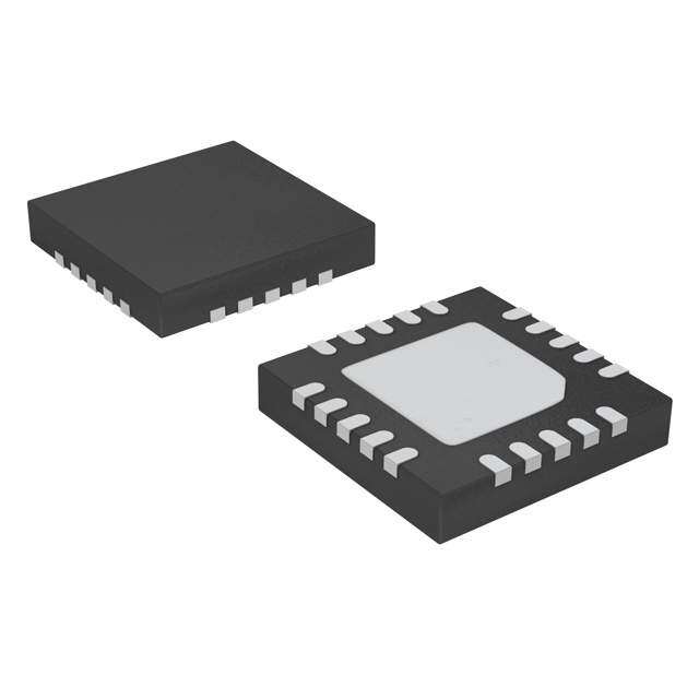
| 产品图片 |
|
| rohs | 符合RoHS无铅 / 符合限制有害物质指令(RoHS)规范要求 |
| 产品系列 | 接口 IC,LVDS 接口集成电路,Texas Instruments SN65LVDT100DGK- |
| 数据手册 | |
| 产品型号 | SN65LVDT100DGK |
| Tx/Rx类型 | LVPECL/CML/LVDS |
| 产品目录页面 | |
| 产品种类 | LVDS 接口集成电路 |
| 传播延迟时间 | 0.8 ns |
| 供应商器件封装 | 8-VSSOP |
| 其它名称 | 296-15390-5 |
| 包装 | 管件 |
| 单位重量 | 19 mg |
| 商标 | Texas Instruments |
| 安装类型 | 表面贴装 |
| 安装风格 | SMD/SMT |
| 封装 | Tube |
| 封装/外壳 | 8-TSSOP,8-MSOP(0.118",3.00mm 宽) |
| 封装/箱体 | VSSOP-8 |
| 工作温度 | -40°C ~ 85°C |
| 工作电源电压 | 3.3 V |
| 工厂包装数量 | 80 |
| 应用 | - |
| 延迟时间 | 470ps |
| 接收机数量 | 1 Receiver |
| 数据速率 | 2000 Mb/s |
| 数据速率(最大值) | 2Gbps |
| 最大工作温度 | + 85 C |
| 最小工作温度 | - 40 C |
| 标准包装 | 80 |
| 激励器数量 | 1 Driver |
| 电压-电源 | 3 V ~ 3.6 V |
| 电容-输入 | 0.6pF |
| 电流-电源 | 25mA |
| 电源电压-最大 | 3.6 V |
| 电源电压-最小 | 3 V |
| 类型 | 缓冲器, 转接驱动器 |
| 系列 | SN65LVDT100 |
| 输入 | CML,LVDS,LVPECL |
| 输出 | LVDS |
| 输出类型 | LVDS |
| 通道数 | 1 |
| 配用 | /product-detail/zh/SN65LVDS100EVM/296-20539-ND/562136 |


- 商务部:美国ITC正式对集成电路等产品启动337调查
- 曝三星4nm工艺存在良率问题 高通将骁龙8 Gen1或转产台积电
- 太阳诱电将投资9.5亿元在常州建新厂生产MLCC 预计2023年完工
- 英特尔发布欧洲新工厂建设计划 深化IDM 2.0 战略
- 台积电先进制程称霸业界 有大客户加持明年业绩稳了
- 达到5530亿美元!SIA预计今年全球半导体销售额将创下新高
- 英特尔拟将自动驾驶子公司Mobileye上市 估值或超500亿美元
- 三星加码芯片和SET,合并消费电子和移动部门,撤换高东真等 CEO
- 三星电子宣布重大人事变动 还合并消费电子和移动部门
- 海关总署:前11个月进口集成电路产品价值2.52万亿元 增长14.8%


PDF Datasheet 数据手册内容提取
Product Sample & Technical Tools & Support & Reference Folder Buy Documents Software Community Design SN65LVDS100,SN65LVDT100,SN65LVDS101,SN65LVDT101 SLLS516E–AUGUST2002–REVISEDJULY2015 SN65LVDx10x Differential Translator/Repeater 1 Features 3 Description • DesignedforSignalingRates≥ 2Gbps The SN65LVDS100, SN65LVDT100, SN65LVDS101, 1 and SN65LVDT101 are high-speed differential • TotalJitter <65ps receivers and drivers connected as repeaters. The • Low-PowerAlternativefortheMC100EP16 receiver accepts low-voltage differential signaling • Low100-ps(Maximum)Part-to-PartSkew (LVDS), positive-emitter-coupled logic (PECL), or current-mode logic (CML) input signals at rates up to • 25mVofReceiverInputThresholdHysteresis 2 Gbps and repeats it as either an LVDS or PECL Over0-Vto4-VInputVoltageRange output signal. The signal path through the device is • InputsElectricallyCompatibleWithLVPECL, differential for low radiated emissions and minimal CML,andLVDSSignalLevels addedjitter. • 3.3-VSupplyOperation DeviceInformation(1) • LVDTIntegrates110-Ω TerminatingResistor PARTNUMBER PACKAGE BODYSIZE(NOM) • OfferedinSOICandMSOP SOIC(8) 4.90mm×3.91mm SN65LVDS100 2 Applications VSSOP(8) 3.00mm×3.00mm SOIC(8) 4.90mm×3.91mm • WirelessInfrastructure SN65LVDT100 VSSOP(8) 3.00mm×3.00mm • TelecomInfrastructure SOIC(8) 4.90mm×3.91mm • Printers SN65LVDS101 VSSOP(8) 3.00mm×3.00mm SOIC(8) 4.90mm×3.91mm SN65LVDT101 VSSOP(8) 3.00mm×3.00mm (1) For all available packages, see the orderable addendum at theendofthedatasheet. DualEyeDiagram FUNCTIONALDIAGRAM EYE PATTERN SN65LVDS100 and SN65LVDS101 8 4 2Gbps VCC VBB 223- 1 PRBS 2 A 7 Y VCC= 3.3 V 6 Z VID= 200 mV B 3 VIC= 1.2 V Vert.Scale= 200 mV/div SN65LVDT100 and SN65LVDT101 1GHz 2 A 7 110W Y 6 Z 3 B Horizontal Scale= 200 ps/div 1 An IMPORTANT NOTICE at the end of this data sheet addresses availability, warranty, changes, use in safety-critical applications, intellectualpropertymattersandotherimportantdisclaimers.UNLESSOTHERWISENOTED,thisdocumentcontainsPRODUCTION DATA.
SN65LVDS100,SN65LVDT100,SN65LVDS101,SN65LVDT101 SLLS516E–AUGUST2002–REVISEDJULY2015 www.ti.com Table of Contents 1 Features.................................................................. 1 10.2 FunctionalBlockDiagram.....................................15 2 Applications........................................................... 1 10.3 FeatureDescription...............................................15 3 Description............................................................. 1 10.4 DeviceFunctionalModes......................................20 4 RevisionHistory..................................................... 2 11 ApplicationandImplementation........................ 21 11.1 ApplicationInformation..........................................21 5 Description(Continued)........................................ 3 11.2 TypicalApplication................................................22 6 DeviceOptions....................................................... 3 12 PowerSupplyRecommendations..................... 30 7 PinConfigurationandFunctions......................... 3 13 Layout................................................................... 30 8 Specifications......................................................... 4 13.1 LayoutGuidelines.................................................30 8.1 AbsoluteMaximumRatings......................................4 13.2 LayoutExample....................................................32 8.2 ESDRatings..............................................................4 14 DeviceandDocumentationSupport................. 33 8.3 RecommendedOperatingConditions.......................4 14.1 RelatedLinks........................................................33 8.4 ThermalInformation..................................................5 14.2 CommunityResources..........................................33 8.5 ElectricalCharacteristics...........................................5 14.3 Trademarks...........................................................33 8.6 SwitchingCharacteristics..........................................6 14.4 ElectrostaticDischargeCaution............................33 8.7 TypicalCharacteristics..............................................7 14.5 Glossary................................................................33 9 ParameterMeasurementInformation................12 15 Mechanical,Packaging,andOrderable 10 DetailedDescription........................................... 15 Information........................................................... 33 10.1 Overview...............................................................15 4 Revision History ChangesfromRevisionD(December2014)toRevisionE Page • ChangedFeaturesFrom:"Over0-Vto4-VCommon-ModeRange"To:"Over0-Vto4-VInputVoltageRange"................1 ChangesfromRevisionC(June2004)toRevisionD Page • AddedPinConfigurationandFunctionssection,ESDRatingstable,FeatureDescriptionsection,DeviceFunctional Modes,ApplicationandImplementationsection,PowerSupplyRecommendationssection,Layoutsection,Device andDocumentationSupportsection,andMechanical,Packaging,andOrderableInformationsection .............................. 1 2 SubmitDocumentationFeedback Copyright©2002–2015,TexasInstrumentsIncorporated ProductFolderLinks:SN65LVDS100 SN65LVDT100 SN65LVDS101 SN65LVDT101
SN65LVDS100,SN65LVDT100,SN65LVDS101,SN65LVDT101 www.ti.com SLLS516E–AUGUST2002–REVISEDJULY2015 5 Description (Continued) The outputs of the SN65LVDS100 and SN65LVDT100 are LVDS levels as defined by TIA/EIA-644-A. The outputs of the SN65LVDS101 and SN65LVDT101 are compatible with 3.3-V PECL levels. Both drive differential transmissionlineswithnominally100-Ωcharacteristicimpedance. TheSN65LVDT100andSN65LVDT101includea110-Ω differentiallineterminationresistorforlessboardspace, fewer components, and the shortest stub length possible. They do not include the V voltage reference found in BB the SN65LVDS100 and SN65LVDS101. V provides a voltage reference of typically 1.35V below V for use in BB CC receiving single-ended input signals and is particularly useful with single-ended 3.3-V PECL inputs. When V is BB notused,itshouldbeunconnectedoropen. Alldevicesarecharacterizedforoperationfrom –40°Cto85°C. 6 Device Options ORDERABLEPARTNUMBER OUTPUT TERMINATIONRESISTOR V BB SN65LVDS100D LVDS No Yes SN65LVDS100DGK LVDS No Yes SN65LVDT100D LVDS Yes No SN65LVDT100DGK LVDS Yes No SN65LVDS101D LVPECL No Yes SN65LVDS101DGK LVPECL No Yes SN65LVDT101D LVPECL Yes No SN65LVDT101DGK LVPECL Yes No 7 Pin Configuration and Functions SN65LVDS100 and SN65LVDS101 SN65LVDT100 and SN65LVDT101 D AND DGK PACKAGE D AND DGK PACKAGE (TOP VIEW) (TOP VIEW) NC 1 8 VCC NC 1 8 VCC A 2 7 Y A 2 7 Y B 3 6 Z B 3 6 Z VBB 4 5 GND NC 4 5 GND NC = Not Connected PinFunctions PIN SN65LVDS100, SN65LVDT100, I/O DESCRIPTION NAME SN65LVDS101 SN65LVDT101 A 2 2 I Differentialnon-invertinginput B 3 3 I Differentialinvertinginput GND 5 5 — Ground NC 1 1,4 — Noconnect V 4 — O Voltagereference BB V 8 8 — Supplyvoltage CC Y 7 7 O Differentialnon-invertingoutput Z 6 6 O Differentialinvertingoutput Copyright©2002–2015,TexasInstrumentsIncorporated SubmitDocumentationFeedback 3 ProductFolderLinks:SN65LVDS100 SN65LVDT100 SN65LVDS101 SN65LVDT101
SN65LVDS100,SN65LVDT100,SN65LVDS101,SN65LVDT101 SLLS516E–AUGUST2002–REVISEDJULY2015 www.ti.com 8 Specifications 8.1 Absolute Maximum Ratings(1) overoperatingfree-airtemperaturerangeunlessotherwisenoted MIN MAX UNIT V Supplyvoltagerange(2) –0.5 4 V CC I V outputcurrent –0.5 0.5 mA BB BB V I Voltagerange,(A,B,Y,Z) 0 4.3 V V O V Differentialvoltage,|V –V |('LVDT100and'LVDT101only) 1 V ID A B (1) StressesbeyondthoselistedunderAbsoluteMaximumRatingsmaycausepermanentdamagetothedevice.Thesearestressratings only,andfunctionaloperationofthedeviceattheseoranyotherconditionsbeyondthoseindicatedunderRecommendedOperating Conditionsisnotimplied.Exposuretoabsolute-maximum-ratedconditionsforextendedperiodsmayaffectdevicereliability. (2) Allvoltagevalues,exceptdifferentialI/Obusvoltages,arewithrespecttonetworkgroundterminal. 8.2 ESD Ratings VALUE UNIT Humanbodymodel(HBM),per Pins2,3,5,6,7 ±5000 V V Electrostaticdischarge ANSI/ESDA/JEDECJS-001(1) Allpinsexcept2,3,5,6,7 ±2000 V (ESD) Charged-devicemodel(CDM),perJEDECspecificationJESD22-C101(2) ±1500 V (1) TestedinaccordancewithJEDECStandard22,TestMethodA114-A.7. (2) TestedinaccordancewithJEDECStandard22,TestMethodC101. 8.3 Recommended Operating Conditions MIN NOM MAX UNIT Supplyvoltage,V 3 3.3 3.6 V CC 'LVDS100or'LVDS101 0.1 1 Magnitudeofdifferentialinputvoltage|V | V ID 'LVDT100or'LVDT101 0.1 0.8 Inputvoltage(anycombinationofcommon-modeorinputsignals),V 0 4 V I V outputcurrent,I –400(1) 12 µA BB O(VBB) Operatingfree-airtemperature,T –40 85 °C A (1) Thealgebraicconvention,inwhichthelesspositive(morenegative)limitisdesignatedminimum,isusedinthisdatasheet. 4 SubmitDocumentationFeedback Copyright©2002–2015,TexasInstrumentsIncorporated ProductFolderLinks:SN65LVDS100 SN65LVDT100 SN65LVDS101 SN65LVDT101
SN65LVDS100,SN65LVDT100,SN65LVDS101,SN65LVDT101 www.ti.com SLLS516E–AUGUST2002–REVISEDJULY2015 8.4 Thermal Information SN65LVDS100,SN65LVDT100,SN65LVDS101, SN65LVDT101 THERMALMETRIC(1) UNIT D DGK 8PINS 8PINS R Junction-to-ambientthermalresistance 208 263 °C/W θJA Powerdissipationrating:T ≤25°C 151 377 A mW Powerdissipationrating:T ≤85°C 192 481 A (1) Formoreinformationabouttraditionalandnewthermalmetrics,seetheICPackageThermalMetricsapplicationreport,SPRA953. 8.5 Electrical Characteristics overrecommendedoperatingconditions(unlessotherwisespecified) PARAMETER TESTCONDITIONS MIN TYP(1) MAX UNIT Supplycurrent,'LVDx100 Noloadorinput 25 30 I mA CC Supplycurrent,'LVDx101 R =50Ωto1V,Noinput 50 61 L Devicepowerdissipation,'LVDx100 R =100Ω,Noinput 110 L PD Devicepowerdissipation,'LVDx101 YandZtoVCC–2Vthrough50Ω 116 142 mW Noinput Referencevoltageoutput,'LVDS100 V I =–400µAor12µA V –1.4 V –1.35 V –1.3 mV BB or'LVDS101 O CC CC CC SN65LVDS100andSN65LVDS101INPUTCHARACTERISTICS(seeFigure30) Positive-goingdifferentialinput V 100 IT+ voltagethreshold SeeFigure30andTable1 mV Negative-goingdifferentialinput V –100 IT– voltagethreshold V =0Vor2.4V I –20 20 µA I Inputcurrent Secondinputat1.2V I V =4V,Secondinputat1.2V 33 µA I V =1.5V,V =0Vor2.4V CC I –20 20 Secondinputat1.2V I Poweroffinputcurrent µA I(OFF) V =1.5V,V =4V CC I 33 Secondinputat1.2V I Inputoffsetcurrent(|I -I |) V =V ,0≤V ≤4V –6 6 µA IO IA IB IA IB IA Small-signalinputcapacitanceto C V =1.2V 0.6 pF i GND I SN65LVDT100andSN65LVDT101INPUTCHARACTERISTICS(seeFigure30) Positive-goingdifferentialinput V 100 IT+ voltagethreshold SeeFigure30andTable1 mV Negative-goingdifferentialinput V –100 IT– voltagethreshold V =0Vor2.4V,Otherinputopen –40 40 I I Inputcurrent µA I V =4V,Otherinputopen 66 I V =1.5V,V =0Vor2.4V CC I –40 40 Otherinputopen I Poweroffinputcurrent µA I(OFF) V =1.5V,V =4V CC I 66 Otherinputopen V =300mVor500mV ID 90 110 132 V =0Vor2.4V IC R Differentialinputresistance Ω (T) V =0V,V =300mVor500mV CC ID 90 110 132 V =0Vor2.4V IC Small-signaldifferentialinput C V =1.2V 0.6 pF i capacitance I (1) Typicalvaluesarewitha3.3-Vsupplyvoltageandroomtemperature Copyright©2002–2015,TexasInstrumentsIncorporated SubmitDocumentationFeedback 5 ProductFolderLinks:SN65LVDS100 SN65LVDT100 SN65LVDS101 SN65LVDT101
SN65LVDS100,SN65LVDT100,SN65LVDS101,SN65LVDT101 SLLS516E–AUGUST2002–REVISEDJULY2015 www.ti.com Electrical Characteristics (continued) overrecommendedoperatingconditions(unlessotherwisespecified) PARAMETER TESTCONDITIONS MIN TYP(1) MAX UNIT SN65LVDS100andSN65LVDT100OUTPUTCHARACTERISTICS(seeFigure30) |V | Differentialoutputvoltagemagnitude 247 340 454 OD Changeindifferentialoutputvoltage SeeFigure31 mV Δ|V | –50 50 OD magnitudebetweenlogicstates Steady-statecommon-modeoutput V 1.125 1.375 V OC(SS) voltage Changeinsteady-statecommon- ΔV modeoutputvoltagebetweenlogic SeeFigure32 –50 50 mV OC(SS) states Peak-to-peakcommon-modeoutput V 50 150 mV OC(PP) voltage I Short-circuitoutputcurrent V orV =0V –24 24 mA OS O(Y) O(Z) Differentialshort-circuitoutput I V =0V –12 12 mA OS(D) current OD SN65LVDS101andSN65LVDT101OUTPUTCHARACTERISTICS(seeFigure30) 50ΩtoV –2V,SeeFigure39 V –1.25 V –1.02 V –0.9 V CC CC CC CC V High-leveloutputvoltage OH V =3.3V,50-Ωloadto2.3V 2055 2280 2405 mV CC 50ΩtoV –2V,SeeFigure39 V –1.83 V –1.61 V –1.53 V CC CC CC CC V Low-leveloutputvoltage OL V =3.3V,50-Ωloadto2.3V 1475 1690 1775 mV CC 50-ΩloadtoV –2V,See |V | Differentialoutputvoltagemagnitude CC 475 575 750 mV OD Figure39 8.6 Switching Characteristics overrecommendedoperatingconditions(unlessotherwisenoted) PARAMETER TESTCONDITIONS MIN TYP(1) MAX UNIT Propagationdelaytime, 'LVDx100 300 470 800 t ps PLH low-to-high-leveloutput 'LVDx101 400 630 900 Propagationdelaytime, 'LVDx100 300 470 800 t ps PHL high-to-low-leveloutput 'LVDx100 400 630 900 SeeFigure33 Differentialoutputsignalrisetime t 220 ps r (20%to80%) Differentialoutputsignalfalltime t 220 ps f (20%to80%) t Pulseskew(|t –t |)(2) 5 50 ps sk(p) PHL PLH t Part-to-partskew(3) V =0.2V,SeeFigure33 100 ps sk(pp) ID t RMSperiodjitter(4) 1GHz50%duty-cyclesquare-wave 1 3.7 ps jit(per) input tjit(cc) Peakcycle-to-cyclejitter(5) VID=200mV,VIC=1.2V 6 23 ps SeeFigure34 2GHzPRBS,223–1runlength t Peak-to-peakjitter V =200mV,V =1.2V 28 65 ps jit(pp) ID IC SeeFigure34 2GHzPRBS,27–1runlength t Peak-to-peakdeterministicjitter(6) V =200mV,V =1.2V 17 48 ps jit(det) ID IC SeeFigure34 (1) Alltypicalvaluesareat25°Candwitha3.3-Vsupply. (2) t isthemagnitudeofthetimedifferencebetweenthet andt ofanyoutputofasingledevice. sk(p) PLH PHL (3) t isthemagnitudeofthetimedifferenceinpropagationdelaytimebetweenanyspecifiedterminalsoftwodeviceswhenboth sk(pp) devicesoperatewiththesamesupplyvoltages,atthesametemperature,andhaveidenticalpackagesandtestcircuits. (4) Periodjitteristhedeviationincycletimeofasignalwithrespecttotheidealperiodoverarandomsampleof1,000,000cycles. (5) Cycle-to-cyclejitteristhevariationincycletimeofasignalbetweenadjacentcycles,overarandomsampleof1,000adjacentcycle pairs. (6) Deterministicjitteristhesumofpattern-dependentjitterandpulse-widthdistortion. 6 SubmitDocumentationFeedback Copyright©2002–2015,TexasInstrumentsIncorporated ProductFolderLinks:SN65LVDS100 SN65LVDT100 SN65LVDS101 SN65LVDT101
SN65LVDS100,SN65LVDT100,SN65LVDS101,SN65LVDT101 www.ti.com SLLS516E–AUGUST2002–REVISEDJULY2015 8.7 Typical Characteristics 55 60 LVDS101=Loaded LVDS101=Loaded mA 45 VTACC==253°.C3V mA 50 ent - VVICID==1.220V0mV ent - 40 VVCICC==13.2.3VV urr 35 urr VID=200mV y C y C f=750MHz pl pl 30 up up LVDS100 S LVDS100 S - C 25 - C C C 20 I I 15 10 0 200 400 600 800 1000 1200 -40 -20 0 20 40 60 80 100 Frequency - MHz TA- Free-Air Temperature -°C Figure1.SupplyCurrentvsFrequency Figure2.SupplyCurrentvsFree-AirTemperature 700 600 VCC=3.3V age - mV 600 LVDS101 me - ps 550 TfA=VID=1520=5°M2C0H0zmV tPHL oltOutput V 500 LVDS100 on Delay Ti 455000 tPLH erential 400 VCC=3.3V opagati 400 - Diff 300 TVAIC==215.°2CV - Prd 350 OD VID=200mV tp V 200 300 0 200 400 600 800 1000 1200 0 1 2 3 4 5 f - Frequency - MHz VIC- Common-Mode Input Voltage - V Figure3.DifferentialOutputVoltagevsFrequency Figure4.SN65LVDS100PropagationDelayTimevs Common-ModeInputVoltage 750 550 VCC=3.3V VCC=3.3V TA=25°C VID=200mV e - ps 700 f=VID150=M20H0zmV tPHL e - ps 500 f=150MHz tPLH m m Ti 650 Ti ay tPLH ay n Del 600 n Del 450 tPHL o o ati ati ag 550 ag p p Pro Pro 400 - 500 - d d p p t t 450 350 0 1 2 3 4 5 -40 -20 0 20 40 60 80 100 VIC- Common-Mode Input Voltage - V TA- Free-Air Temperature -°C Figure5.SN65LVDS101PropagationDelayTimevs Figure6.SN65LVDS100PropagationDelayTimevsFree-Air Common-ModeInputVoltage Temperature Copyright©2002–2015,TexasInstrumentsIncorporated SubmitDocumentationFeedback 7 ProductFolderLinks:SN65LVDS100 SN65LVDT100 SN65LVDS101 SN65LVDT101
SN65LVDS100,SN65LVDT100,SN65LVDS101,SN65LVDT101 SLLS516E–AUGUST2002–REVISEDJULY2015 www.ti.com Typical Characteristics (continued) 750 30 VCC=3.3V VCC=3.3V e - ps 700 fV=ID150=M20H0zmV 25 TVAIC==2450°C0mV m s Input=Clock ay Ti 650 tPLH er - p 20 Del Jitt on 600 tPHL ak 15 ati Pe VID=0.3V g o- opa 550 k-T 10 VID=0.5V - Pr Pea VID=0.8V d 500 5 p t 450 0 -40 -20 0 20 40 60 80 100 200 400 600 800 1000 TA- Free-Air Temperature -°C f - Frequency - MHz Figure7.SN65LVDS101PropagationDelayTimevsFree-Air Figure8.SN65LVDS100Peak-to-PeakJittervsFrequency Temperature 60 30 VOC=3.3V VCC=3.3V TA=25°C TA=25°C 50 VIC=400mV 25 VIC=400mV s Input=PRBS 223-1 s Input=Clock p p er - 40 er - 20 Jitt Jitt ak 30 ak 15 ko-Pe-T 20 VID=0.3V k-o-PeT 10 VID=0.3V VID=0.8V a a e e P P 10 VID=0.8V 5 VID=0.5V VID=0.5V 0 0 300 800 1300 1800 2300 200 400 600 800 1000 Data Rate - Mbps f - Frequency - MHz Figure9.SN65LVDS100Peak-to-PeakJittervsDataRate Figure10.SN65LVDS101Peak-to-PeakJittervsFrequency 60 30 VCC=3.3V VCC=3.3V TA=25°C TA=25°C 50 VIC=400mV 25 VIC=1.2V s Input=PRBS 223-1 s Input=Clock p p Jitter - 40 VID=0.8V VID=0.5V Jitter - 20 ak 30 ak 15 e e o-P o-P VID=0.8V k-T 20 k-T 10 VID=0.5V a a Pe Pe VID=0.3V 10 5 VID=0.3V 0 0 300 800 1300 1800 2300 200 400 600 800 1000 Data Rate - Mbps f - Frequency - MHz Figure11.SN65LVDS101Peak-to-PeakJittervsDataRate Figure12.SN65LVDS100Peak-to-PeakJittervsFrequency 8 SubmitDocumentationFeedback Copyright©2002–2015,TexasInstrumentsIncorporated ProductFolderLinks:SN65LVDS100 SN65LVDT100 SN65LVDS101 SN65LVDT101
SN65LVDS100,SN65LVDT100,SN65LVDS101,SN65LVDT101 www.ti.com SLLS516E–AUGUST2002–REVISEDJULY2015 Typical Characteristics (continued) 60 30 VCC=3.3V VCC=3.3V TA=25°C TA=25°C 50 VIC=1.2V 25 VIC=1.2V ps Input=PRBS 223-1 VID=0.3V ps Input=Clock Jitter - 40 VID=0.8V Jitter - 20 ak 30 VID=0.5V ak 15 e e P P ako--T 20 o-ak-T 10 VID=0.3V VID=0.5VVID=0.8V e e P P 10 5 0 0 300 800 1300 1800 2300 200 400 600 800 1000 Data Rate - Mbps f - Frequency - MHz Figure13.SN65LVDS100Peak-to-PeakJittervsDataRate Figure14.SN65LVDS101Peak-to-PeakJittervsFrequency 60 30 VCC=3.3V TA=25°C VCC=3.3V 50 VIC=1.2V 25 TA=25°C Input=PRBS 223-1 VIC=2.9V ps VID=0.8V ps Input=Clock er - 40 er - 20 Jitt VID=0.5V Jitt k 30 k 15 a a Pe Pe VID=0.8V o- o- VID=0.5V k-T 20 k-T 10 a a e e P P 10 5 VID=0.3V VID=0.3V 0 0 300 800 1300 1800 2300 200 400 600 800 1000 Data Rate - Mbps f - Frequency - MHz Figure15.SN65LVDS101Peak-to-PeakJittervsDataRate Figure16.SN65LVDS100Peak-to-PeakJittervsFrequency 60 30 VCC=3.3V VCC=3.3V 50 TA=25°C 25 TA=25°C VIC=2.9V VIC=2.9V Peako-Pe-Tak Jitter - ps 234000 InVpIDut==0P.8RVBS 22V3-ID1=0.3V Peak-o-PeaTk Jitter - ps 112050 IVnIpDu=t=0.C8loVck VID=0.5V 10 5 0 VID=0.5V 0 VID=0.3V 300 800 1300 1800 2300 200 400 600 800 1000 Data Rate - Mbps f - Frequency - MHz Figure17.SN65LVDS100Peak-to-PeakJittervsDataRate Figure18.SN65LVDS101Peak-to-PeakJittervsFrequency Copyright©2002–2015,TexasInstrumentsIncorporated SubmitDocumentationFeedback 9 ProductFolderLinks:SN65LVDS100 SN65LVDT100 SN65LVDS101 SN65LVDT101
SN65LVDS100,SN65LVDT100,SN65LVDS101,SN65LVDT101 SLLS516E–AUGUST2002–REVISEDJULY2015 www.ti.com Typical Characteristics (continued) 60 50 VCC=3.3V VIC=1.2V 50 k Jitter - ps 3400 VID=0.5VVID=0.3V eak Jitter - ps 3400 InVpIDut==220G0bmpsV223-1 LVDS100 a P ak-To-Pe 20 VCC=3.3V VID=0.8V Peak-To- 20 LVDS101 e P TA=25°C 10 10 VIC=2.9V Input=PRBS 223-1 0 0 300 800 1300 1800 2300 -40 -20 0 20 40 60 80 100 Data Rate - Mbps TA- Free-Air Temperature -°C Figure19.SN65LVDS101Peak-to-PeakJittervsDataRate Figure20.SN65LVDS100Peak-to-PeakJittervsFree-Air Temperature 400 80 100 VCC=3.3V, mV350 70 VIC=1.2V, Differeoltage - ntial Output V112230505000000 VV|TIVnACIpCIDC=u|=t=2==153.2°C2.C03l0Vo,V,cm,kV, 2345600000 Period Jitter - ps Peak-to-Peak Jitter - ps 24680000 |TIVnApID=u|t2==52°PC0R0,BmSV2,23-1 - D 50 10 O AddedRandomJitter V 0 0 00 1000 2000 3000 4000 0 500 1000 1500 2000 2500 Data Rate - Mbps f - Frequency - MHz Figure22.SN65LVDS100Peak-to-PeakJittervsDataRate Figure21.SN65LVDS100DifferentialOutputVoltagevs Frequency 700 50 100 VCC=3.3V, VCC=3.3V, mV VIC=1.2V, VIC=1.2V, ge - 620 |TVAID=|2=52°C00, mV, 40 s 80 |TVAID=|2=52°C00, mV, oltaOutput V 540 Input=Clock 30 Jitter - ps eak Jitter - p 60 Input=PRBS223-1 erential 460 20 Period eak-to-P 40 Diff 380 10 P 20 - OD AddedRandomJitter V 300 0 0 0 400 800 1200 1600 2000 0 1000 2000 3000 4000 5000 f - Frequency - MHz Data Rate - Mbps Figure23.SN65LVDS101DifferentialOutputVoltagevs Figure24.SN65LVDS101Peak-to-PeakJittervsDataRate Frequency 10 SubmitDocumentationFeedback Copyright©2002–2015,TexasInstrumentsIncorporated ProductFolderLinks:SN65LVDS100 SN65LVDT100 SN65LVDS101 SN65LVDT101
SN65LVDS100,SN65LVDT100,SN65LVDS101,SN65LVDT101 www.ti.com SLLS516E–AUGUST2002–REVISEDJULY2015 Typical Characteristics (continued) Horizontal Scale= 200 ps/div Horizontal Scale= 100 ps/div LVPECL-to-LVDS LVPECL-to-LVDS Figure25.SN65LVDS100Mbps,223–1PRBS Figure26.SN65LVDS100Gbps,223–1PRBS Horizontal Scale= 200 ps/div Horizontal Scale= 100 ps/div LVDS-to-LVPECL LVDS-to-LVPECL Figure27.SN65LVDS101Mbps,223–1PRBS Figure28.SN65LVDS101Gbps,223–1PRBS 20 3.6 V, 85°C 3 V, 85°C 15 mV 10 3.6 V, -40°C VIT+ d - ol 5 h s 3 V, -40°C e hr oltage T -50 3 V, -40°C |RNVoLO m=D |i1 n=0a 02l 5PW0r, omcVe,ss V ut np -10 3.6 V, -40°C VIT- I -15 3.6 V, 85°C 3 V, 85°C -20 0 1 2 3 4 5 Common-Mode Input Voltage - V V isasteady-stateparameter.Theswitchingtimeisinfluencedbytheinputoverdriveabovethissteady-statethresholduptoadifferential IT inputvoltagemagnitudeof100mV. Figure29.SN65LVDS100SimulatedInputVoltageThresholdvsCommon-ModeInputVoltage,SupplyVoltage,and Temperature Copyright©2002–2015,TexasInstrumentsIncorporated SubmitDocumentationFeedback 11 ProductFolderLinks:SN65LVDS100 SN65LVDT100 SN65LVDS101 SN65LVDT101
SN65LVDS100,SN65LVDT100,SN65LVDS101,SN65LVDT101 SLLS516E–AUGUST2002–REVISEDJULY2015 www.ti.com 9 Parameter Measurement Information IIA A Y VID B Z VOD VBB IO VIC VIA VO(Y) + VIA+2VIB VIB IIB VO(Z) VOC VB-B Figure30. VoltageandCurrentDefinitions Table1.ReceiverInputVoltageThresholdTest RESULTINGDIFFERENTIAL RESULTINGCOMMON- APPLIEDVOLTAGES INPUTVOLTAGE MODEINPUTVOLTAGE OUTPUT(1) V V V V IA IB ID IC 1.25V 1.15V 100mV 1.2V H 1.15V 1.25V –100mV 1.2V L 4.0V 3.9V 100mV 3.95V H 3.9V 4.0V –100mV 3.95V L 0.1V 0.0V 100mV 0.05V H 0.0V 0.1V –100mV 0.05V L 1.7V 0.7V 1000mV 1.2V H 0.7V 1.7V –1000mV 1.2V L 4.0V 3.0V 1000mV 3.5V H 3.0V 4.0V –1000mV 3.5V L 1.0V 0.0V 1000mV 0.5V H 0.0V 1.0V –1000mV 0.5V L (1) H=highlevel,L=lowlevel 3.74 kW Y VOD 100 W _+ 0 V ≤ V(test) ≤ 2.4 V Z 3.74 kW Figure31. SN65LVDx100DifferentialOutputVoltage(V )TestCircuit OD A 1.4 V 49.9 W ±1% A Y B 1.0 V VID VOC(PP) VOC(SS) B Z 1 pF VOC 49.9 W ±1% VOC NOTE: Allinputpulsesaresuppliedbyageneratorhavingthefollowingcharacteristics:t ort ≤0.25ns,pulserepetitionrate r f (PRR)=0.5Mpps,pulsewidth=500±10ns.C includesinstrumentationandfixturecapacitancewithin0.06mmof L thedeviceundertest.ThemeasurementofV ismadeontestequipmentwitha–3dBbandwidthofatleast300 OC(PP) MHz. Figure32. TestCircuitandDefinitionsfortheSN65LVDx100DriverCommon-ModeOutputVoltage 12 SubmitDocumentationFeedback Copyright©2002–2015,TexasInstrumentsIncorporated ProductFolderLinks:SN65LVDS100 SN65LVDT100 SN65LVDS101 SN65LVDT101
SN65LVDS100,SN65LVDT100,SN65LVDS101,SN65LVDT101 www.ti.com SLLS516E–AUGUST2002–REVISEDJULY2015 A Y VIA 1.4 V VID 1 pF VOD 100W VIA B Z VIB 1 V VIB 0.4 V VID 0 V -0.4 V VOD 50W tPHL tPLH 100% OR 50W 80% 0 V VOD 20% 0% +- VCC- 2V tf tr NOTE: Allinputpulsesaresuppliedbyageneratorhavingthefollowingcharacteristics:t ort ≤0.25ns,pulserepetitionrate r f (PRR)=50Mpps,pulsewidth=10±0.2ns.C includesinstrumentationandfixturecapacitancewithin0.06mmof L thedeviceundertest.Measurementequipmentprovidesabandwidthof5GHzminimum. Figure33. TimingTestCircuitandWaveforms CLOCK INPUT IDEALOUTPUT 0 V 0 V 1/fo 1/fo Period Jitter Cycle to Cycle Jitter ACTUALOUTPUT ACTUALOUTPUT 0 V 0 V tc(n) tc(n) tc(n+1) tjit(per)= |tc(n)- 1/fo| tjit(cc)= |tc(n)- tc(n+1)| PRBS INPUT PRBS OUTPUT 0 V 0 V tjit(pp) Figure34. DriverJitterMeasurementWaveforms Copyright©2002–2015,TexasInstrumentsIncorporated SubmitDocumentationFeedback 13 ProductFolderLinks:SN65LVDS100 SN65LVDT100 SN65LVDS101 SN65LVDT101
SN65LVDS100,SN65LVDT100,SN65LVDS101,SN65LVDT101 SLLS516E–AUGUST2002–REVISEDJULY2015 www.ti.com Power Supply 1 + 3.3V - Power Supply 2 + 1.22V - J3 J2 J1 DUT EVM VCC GND GND J4 J6 100 J5 J7 50 50 Agilent DUT E4862B Matched Matched Pattern Generator Cables Cables (NoteA) SMAto SMA SMAto SMA Tektronix EVM TDS6604 Oscilloscope (Note B) A. Sourcejitterissubtractedfromthemeasuredvalues. B. TDSJIT3jitteranalysissoftwareinstalled Figure35. JitterSetupConnectionsforSN65LVDS100andSN65LVDS101 14 SubmitDocumentationFeedback Copyright©2002–2015,TexasInstrumentsIncorporated ProductFolderLinks:SN65LVDS100 SN65LVDT100 SN65LVDS101 SN65LVDT101
SN65LVDS100,SN65LVDT100,SN65LVDS101,SN65LVDT101 www.ti.com SLLS516E–AUGUST2002–REVISEDJULY2015 10 Detailed Description 10.1 Overview The SN65LVDx10x family of devices are fully differential, high-speed translators/repeaters. All devices in the family include a wide common-mode range receiver that accepts low-voltage differential signals covering a variety of standards. A receiver with an input sensitivity of ±100 mV and 25 mV of hysteresis is incorporated. The SN65LVDx100 devices include an output driver that meets all the specifications of the LVDS standard (TIA/EIA- 644A).TheSN65LVDx101devicesincludeanoutputdriverthatiscompatiblewith3.3-VPECLlevels. TheSN65LVDx10xfamilyisintendedtodrivea100-Ω transmissionline.Thistransmissionlinemaybeaprinted- circuit board (PCB) or cabled interconnect. With transmission lines, optimum signal quality and power delivery is reached when a transmission line is terminated with a load equal to the characteristic impedance of the interconnecting media. Likewise, the driven 100-Ω transmission line should be terminated with a matched resistance. 10.2 Functional Block Diagram SN65LVDS100 and SN65LVDS101 8 4 V V CC BB 2 A 7 Y 6 Z 3 B SN65LVDT100 and SN65LVDT101 2 A 7 Y 110W 6 Z 3 B 10.3 Feature Description 10.3.1 ReceiverFeatures 10.3.1.1 VoltageRangeandCommon-ModeRange The receiver circuit incorporated into the SN65LVDx10x family supports receiving most low-voltage differential signals. This wide common-mode range receiver can accept any input signal between 0 and 4 V. Without referencing any specific standard, we can analyze the range of signals that can be input to this family of devices. Assuming an input signal has a 400-mV differential input voltage |(V+ – V–)|, the maximum recommended input voltageis4V.TheabsolutevalueofthemostpositivesignalofadifferentialinputwouldbeV : MAX V =V +½(V ) MAX CM DIFF where • V =common-modevoltage CM • V =differentialvoltage (1) DIFF Therefore, using our V of 4 V and V of 400 mV, we see that we can simultaneously support a differential MAX DIFF voltage of 400 mV and a common-mode voltage of 3.8 V. As is obvious from Equation 1, the common-mode and differential voltages are coupled: as the differential voltage increases in magnitude, the maximum common-mode voltagesupporteddecreases. Using a similar analysis, and considering the 0-V minimum input voltage, we can see that we could simultaneously support a differential voltage of 400 mV and a common-mode voltage of 0.2 V. Thus, we have a receiverthatcansupportcommon-modevoltagesintheapproximaterangeof0.2Vto3.8V. Copyright©2002–2015,TexasInstrumentsIncorporated SubmitDocumentationFeedback 15 ProductFolderLinks:SN65LVDS100 SN65LVDT100 SN65LVDS101 SN65LVDT101
SN65LVDS100,SN65LVDT100,SN65LVDS101,SN65LVDT101 SLLS516E–AUGUST2002–REVISEDJULY2015 www.ti.com Feature Description (continued) The 400-mV example alluded to above is a reasonable maximum differential input voltage across a wide variety of standards (LVDS, M-LVDS, CML, LVPECL, and so on). We can use the specifications for any of these standardstounderstandthevalueofthiswideinputrangereceiver. A standard compliant LVDS driver generates a 350-mV differential signal with a common-mode voltage of 1.2 V. Thenoninvertingoutputthusresidesat1.375V,whiletheinvertingsignalisatavoltageof1.025V.Becausethe SN65LVDx10x family receiver operates over a range of 0 V to 4 V, the wide common-mode receiver then can accept signals that are common-mode shifted by –1.025 V to 2.625 V. Similar analysis can be performed for any otherinputsignal. 10.3.1.2 Sensitivity Table 2 provides a truth table for the SN65LVDx10x family. Again, the same receiver circuitry is used on each of the devices in this family; therefore, the truth table is the same for all family devices. When the differential input voltage is greater than 100 mV, the receiver outputs a HI level. If the differential input voltage is less than –100 mV,thereceiveroutputsaLOlevel. Between these two thresholds the receiver output is indeterminate. When the input signal falls in this –100 mV < V < 100 mV range, the receiver output state cannot be determined unambiguously. Having said that, it is ID important to note that the SN65LVDx10x family receivers include 25 mV of hysteresis. The hysteresis is incorporated into the design to prevent the output switching when the receiver input voltage is close to 0 V (for example, the receiver inputs are open-circuited, or the receiver is connected to a driver that is high-impedance). With the open-circuited input and when the magnitude of the differential noise voltage on the bus is low (approximately < ±10 mV), the hysteresis serves to hold the device output at the last known state. This feature helpspreventchatteringonthedeviceoutput. Noticeably absent from this receiver is any integrated failsafe feature. External components may be added to the receivercircuittoprovidefailsafe.Suchanimplementationiscoveredbelow. 10.3.1.3 FailsafeConsiderations Failsafe, in regard to a line receiver, usually means that the output goes to a defined logical state with no input signal. To keep added jitter to an absolute minimum, the SN65LVDS100 does not include this feature. It does exhibit 25 mV of input voltage hysteresis to prevent oscillation and keep the output in the last state prior to input- signalloss(assumingthedifferentialnoiseinthesystemislessthanthehysteresis). Should failsafe be required, it may be added externally with a 1.6-kΩ pullup resistor to the 3.3-V supply and a 1.6-kΩ pulldown resistor to ground as shown in Figure 36 The default output state is determined by which line is pulled up or down and is the user's choice. The location of the 1.6-kΩ resistors is not critical. However, the 100- Ωresistorshouldbelocatedattheendofthetransmissionline. 3.3 V 1.6 kW 100 W 1.6 kW Figure36. ExternalFailsafeCircuit Addition of this external failsafe will reduce the differential noise margin and add jitter to the output signal. The roughly 100-mV steady-state voltage generated across the 100-Ω resistor adds (or subtracts) from the signal generated by the upstream line driver. If the differential output of the line driver is symmetrical about zero volts, then the input at the receiver will appear asymmetrical with the external failsafe. Perhaps more important, is the extratimeittakesfortheinputsignaltoovercometheaddedfailsafeoffsetvoltage. 16 SubmitDocumentationFeedback Copyright©2002–2015,TexasInstrumentsIncorporated ProductFolderLinks:SN65LVDS100 SN65LVDT100 SN65LVDS101 SN65LVDT101
SN65LVDS100,SN65LVDT100,SN65LVDS101,SN65LVDT101 www.ti.com SLLS516E–AUGUST2002–REVISEDJULY2015 Feature Description (continued) In Figure 37 and using an external failsafe, the high-level differential voltage at the input of the SN65LVDS100 reaches 340 mV and the low-level –400 mV indicating a 60-mV differential offset induced by the external failsafe circuitry. The figure also reveals that the lowest peak-to-peak time jitter does not occur at zero-volt differential (thenominalinputthresholdofthereceiver)butat –60mV,thefailsafeoffset. The added jitter from external failsafe increases as the signal transition times are slowed by cable effects. When aten-meterCAT-5UTPcableisintroducedbetweenthedriverandreceiver,thezero-crossingpeak-to-peakjitter at the receiver output adds 250 ps when the external failsafe is added with this specific test set up. If external failsafeisusedinconjunctionwiththeSN65LVDS100,thenoisemarginandjittereffectsshouldbebudgeted. Figure37. ReceiverInputEyePatternwithExternalFailsafe 10.3.1.4 V VoltageReference BB Pin 4 (V ) on the SN65LVDS10x devices acts a voltage reference. This is an output signal from the device, with BB a nominal value of V – 1.35 V. This output can be used when receiving a single-ended input signal. This CC voltage reference would then be connected to the inverting input pin on the device (pin 3: B). The application where such a use makes sense is when the device is to receive a single-ended 3.3-V LVPECL signal. The common-mode voltage of a 3.3-V LVPECL signal is approximately 1.35 V below the device supply rail. While the value of V is ideal for single-ended LVPECL signals, its use may be extended to other single-ended inputs as BB long as the active single-ended signal is conditioned to have a common-mode voltage close to the nominal value ofV . BB Caution is in order when using the V signal. The expected application when using this signal is as a voltage BB reference to high-impedance input. The maximum current that can be sourced by this pin is 400 μA, while the maximum current that can be sunk is 12 μA. In cases where the SN65LVDS10x device is to be used without usingV asareference,theV pinshouldbeleftunconnected. BB BB 10.3.1.5 IntegratedTermination The SN65LVDT10x devices are identical to the SN65LVDS10x devices in all regards, with the addition that the SN65LVDT10x devices incorporate an integrated termination resistor along with the receiver. This termination would take the place of the matched load-line termination mentioned above. The SN65LVDT10x can be used in a point-to-point system or in a multidrop system when it is the last receiver on the multidrop bus. The SN65LVDT10x should not be used at every node in a multidrop system as this would change the loaded bus impedancethroughoutthebusresultinginmultiplereflectionsandsignaldistortion. Copyright©2002–2015,TexasInstrumentsIncorporated SubmitDocumentationFeedback 17 ProductFolderLinks:SN65LVDS100 SN65LVDT100 SN65LVDS101 SN65LVDT101
SN65LVDS100,SN65LVDT100,SN65LVDS101,SN65LVDT101 SLLS516E–AUGUST2002–REVISEDJULY2015 www.ti.com 10.3.1.6 ReceiverEquivalentSchematic The SN65LVDx10x equivalent input schematic diagram is shown in Figure 38. The receiver input is a high- impedance differential pair in the case of the SN65LVDS10x. The SN65LVDT10x devices include an internal termination resistor of 110 Ω across the input port. 7-V Zener diodes are included on each input to provide ESD protection. INPUT VCC A B VCC VCC 110 VCC (SN65LVDT only) 215 A 215 A 7 V 7 V 350 A 350 A Figure38. ReceiverEquivalentSchematic 10.3.2 DriverFeatures 10.3.2.1 SignalingRate,EdgeRate,andAddedJitter The SN65LVDT10x family has been designed to provide uncompromising signal quality at signaling rates up to 2 Gbps, and beyond. Specifying a maximum signaling rate (the signaling rate is the same as the bit rate) for a device depends on the eye quality that can be achieved. This eye quality is driven by a number of factors, with twoofthemostcriticalparametersbeingtheriseorfalltimeandaddedjitter. The rise and fall times for a device are critical for an obvious reason: the time it takes for a device to change states will be a limiting factor in how fast a device can be operated. If a device is operated much faster than the speed at which it can change states, the vertical opening of the eye diagram will be decreased. In some cases this may be perfectly acceptable. As an example, assume an SN65LVDS100 is being using to receive a CML signal, and translate the CML signal into an LVDS signal. At speeds up to 2 Gbps (or 1 GHz for a clock signal because there are 2 bit times for each clock cycle), the LVDS output signal will have a differential output voltage of at least 247 mV, with a nominal value of 340 mV (see the Electrical Characteristics section for reference). If the input is at a higher speed, there is no circuitry within the SN65LVDS100 that would prevent the device from trying to output an LVDS signal. As the signaling rate is increased beyond 2 Gbps, the output signal would show a decrease in vertical eye opening. This decrease may not impact the utility of the device at the system level. Signal chain noise analysis would need to be performed to determine whether the overall system would be affected. In a similar way, we can see the effect of added jitter, and how it can place upper limits on the useful operating rate. At the stated 2-Gbps signaling rate, the unit interval (UI) time, t , is the reciprocal of 2 Gbps, or 500 ps. As UI added jitter is introduced by a device such as the SN65LVDT10x family, it serves to close down the eye pattern horizontally (or in time). As the output eye diagram will eventually be used to recover the transmitted or encoded data, the jitter tolerance at the eventual consumer would determine if the eye closure introduced by a SN65LVDT10x is acceptable. The nominal total jitter for the SN65LVDT10x family devices is 28 ps, while the worst case jitter is 65 ps. The 28 ps represents less than 6% of the UI and the 65 ps represents 13% of the UI. Bothvalueswillgenerallybewithintheamountofaddedjitterthatcanbetoleratedinasystem. 10.3.2.2 SN65LVDx100LVDSOutput 10.3.2.2.1 DriverOutputVoltage The SN65LVDx100 driver operates and meets all the specified performance requirements for supply voltages in the range of 3 V to 3.6 V. The driver output voltage has a nominal value of 340 mV, with maximum and minimum outputvoltagesthatmeettheLVDSstandardspecificationsof247mVand454mV,respectively. 18 SubmitDocumentationFeedback Copyright©2002–2015,TexasInstrumentsIncorporated ProductFolderLinks:SN65LVDS100 SN65LVDT100 SN65LVDS101 SN65LVDT101
SN65LVDS100,SN65LVDT100,SN65LVDS101,SN65LVDT101 www.ti.com SLLS516E–AUGUST2002–REVISEDJULY2015 10.3.2.2.2 DriverOffset An LVDS compliant driver is required to maintain the common-mode output voltage at 1.2 V (±75 mV). The SN65LVDx100 incorporates sense circuitry and a control loop to source common-mode current and keep the output signal within specified values. Further, the device maintains the output common-mode voltage at this set pointoverthefull3-Vto3.6-Vsupplyrange. 10.3.2.3 SN65LVDx101LVPECLOutput 10.3.2.3.1 DriverVoltage The SN65LVDx101 driver is an LVPECL differential driver. Figure 40 shows an equivalent output schematic for the SN65LVDx101 driver. The differential signal output of the driver is simply the output of the differential pair, emitter-coupled to the device output. For an ECL class device such as this, the output base-emitter diodes must always be on. This need for the consistently active output stages helps explain the classical ECL load shown in Figure39. VOY + 50 W VOD - VOZ 50 W +- VCC - 2V Figure39. TypicalTerminationforLVPECLOutputDriver(SN65LVDx101) Figure 39 shows that the SN65LVDx101 outputs drive 50-Ω loads terminated to a supply that is 2 V below the supply voltage of the SN65LVDx101 device. Driving a load that is referenced to a supply 2 V below the device supply assures that the final transistor stages in the output driver are always on. A common question for those new to ECL devices concerns the implementation of this output load. There is no need generally to have a regulated supply to support this. A Thevenin load is often used to create a 50-Ω effective termination, at a common-mode voltage 2 V below the local supply rail. Many other implementations have been used. The key to the specific load that is implemented lies in the understanding that the ECL driver output stage is a voltage driver, with the output voltage always referenced to the positive power rail for the device. The load that is driven mustensurethatthefinaltransistorsoneachoutputlegareintheactiveregionsatalltimes. 10.3.2.4 DriverEquivalentSchematics The SN65LVDx10x equivalent output schematic diagrams are shown in Figure 40. The SN65LVDx10x output is represented by a differential pair with 7-V Zener diodes on each output leg. The Zener diodes provide ESD protection. The SN65LVDx10x1 LVPECL output is represented by a differential pair, with follower stages, and with7-VZenerdiodesoneachoutputlegforESDprotection. Copyright©2002–2015,TexasInstrumentsIncorporated SubmitDocumentationFeedback 19 ProductFolderLinks:SN65LVDS100 SN65LVDT100 SN65LVDS101 SN65LVDT101
SN65LVDS100,SN65LVDT100,SN65LVDS101,SN65LVDT101 SLLS516E–AUGUST2002–REVISEDJULY2015 www.ti.com OUTPUT OUTPUT (SN65LVDS100 and SN65LVDT100) (SN65LVDS101 and SN65LVDT101) VCC VCC R R R R Y Y Z VCC 7 V 7 V 7 V Z 7 V Figure40. DriverEquivalentSchematics 10.4 Device Functional Modes Table2.SN65LVDx10xTruthTable DIFFERENTIALINPUT OUTPUTS(1) V =V –V Y Z ID A B V ≥100mV H L ID –100mV<V <100mV ? ? ID V ≤–100mV L H ID Open ? ? (1) H=highlevel,L=lowlevel,?=indeterminate 20 SubmitDocumentationFeedback Copyright©2002–2015,TexasInstrumentsIncorporated ProductFolderLinks:SN65LVDS100 SN65LVDT100 SN65LVDS101 SN65LVDT101
SN65LVDS100,SN65LVDT100,SN65LVDS101,SN65LVDT101 www.ti.com SLLS516E–AUGUST2002–REVISEDJULY2015 11 Application and Implementation NOTE Information in the following applications sections is not part of the TI component specification, and TI does not warrant its accuracy or completeness. TI’s customers are responsible for determining suitability of components for their purposes. Customers should validateandtesttheirdesignimplementationtoconfirmsystemfunctionality. 11.1 Application Information The SN65LVDx10x are single-channel repeaters/translators. The functionality of these devices is simple, yet extremely flexible, leading to their use in designs ranging from wireless base stations to desktop computers. SN65LVDx10x devices are often used as buffers to regenerate or repeat the signal at their port. The devices in this family can accept any differential signal that meets the input port requirements specified herein. The input signal does not need to comply with any particular standard to be repeated: it just needs to fall within the common-mode input range of these devices, and have a differential input signal of at least 100 mV in magnitude. With such an input the designer can use a SN65LVDx100 device to repeat the digital input signal, and generate an output signal that carries the information at its input port, and complies with all the requirements of the LVDS standard.Similarly,anSN65LVDx101deviceisageneral-purposedifferentialreceiverthatrepeatstheinputdata atitsoutputport,whilecomplyingwithLVPECLoutputspecifications. Translating from one signaling standard to a different signaling standard is a common application issue. Two ICs that use different signaling standards may need to communicate with each other. An FPGA may output an LVDS signal and an ASIC may be designed to receive LVPECL inputs. Directly connecting the two devices would end up with communication errors. In such a case an SN65LVDS101 can be used to translate between the incompatible standards. The common application issue of converting from one standard to another are covered inTypicalApplication. Copyright©2002–2015,TexasInstrumentsIncorporated SubmitDocumentationFeedback 21 ProductFolderLinks:SN65LVDS100 SN65LVDT100 SN65LVDS101 SN65LVDT101
SN65LVDS100,SN65LVDT100,SN65LVDS101,SN65LVDT101 SLLS516E–AUGUST2002–REVISEDJULY2015 www.ti.com 11.2 Typical Application 11.2.1 PECLtoLVDSTranslation V CC ECL SSNN6655LLVVDDSS110000 100 V 50 50 EE V -2 V CC Figure41. PECLtoLVDSTranslation 11.2.1.1 DesignRequirements DESIGNPARAMETER EXAMPLEVALUE PECLSourceSupplyVoltage(V ) 3.3V CC SN65LVDS100SupplyVoltage 3.0to3.6V DriverSignalingRate DCto2000Mbps InterconnectCharacteristicImpedance 100Ω TerminationResistance 50ΩtoV –2Voneachsideoftransmissionline CC 11.2.1.2 DetailedDesignRequirements TranslatinganLVPECLsignaltoLVDSisstraightforwardusingtheSN65LVDS100.Thecommon-modeoutputof an LVPECL driver is approximately 2 V, while the differential output voltage would be approximately 600 to 800 mV. 2 V is right in the middle of the common-mode range of the SN65LVDS100, while the differential voltage is more than enough signal for the high-sensitivity receiver. As shown in Figure 41, 50-Ω pulldown resistors to V –2Vareneeded,andtherationaleforthesehavebeendiscussedearlier. CC 11.2.1.3 ApplicationCurve Horizontal Scale= 200 ps/div LVPECL-to-LVDS Figure42.SN65LVDS100Mbps,223–1PRBS 22 SubmitDocumentationFeedback Copyright©2002–2015,TexasInstrumentsIncorporated ProductFolderLinks:SN65LVDS100 SN65LVDT100 SN65LVDS101 SN65LVDT101
SN65LVDS100,SN65LVDT100,SN65LVDS101,SN65LVDT101 www.ti.com SLLS516E–AUGUST2002–REVISEDJULY2015 11.2.2 LVDSto3.3-VPECLTranslation LVDS SN65LVDT101 LVDS 3.3 V PECL 50Ω 50Ω 1.3 V Figure43. LVDSto3.3-VPECLTranslation 11.2.2.1 DesignRequirements DESIGNPARAMETER EXAMPLEVALUE LVDSSourceSupplyVoltage(V ) 3.3V CC SN65LVDT101SupplyVoltage 3.0to3.6V DriverSignalingRate DCto2000Mbps InterconnectCharacteristicImpedance 100Ω TerminationResistance IntegratedinSN65LVDT101 11.2.2.2 DetailedDesignRequirements Translating an LVDS signal to LVPECL is conveniently done using the SN65LVDT101. The common-mode output of an LVDS driver is 1.2 V, while the differential output voltage would be approximately 350 mV. 1.2 V is well within the common-mode range of the SN65LVDT101, while the differential voltage is more than enough signal for the high-sensitivity receiver. The integrated variant of the LVPECL translators is used here as it includespreciselytheloadrequiredforoperationofanLVDSdriver.ThiscircuitisshowninFigure43. 11.2.2.3 ApplicationCurve Horizontal Scale= 200 ps/div LVDS-to-LVPECL Figure44.SN65LVDS101Mbps,223–1PRBS Copyright©2002–2015,TexasInstrumentsIncorporated SubmitDocumentationFeedback 23 ProductFolderLinks:SN65LVDS100 SN65LVDT100 SN65LVDS101 SN65LVDT101
SN65LVDS100,SN65LVDT100,SN65LVDS101,SN65LVDT101 SLLS516E–AUGUST2002–REVISEDJULY2015 www.ti.com 11.2.3 5-VPECLto3.3-VPECLTranslation 5 V ECL SN65LVDS101 3.3 V PECL 50Ω 50Ω 50Ω 50Ω V EE 3 V 1.3 V Figure45. 5-VPECLto3.3-VPECLTranslation 11.2.3.1 DesignRequirements DESIGNPARAMETER EXAMPLEVALUE PECLSourceSupplyVoltage(V ) 5.0V CC SN65LVDS101SupplyVoltage 3.0to3.6V DriverSignalingRate DCto2000Mbps InterconnectCharacteristicImpedance 100Ω TerminationResistance 50ΩtoV –2Voneachsideoftransmissionline CC 11.2.3.2 DetailedDesignRequirements At times a 5-V PECL will need to be converted to a 3.3-V PECL signal. When the 5-V signal is encoded (8b10b forexample),ac-couplingcanbeused.Figure45showshowtotranslatea5-VPECLsignalto3.3-VPECLwhen adcconnectionisneeded. The 50-Ω pulldown resistors to V – 2 V are familiar by now. The SN65LVDS101 provides the 3.3-V based CC LVPECLsignal. A level of care must be exercised with this solution. The absolute voltage levels at the input pins to the SN65LVDS101 must be less than or equal to 4 V. With a 5-V PECL signal, the non-inverting output will generally be just below 4 V. If the 5-V PECL supply goes much above 5 V, the input voltage at the SN65LVDS101 may violate the specifications. Ensure that the worst-case high-output voltage from the 5-V PECL driver will be within therangeoftheSN65LVDS101. 11.2.3.3 ApplicationCurve Reference:Figure44 24 SubmitDocumentationFeedback Copyright©2002–2015,TexasInstrumentsIncorporated ProductFolderLinks:SN65LVDS100 SN65LVDT100 SN65LVDS101 SN65LVDT101
SN65LVDS100,SN65LVDT100,SN65LVDS101,SN65LVDT101 www.ti.com SLLS516E–AUGUST2002–REVISEDJULY2015 11.2.4 CMLtoLVDSor3.3-VPECLTranslation V TT 50 50 CML SN65LVDS100 or SN65LVDS101 Figure46. CMLtoLVDSor3.3-VPECLTranslation 11.2.4.1 DesignRequirements DESIGNPARAMETER EXAMPLEVALUE CMLTerminationSupplyVoltage(V ) 3.3V TT SN65LVDS10xSupplyVoltage 3.0to3.6V DriverSignalingRate DCto2000Mbps InterconnectCharacteristicImpedance 100Ω TerminationResistance 50ΩtoV oneachsideoftransmissionline TT 11.2.4.2 DetailedDesignRequirements Current-mode logic (CML) signals are designed to drive a 100-Ω transmission line with a load termination being two 50-Ω pullup resistors to a power supply. This circuit is shown in Figure 46. Common CML drivers include 16- mA current sources that serve to develop the differential output signal. Using this 16-mA current source and assuming a 3.3-V CML driver is being used, the common-mode output of the driver in Figure 46 is 2.9 V and the differential output voltage is 800 mV. Both values are well within the operational envelope of the SN65LVDx10x familyreceivers. To convert from 3.3-V CML signals to LVDS signals, the driver and receiver are connected in a straightforward fashion.TheSN65LVDS100isusedinthiscircuittoconverttoanLVDSoutput,whiletheSN65LVDS101isused toconverttoLVPECL. Again, the reader will notice that the integrated termination devices in the SN65LVDx10x family are not mentioned for this conversion. The ‘LVDT devices incorporate a shunt 100-Ω termination which are not appropriatewhenapullupterminationisneeded. 11.2.4.3 ApplicationCurve Reference:Figure44 Copyright©2002–2015,TexasInstrumentsIncorporated SubmitDocumentationFeedback 25 ProductFolderLinks:SN65LVDS100 SN65LVDT100 SN65LVDS101 SN65LVDT101
SN65LVDS100,SN65LVDT100,SN65LVDS101,SN65LVDT101 SLLS516E–AUGUST2002–REVISEDJULY2015 www.ti.com 11.2.5 Single-Ended3.3-VPECLtoLVDSTranslation 3.3 V ECL SN65LVDS100 Z = 50 0 100 LVDS 50 VEE 0.01 F VBB 22 k Figure47. Single-Ended3.3-VPECLtoLVDSTranslation 11.2.5.1 DesignRequirements DESIGNPARAMETER EXAMPLEVALUE ECLSupplyVoltage 3.3V SN65LVDS100SupplyVoltage 3.0to3.6V DriverSignalingRate DCto2000Mbps InterconnectCharacteristicImpedance 50Ω TerminationResistance 50ΩtoGND V CurrenttoGND 91µA BB 11.2.5.2 DetailedDesignRequirements The SN65LVDx10x family of devices provides the flexibility to translate single-ended input signals to differential outputs. The output can be either LVDS or LVPECL, depending on the choice of SN65LVDS10x that is used. Figure47demonstrateshowtoconvertasingle-endedLVPECLsignaltoanLVDSsignal. The common receiver used in this family will work with any pair of input signals that comply with its input requirements.Inthisexample,let’sassumethesingle-sidedLVPECLsignalhasahigh-levelvoltageofV – 1V CC = 2.3 V. Assume the low-level output voltage is V – 1.6 V = 1.7 V. The common-mode of these two levels is 2 CC V,whichhappenstobeV –1.3V. CC To use a single-ended signal with these receivers, we need to bias the unused input of the differential receiver. In this case we will bias the inverting input pin. With the high and low signal levels calculated above, we see the optimum bias point for the unused pin would be the common-mode or average signal level. The V pin provides BB thisneededvoltage.V hasanominalvalueofV –1.35V. BB CC The 22-kΩ resistor in the circuit serves to limit the dc current being sourced by V . This resistor setting will limit BB thecurrenttolessthan100μA,wellwithintherecommendedmaximumvalueof400 μA. Thedrawbackofasingle-endedtodifferential-convertedshownhereisthattheunusedpinisbeingsettoafixed value that will be close to the signal common-mode voltage. Any deviation from V (in the actual signal BB common-mode) results in duty-cycle distortion at the differential output. Whether or not this is an issue is application dependent. If, for example, the input signal is a clock signal and clocking only happens on one edge, thedistortionmaybeacceptable. 11.2.5.3 ApplicationCurve Reference:Figure42 26 SubmitDocumentationFeedback Copyright©2002–2015,TexasInstrumentsIncorporated ProductFolderLinks:SN65LVDS100 SN65LVDT100 SN65LVDS101 SN65LVDT101
SN65LVDS100,SN65LVDT100,SN65LVDS101,SN65LVDT101 www.ti.com SLLS516E–AUGUST2002–REVISEDJULY2015 11.2.6 Single-EndedCMOStoLVDSTranslation V DD V /600 A* 1 V < V < 4 V DD DD CMOS SN65LVDS100 100 LVDS 0.01 F V /600 A* DD *closeststandardvalue Figure48. Single-EndedCMOStoLVDSTranslation 11.2.6.1 DesignRequirements DESIGNPARAMETER EXAMPLEVALUE CMOSSupplyVoltage(V ) 1V<V <4V DD DD SN65LVDS100SupplyVoltage 3.0to3.6V DriverSignalingRate DCto500Mbps V CurrenttoGND 91µA(V =4V) BB DD 11.2.6.2 DetailedDesignRequirements The SN65LVDx10x family of devices can also translate a CMOS input signals to differential outputs. The output canbeeitherLVDSorLVPECL,dependingonthechoiceofSN65LVDS10xthatisused.Figure48 demonstrates howtoconvertaCMOSsignaltoanLVDSsignal. The CMOS signal in this case can be from any power rail up to 4 V (not a common rail, but the maximum allowable input at the receiver nonetheless). The unused or inverting signal in this case is biased to V /2 which DD willbeequaltothecommon-modeoftheCMOSinputsignal. There is less concern with this circuit with regards to duty-cycle distortion, as we have assumed that the CMOS driver and the local voltage divider are referenced to the same rail. If different rails were used, the usual cautions onduty-cycledistortionwouldapply. 11.2.6.3 ApplicationCurve Reference:Figure42 Copyright©2002–2015,TexasInstrumentsIncorporated SubmitDocumentationFeedback 27 ProductFolderLinks:SN65LVDS100 SN65LVDT100 SN65LVDS101 SN65LVDT101
SN65LVDS100,SN65LVDT100,SN65LVDS101,SN65LVDT101 SLLS516E–AUGUST2002–REVISEDJULY2015 www.ti.com 11.2.7 Single-EndedCMOSto3.3-VPECLTranslation V DD 1V < V < 4 V DD VDD/600 μA* CMOS SN65LVDS101 3.3 V PECL 50Ω 50Ω 0.01μF VDD/600μA* 1.3 V ∗closeststandard value Figure49. Single-EndedCMOSto3.3-VPECLTranslation 11.2.7.1 DesignRequirements DESIGNPARAMETER EXAMPLEVALUE CMOSSupplyVoltage(V ) 1V<V <4V DD DD SN65LVDS101SupplyVoltage 3.0to3.6V DriverSignalingRate DCto500Mbps V CurrenttoGND 91µA(V =4V) BB DD 11.2.7.2 DetailedDesignRequirements Figure 49 demonstrates how to implement a CMOS to LVPECL translation. The elements in this circuit are now familiar,sothereaderisreferredtothepreviousdiscussions. 11.2.7.3 ApplicationCurve Reference:Figure44 28 SubmitDocumentationFeedback Copyright©2002–2015,TexasInstrumentsIncorporated ProductFolderLinks:SN65LVDS100 SN65LVDT100 SN65LVDS101 SN65LVDT101
SN65LVDS100,SN65LVDT100,SN65LVDS101,SN65LVDT101 www.ti.com SLLS516E–AUGUST2002–REVISEDJULY2015 11.2.8 ReceiptofAC-CoupledSignals C SN65LVDS100 or 50 SN65LVDS101 50 C V BB 0.01 F 22 k Figure50. ReceiptofAC-CoupledSignals 11.2.8.1 DesignRequirements DESIGNPARAMETER EXAMPLEVALUE AC-couplingcapacitor 10nF SN65LVDS100SupplyVoltage 3.0to3.6V DriverSignalingRate Upto500Mbps V CurrenttoGND 91µA(V =4V) BB DD Low-FrequencyCutoffofRCFilter 318kHz 11.2.8.2 DetailedDesignRequirements The general need to convert ac-coupled signals to either LVDS or LVPECL is shown in Figure 50. The transmission line is terminated with a center-tapped 100-Ω resistor network. The center tap is tied to the previously discussed V bias reference. The bias reference is current limited with the same 22-kΩ resistor to BB ground. The use of V is chosen for ease. This sets the common-mode at the receiver input approximately in BB themiddleofthereceiverinputrange(approximately2V). The ac-coupling capacitors used on the input signal may be integrated into the source destination device, or may be discretely inserted on board. The capacitance value and the 50-Ω to ground terminations serve as a high- pass filter, blocking dc content. With a 10-nF capacitor the low-frequency zero is at 318 kHz. The reader needs tounderstandthefrequencycontentoftheincomingsignaltodeterminewhetherthiszerolocationisappropriate. 11.2.8.3 ApplicationCurve Reference:Figure42 Copyright©2002–2015,TexasInstrumentsIncorporated SubmitDocumentationFeedback 29 ProductFolderLinks:SN65LVDS100 SN65LVDT100 SN65LVDS101 SN65LVDT101
SN65LVDS100,SN65LVDT100,SN65LVDS101,SN65LVDT101 SLLS516E–AUGUST2002–REVISEDJULY2015 www.ti.com 12 Power Supply Recommendations The LVDS drivers in this data sheet are designed to operate from a single power supply, with supply voltages in the range of 3.0 V to 3.6 V. In a typical application, a driver and a receiver may be on separate boards, or even separate equipment. In these cases, separate supplies would be used at each location. The expected ground potential difference between the driver power supply and the receiver power supply would be less than |±1 V|. Boardlevelandlocaldevicelevelbypasscapacitanceshouldbeusedandhavebeencovered. 13 Layout 13.1 Layout Guidelines 13.1.1 Microstripvs.StriplineTopologies As per SLLD009, modern printed-circuit boards usually offer designers two transmission line options: Microstrip andstripline.MicrostripsaretracesontheouterlayerofaPCB,asshowninFigure51. Figure51. MicrostripTopology On the other hand, striplines are traces between two ground planes. Striplines are less prone to emissions and susceptibility problems since the reference planes effectively shield the embedded traces. However, from the standpoint of high-speed transmission, juxtaposing two planes creates additional capacitance. TI recommends routing LVDS signals on microstrip transmission lines, if possible. The PCB traces allow designers to specify the necessary tolerances for Z based on the overall noise budget and reflection allowances. Footnotes 1, 2, and 3 O provideformulasforZ andt fordifferentialandsingle-endedtraces. (1) (2) (3) O PD Figure52. StriplineTopology 13.1.2 DielectricTypeandBoardConstruction The speeds at which signals travel across the board dictates the choice of dielectric. FR-4, or equivalent, usually provides adequate performance for use with LVDS signals. If rise or fall times of TTL/CMOS signals are less than 500 ps, empirical results indicate that a material with a dielectric constant near 3.4, such as Rogers™ 4350 or Nelco N4000-13 is better suited. Once the designer chooses the dielectric, there are several parameters pertaining to the board construction that can affect performance. The following set of guidelines were developed experimentallythroughseveraldesignsinvolvingLVDSdevices: • Copperweight:15gor1/2ozstart,platedto30gor1oz • Allexposedcircuitryshouldbesolder-plated(60/40)to7.62 μmor0.0003in(minimum). • Copperplatingshouldbe25.4μmor0.001in(minimum)inplated-through-holes. • Soldermaskoverbarecopperwithsolderhot-airleveling (1) HowardJohnson&MartinGraham.1993.HighSpeedDigitalDesign–AHandbookofBlackMagic.PrenticeHallPRT.ISBNnumber 013395724. (2) MarkI.Montrose.1996.PrintedCircuitBoardDesignTechniquesforEMCCompliance.IEEEPress.ISBNnumber0780311310. (3) ClydeF.Coombs,Jr.Ed,PrintedCircuitsHandbook,McGrawHill,ISBNnumber0070127549. 30 SubmitDocumentationFeedback Copyright©2002–2015,TexasInstrumentsIncorporated ProductFolderLinks:SN65LVDS100 SN65LVDT100 SN65LVDS101 SN65LVDT101
SN65LVDS100,SN65LVDT100,SN65LVDS101,SN65LVDT101 www.ti.com SLLS516E–AUGUST2002–REVISEDJULY2015 Layout Guidelines (continued) 13.1.3 RecommendedStackLayout Following the choice of dielectrics and design specifications, you must decide how many levels to use in the stack. To reduce the TTL/CMOS-to-LVDS crosstalk, it is a good practice to have at least two separate signal planesasshowninFigure53. Layer 1: Routed Plane (LVDS Signals) Layer 2: Ground Plane Layer 3: Power Plane Layer 4: Routed Plane (TTL/CMOS Signals) Figure53. Four-LayerPCBBoard NOTE The separation between layers 2 and 3 should be 127 μm (0.005 in). By keeping the power and ground planes tightly coupled, the increased capacitance acts as a bypass for transients. Oneofthemostcommonstackconfigurationsisthesix-layerboard,asshowninFigure54. Layer 1: Routed Plane (LVDS Signals) Layer 2: Ground Plane Layer 3: Power Plane Layer 4: Ground Plane Layer 5: Ground Plane Layer 4: Routed Plane (TTL Signals) Figure54. Six-LayerPCBBoard In this particular configuration, it is possible to isolate each signal layer from the power plane by at least one ground plane. The result is improved signal integrity; however, fabrication is more expensive. Using the 6-layer board is preferable, since it offers the layout designer more flexibility in varying the distance between signal layersandreferencedplanes,inadditiontoensuringreferencetoagroundplaneforsignallayers1and6. 13.1.4 SeparationBetweenTraces The separation between traces depends on several factors; however, the amount of coupling that can be tolerated usually dictates the actual separation. Low-noise coupling requires close coupling between the differentialpairofanLVDSlinktobenefitfromtheelectromagneticfieldcancellation.Thetracesshouldbe100-Ω differential and thus coupled in the manner that best fits this requirement. In addition, differential pairs should have the same electrical length to ensure that they are balanced, thus minimizing problems with skew and signal reflection. In the case of two adjacent single-ended traces, one should use the 3-W rule, which stipulates that the distance between two traces must be greater than two times the width of a single trace, or three times its width measured from trace center to trace center. This increased separation effectively reduces the potential for crosstalk. The same rule should be applied to the separation between adjacent LVDS differential pairs, whether the traces are edge-coupledorbroadside-coupled. W Differential Traces LVDS S = Minimum spacing as Pair defined by PCB vendor W t(cid:3)2 W Single-Ended Traces TTL/CMOS Trace W Figure55. 3-WRuleforSingle-EndedandDifferentialTraces(TopView) Copyright©2002–2015,TexasInstrumentsIncorporated SubmitDocumentationFeedback 31 ProductFolderLinks:SN65LVDS100 SN65LVDT100 SN65LVDS101 SN65LVDT101
SN65LVDS100,SN65LVDT100,SN65LVDS101,SN65LVDT101 SLLS516E–AUGUST2002–REVISEDJULY2015 www.ti.com Layout Guidelines (continued) Youshouldexercisecautionwhenusingautorouters,becausetheydonotalwaysaccountforallfactorsaffecting crosstalk and signal reflection. For instance, it is best to avoid sharp 90° turns to prevent discontinuities in the signalpath.Usingsuccessive45° turnstendstominimizereflections. 13.1.5 CrosstalkandGroundBounceMinimization To reduce crosstalk, it is important to provide a return path for high-frequency currents that is as close as possible to its originating trace. A ground plane usually achieves this. Because the returning currents always choose the path of lowest inductance, they are most likely to return directly under the original trace, thus minimizingcrosstalk.Loweringtheareaofthecurrentlooplowersthepotentialforcrosstalk.Traceskeptasshort as possible with an uninterrupted ground plane running beneath them emit the minimum amount of electromagneticfieldstrength.Discontinuitiesinthegroundplaneincreasethereturnpathinductanceandshould beavoided. 13.2 Layout Example SeeLayoutGuidelinesexamples. At least two or three times the width of an individual trace should separate single-ended traces and differential pairs to minimize the potential for crosstalk. Single-ended traces that run in parallel for less than the wavelength of the rise or fall times usually have negligible crosstalk. Increase the spacing between signal paths for long parallel runs to reduce crosstalk. Boards with limited real estate can benefit from the staggered trace layout, as showninFigure56. Layer 1 Layer 6 Figure56. StaggeredTraceLayout This configuration lays out alternating signal traces on different layers; thus, the horizontal separation between traces can be less than 2 or 3 times the width of individual traces. To ensure continuity in the ground signal path, TI recommends having an adjacent ground via for every signal via, as shown in Figure 57. Note that vias create additionalcapacitance.Forexample,atypicalviahasalumpedcapacitanceeffectof1/2pFto1pFinFR4. Signal Via Signal Trace Uninterrupted Ground Plane Signal Trace Uninterrupted Ground Plane Ground Via Figure57. GroundViaLocation(SideView) Short and low-impedance connection of the device's ground pins to the PCB ground plane reduces ground bounce. Holes and cutouts in the ground planes can adversely affect current return paths if they create discontinuitiesthatincreasereturningcurrentloopareas. To minimize EMI problems, TI recommends avoiding discontinuities below a trace (for example, holes, slits, and so on) and keeping traces as short as possible. Zoning the board wisely by placing all similar functions in the samearea,asopposedtomixingthemtogether,helpsreducesusceptibilityissues. 32 SubmitDocumentationFeedback Copyright©2002–2015,TexasInstrumentsIncorporated ProductFolderLinks:SN65LVDS100 SN65LVDT100 SN65LVDS101 SN65LVDT101
SN65LVDS100,SN65LVDT100,SN65LVDS101,SN65LVDT101 www.ti.com SLLS516E–AUGUST2002–REVISEDJULY2015 14 Device and Documentation Support 14.1 Related Links The table below lists quick access links. Categories include technical documents, support and community resources,toolsandsoftware,andquickaccesstosampleorbuy. Table3.RelatedLinks TECHNICAL TOOLS& SUPPORT& PARTS PRODUCTFOLDER SAMPLE&BUY DOCUMENTS SOFTWARE COMMUNITY SN65LVDS100 Clickhere Clickhere Clickhere Clickhere Clickhere SN65LVDT100 Clickhere Clickhere Clickhere Clickhere Clickhere SN65LVDS101 Clickhere Clickhere Clickhere Clickhere Clickhere SN65LVDT101 Clickhere Clickhere Clickhere Clickhere Clickhere 14.2 Community Resources The following links connect to TI community resources. Linked contents are provided "AS IS" by the respective contributors. They do not constitute TI specifications and do not necessarily reflect TI's views; see TI's Terms of Use. TIE2E™OnlineCommunity TI'sEngineer-to-Engineer(E2E)Community.Createdtofostercollaboration amongengineers.Ate2e.ti.com,youcanaskquestions,shareknowledge,exploreideasandhelp solveproblemswithfellowengineers. DesignSupport TI'sDesignSupport QuicklyfindhelpfulE2Eforumsalongwithdesignsupporttoolsand contactinformationfortechnicalsupport. 14.3 Trademarks E2EisatrademarkofTexasInstruments. RogersisatrademarkofRogersCorporation. Allothertrademarksarethepropertyoftheirrespectiveowners. 14.4 Electrostatic Discharge Caution Thesedeviceshavelimitedbuilt-inESDprotection.Theleadsshouldbeshortedtogetherorthedeviceplacedinconductivefoam duringstorageorhandlingtopreventelectrostaticdamagetotheMOSgates. 14.5 Glossary SLYZ022—TIGlossary. Thisglossarylistsandexplainsterms,acronyms,anddefinitions. 15 Mechanical, Packaging, and Orderable Information The following pages include mechanical, packaging, and orderable information. This information is the most current data available for the designated devices. This data is subject to change without notice and revision of thisdocument.Forbrowser-basedversionsofthisdatasheet,refertotheleft-handnavigation. Copyright©2002–2015,TexasInstrumentsIncorporated SubmitDocumentationFeedback 33 ProductFolderLinks:SN65LVDS100 SN65LVDT100 SN65LVDS101 SN65LVDT101
PACKAGE OPTION ADDENDUM www.ti.com 6-Feb-2020 PACKAGING INFORMATION Orderable Device Status Package Type Package Pins Package Eco Plan Lead/Ball Finish MSL Peak Temp Op Temp (°C) Device Marking Samples (1) Drawing Qty (2) (6) (3) (4/5) SN65LVDS100D ACTIVE SOIC D 8 75 Green (RoHS NIPDAU Level-1-260C-UNLIM -40 to 85 DL100 & no Sb/Br) SN65LVDS100DG4 ACTIVE SOIC D 8 75 Green (RoHS NIPDAU Level-1-260C-UNLIM -40 to 85 DL100 & no Sb/Br) SN65LVDS100DGK ACTIVE VSSOP DGK 8 80 Green (RoHS NIPDAU Level-1-260C-UNLIM -40 to 85 AZK & no Sb/Br) SN65LVDS100DGKG4 ACTIVE VSSOP DGK 8 80 Green (RoHS NIPDAU Level-1-260C-UNLIM -40 to 85 AZK & no Sb/Br) SN65LVDS100DGKR ACTIVE VSSOP DGK 8 2500 Green (RoHS NIPDAU | NIPDAUAG Level-1-260C-UNLIM -40 to 85 AZK & no Sb/Br) SN65LVDS100DR ACTIVE SOIC D 8 2500 Green (RoHS NIPDAU Level-1-260C-UNLIM -40 to 85 DL100 & no Sb/Br) SN65LVDS100DRG4 ACTIVE SOIC D 8 2500 Green (RoHS NIPDAU Level-1-260C-UNLIM -40 to 85 DL100 & no Sb/Br) SN65LVDS101D ACTIVE SOIC D 8 75 Green (RoHS NIPDAU Level-1-260C-UNLIM -40 to 85 DL101 & no Sb/Br) SN65LVDS101DGK ACTIVE VSSOP DGK 8 80 Green (RoHS NIPDAU Level-1-260C-UNLIM -40 to 85 AZM & no Sb/Br) SN65LVDS101DGKR ACTIVE VSSOP DGK 8 2500 Green (RoHS NIPDAU Level-1-260C-UNLIM -40 to 85 AZM & no Sb/Br) SN65LVDS101DGKRG4 ACTIVE VSSOP DGK 8 2500 Green (RoHS NIPDAU Level-1-260C-UNLIM -40 to 85 AZM & no Sb/Br) SN65LVDS101DR ACTIVE SOIC D 8 2500 Green (RoHS NIPDAU Level-1-260C-UNLIM -40 to 85 DL101 & no Sb/Br) SN65LVDT100D ACTIVE SOIC D 8 75 Green (RoHS NIPDAU Level-1-260C-UNLIM -40 to 85 DE100 & no Sb/Br) SN65LVDT100DGK ACTIVE VSSOP DGK 8 80 Green (RoHS NIPDAU Level-1-260C-UNLIM -40 to 85 AZL & no Sb/Br) SN65LVDT100DGKG4 ACTIVE VSSOP DGK 8 80 Green (RoHS NIPDAU Level-1-260C-UNLIM -40 to 85 AZL & no Sb/Br) SN65LVDT100DGKR ACTIVE VSSOP DGK 8 2500 Green (RoHS NIPDAU Level-1-260C-UNLIM -40 to 85 AZL & no Sb/Br) SN65LVDT100DGKRG4 ACTIVE VSSOP DGK 8 2500 Green (RoHS NIPDAU Level-1-260C-UNLIM -40 to 85 AZL & no Sb/Br) Addendum-Page 1
PACKAGE OPTION ADDENDUM www.ti.com 6-Feb-2020 Orderable Device Status Package Type Package Pins Package Eco Plan Lead/Ball Finish MSL Peak Temp Op Temp (°C) Device Marking Samples (1) Drawing Qty (2) (6) (3) (4/5) SN65LVDT100DR ACTIVE SOIC D 8 2500 Green (RoHS NIPDAU Level-1-260C-UNLIM -40 to 85 DE100 & no Sb/Br) SN65LVDT101D ACTIVE SOIC D 8 75 Green (RoHS NIPDAU Level-1-260C-UNLIM -40 to 85 DE101 & no Sb/Br) SN65LVDT101DG4 ACTIVE SOIC D 8 75 Green (RoHS NIPDAU Level-1-260C-UNLIM -40 to 85 DE101 & no Sb/Br) SN65LVDT101DGK ACTIVE VSSOP DGK 8 80 Green (RoHS NIPDAU Level-1-260C-UNLIM -40 to 85 BAF & no Sb/Br) SN65LVDT101DGKR ACTIVE VSSOP DGK 8 2500 Green (RoHS NIPDAU Level-1-260C-UNLIM -40 to 85 BAF & no Sb/Br) SN65LVDT101DR ACTIVE SOIC D 8 2500 Green (RoHS NIPDAU Level-1-260C-UNLIM -40 to 85 DE101 & no Sb/Br) (1) The marketing status values are defined as follows: ACTIVE: Product device recommended for new designs. LIFEBUY: TI has announced that the device will be discontinued, and a lifetime-buy period is in effect. NRND: Not recommended for new designs. Device is in production to support existing customers, but TI does not recommend using this part in a new design. PREVIEW: Device has been announced but is not in production. Samples may or may not be available. OBSOLETE: TI has discontinued the production of the device. (2) RoHS: TI defines "RoHS" to mean semiconductor products that are compliant with the current EU RoHS requirements for all 10 RoHS substances, including the requirement that RoHS substance do not exceed 0.1% by weight in homogeneous materials. Where designed to be soldered at high temperatures, "RoHS" products are suitable for use in specified lead-free processes. TI may reference these types of products as "Pb-Free". RoHS Exempt: TI defines "RoHS Exempt" to mean products that contain lead but are compliant with EU RoHS pursuant to a specific EU RoHS exemption. Green: TI defines "Green" to mean the content of Chlorine (Cl) and Bromine (Br) based flame retardants meet JS709B low halogen requirements of <=1000ppm threshold. Antimony trioxide based flame retardants must also meet the <=1000ppm threshold requirement. (3) MSL, Peak Temp. - The Moisture Sensitivity Level rating according to the JEDEC industry standard classifications, and peak solder temperature. (4) There may be additional marking, which relates to the logo, the lot trace code information, or the environmental category on the device. (5) Multiple Device Markings will be inside parentheses. Only one Device Marking contained in parentheses and separated by a "~" will appear on a device. If a line is indented then it is a continuation of the previous line and the two combined represent the entire Device Marking for that device. (6) Lead/Ball Finish - Orderable Devices may have multiple material finish options. Finish options are separated by a vertical ruled line. Lead/Ball Finish values may wrap to two lines if the finish value exceeds the maximum column width. Addendum-Page 2
PACKAGE OPTION ADDENDUM www.ti.com 6-Feb-2020 Important Information and Disclaimer:The information provided on this page represents TI's knowledge and belief as of the date that it is provided. TI bases its knowledge and belief on information provided by third parties, and makes no representation or warranty as to the accuracy of such information. Efforts are underway to better integrate information from third parties. TI has taken and continues to take reasonable steps to provide representative and accurate information but may not have conducted destructive testing or chemical analysis on incoming materials and chemicals. TI and TI suppliers consider certain information to be proprietary, and thus CAS numbers and other limited information may not be available for release. In no event shall TI's liability arising out of such information exceed the total purchase price of the TI part(s) at issue in this document sold by TI to Customer on an annual basis. Addendum-Page 3
PACKAGE MATERIALS INFORMATION www.ti.com 31-May-2019 TAPE AND REEL INFORMATION *Alldimensionsarenominal Device Package Package Pins SPQ Reel Reel A0 B0 K0 P1 W Pin1 Type Drawing Diameter Width (mm) (mm) (mm) (mm) (mm) Quadrant (mm) W1(mm) SN65LVDS100DGKR VSSOP DGK 8 2500 330.0 12.4 5.3 3.4 1.4 8.0 12.0 Q1 SN65LVDS100DR SOIC D 8 2500 330.0 12.4 6.4 5.2 2.1 8.0 12.0 Q1 SN65LVDS101DGKR VSSOP DGK 8 2500 330.0 12.4 5.3 3.4 1.4 8.0 12.0 Q1 SN65LVDS101DR SOIC D 8 2500 330.0 12.4 6.4 5.2 2.1 8.0 12.0 Q1 SN65LVDT100DGKR VSSOP DGK 8 2500 330.0 12.4 5.3 3.4 1.4 8.0 12.0 Q1 SN65LVDT100DR SOIC D 8 2500 330.0 12.4 6.4 5.2 2.1 8.0 12.0 Q1 SN65LVDT101DGKR VSSOP DGK 8 2500 330.0 12.4 5.3 3.4 1.4 8.0 12.0 Q1 SN65LVDT101DR SOIC D 8 2500 330.0 12.4 6.4 5.2 2.1 8.0 12.0 Q1 PackMaterials-Page1
PACKAGE MATERIALS INFORMATION www.ti.com 31-May-2019 *Alldimensionsarenominal Device PackageType PackageDrawing Pins SPQ Length(mm) Width(mm) Height(mm) SN65LVDS100DGKR VSSOP DGK 8 2500 358.0 335.0 35.0 SN65LVDS100DR SOIC D 8 2500 350.0 350.0 43.0 SN65LVDS101DGKR VSSOP DGK 8 2500 358.0 335.0 35.0 SN65LVDS101DR SOIC D 8 2500 350.0 350.0 43.0 SN65LVDT100DGKR VSSOP DGK 8 2500 358.0 335.0 35.0 SN65LVDT100DR SOIC D 8 2500 350.0 350.0 43.0 SN65LVDT101DGKR VSSOP DGK 8 2500 358.0 335.0 35.0 SN65LVDT101DR SOIC D 8 2500 350.0 350.0 43.0 PackMaterials-Page2
PACKAGE OUTLINE D0008A SOIC - 1.75 mm max height SCALE 2.800 SMALL OUTLINE INTEGRATED CIRCUIT C SEATING PLANE .228-.244 TYP [5.80-6.19] .004 [0.1] C A PIN 1 ID AREA 6X .050 [1.27] 8 1 2X .189-.197 [4.81-5.00] .150 NOTE 3 [3.81] 4X (0 -15 ) 4 5 8X .012-.020 B .150-.157 [0.31-0.51] .069 MAX [3.81-3.98] .010 [0.25] C A B [1.75] NOTE 4 .005-.010 TYP [0.13-0.25] 4X (0 -15 ) SEE DETAIL A .010 [0.25] .004-.010 0 - 8 [0.11-0.25] .016-.050 [0.41-1.27] DETAIL A (.041) TYPICAL [1.04] 4214825/C 02/2019 NOTES: 1. Linear dimensions are in inches [millimeters]. Dimensions in parenthesis are for reference only. Controlling dimensions are in inches. Dimensioning and tolerancing per ASME Y14.5M. 2. This drawing is subject to change without notice. 3. This dimension does not include mold flash, protrusions, or gate burrs. Mold flash, protrusions, or gate burrs shall not exceed .006 [0.15] per side. 4. This dimension does not include interlead flash. 5. Reference JEDEC registration MS-012, variation AA. www.ti.com
EXAMPLE BOARD LAYOUT D0008A SOIC - 1.75 mm max height SMALL OUTLINE INTEGRATED CIRCUIT 8X (.061 ) [1.55] SYMM SEE DETAILS 1 8 8X (.024) [0.6] SYMM (R.002 ) TYP [0.05] 5 4 6X (.050 ) [1.27] (.213) [5.4] LAND PATTERN EXAMPLE EXPOSED METAL SHOWN SCALE:8X SOLDER MASK SOLDER MASK METAL OPENING OPENING METAL UNDER SOLDER MASK EXPOSED METAL EXPOSED METAL .0028 MAX .0028 MIN [0.07] [0.07] ALL AROUND ALL AROUND NON SOLDER MASK SOLDER MASK DEFINED DEFINED SOLDER MASK DETAILS 4214825/C 02/2019 NOTES: (continued) 6. Publication IPC-7351 may have alternate designs. 7. Solder mask tolerances between and around signal pads can vary based on board fabrication site. www.ti.com
EXAMPLE STENCIL DESIGN D0008A SOIC - 1.75 mm max height SMALL OUTLINE INTEGRATED CIRCUIT 8X (.061 ) [1.55] SYMM 1 8 8X (.024) [0.6] SYMM (R.002 ) TYP [0.05] 5 4 6X (.050 ) [1.27] (.213) [5.4] SOLDER PASTE EXAMPLE BASED ON .005 INCH [0.125 MM] THICK STENCIL SCALE:8X 4214825/C 02/2019 NOTES: (continued) 8. Laser cutting apertures with trapezoidal walls and rounded corners may offer better paste release. IPC-7525 may have alternate design recommendations. 9. Board assembly site may have different recommendations for stencil design. www.ti.com
None
None
IMPORTANTNOTICEANDDISCLAIMER TI PROVIDES TECHNICAL AND RELIABILITY DATA (INCLUDING DATASHEETS), DESIGN RESOURCES (INCLUDING REFERENCE DESIGNS), APPLICATION OR OTHER DESIGN ADVICE, WEB TOOLS, SAFETY INFORMATION, AND OTHER RESOURCES “AS IS” AND WITH ALL FAULTS, AND DISCLAIMS ALL WARRANTIES, EXPRESS AND IMPLIED, INCLUDING WITHOUT LIMITATION ANY IMPLIED WARRANTIES OF MERCHANTABILITY, FITNESS FOR A PARTICULAR PURPOSE OR NON-INFRINGEMENT OF THIRD PARTY INTELLECTUAL PROPERTY RIGHTS. These resources are intended for skilled developers designing with TI products. You are solely responsible for (1) selecting the appropriate TI products for your application, (2) designing, validating and testing your application, and (3) ensuring your application meets applicable standards, and any other safety, security, or other requirements. These resources are subject to change without notice. TI grants you permission to use these resources only for development of an application that uses the TI products described in the resource. Other reproduction and display of these resources is prohibited. No license is granted to any other TI intellectual property right or to any third party intellectual property right. TI disclaims responsibility for, and you will fully indemnify TI and its representatives against, any claims, damages, costs, losses, and liabilities arising out of your use of these resources. TI’s products are provided subject to TI’s Terms of Sale (www.ti.com/legal/termsofsale.html) or other applicable terms available either on ti.com or provided in conjunction with such TI products. TI’s provision of these resources does not expand or otherwise alter TI’s applicable warranties or warranty disclaimers for TI products. Mailing Address: Texas Instruments, Post Office Box 655303, Dallas, Texas 75265 Copyright © 2020, Texas Instruments Incorporated