ICGOO在线商城 > 集成电路(IC) > 接口 - 驱动器,接收器,收发器 > SN65HVD12DR

 Datasheet下载
- 型号: SN65HVD12DR
- 制造商: Texas Instruments
- 库位|库存: xxxx|xxxx
- 要求:
| 数量阶梯 | 香港交货 | 国内含税 |
| +xxxx | $xxxx | ¥xxxx |
查看当月历史价格
查看今年历史价格
SN65HVD12DR产品简介:
ICGOO电子元器件商城为您提供SN65HVD12DR由Texas Instruments设计生产,在icgoo商城现货销售,并且可以通过原厂、代理商等渠道进行代购。 SN65HVD12DR价格参考¥7.30-¥9.12。Texas InstrumentsSN65HVD12DR封装/规格:接口 - 驱动器,接收器,收发器, 1/1 Transceiver Half RS422, RS485 8-SOIC。您可以下载SN65HVD12DR参考资料、Datasheet数据手册功能说明书,资料中有SN65HVD12DR 详细功能的应用电路图电压和使用方法及教程。
SN65HVD12DR是德州仪器(Texas Instruments)推出的一款CAN(控制器局域网络)收发器,属于接口类器件中的驱动器/接收器/收发器类别。该器件主要作为微控制器与CAN总线之间的物理层接口,广泛应用于工业自动化、汽车电子和嵌入式通信系统中。

典型应用场景包括:工业控制系统中的现场总线通信,如PLC(可编程逻辑控制器)之间的数据交互;电动汽车及传统汽车的车载网络,用于实现ECU(电子控制单元)之间的可靠通信;电机驱动器、传感器网络和远程诊断系统等需要高抗干扰能力和稳定数据传输的场合。

SN65HVD12DR支持5V供电,符合ISO 11898标准,具备高速通信能力(最高可达1 Mbps),并集成多种保护功能,如过温保护、过压保护和故障安全模式,确保在恶劣工业或车载环境中稳定运行。其采用SOIC-8封装,便于PCB布局和焊接,适合空间受限的应用。

此外,该器件具有低电磁辐射和高抗电磁干扰特性,适用于对信号完整性要求较高的环境。由于其高可靠性与稳定性,SN65HVD12DR常被用于需要长距离、多节点、实时通信的CAN网络中,是构建稳健通信系统的理想选择。
| 参数 | 数值 |
| 产品目录 | 集成电路 (IC)半导体 |
| 描述 | IC RS485 TRANSCEIVER 3.3V 8-SOICRS-485接口IC 3.3V Differential Transceivers |
| 产品分类 | |
| 品牌 | Texas Instruments |
| 产品手册 | |
| 产品图片 |
|
| rohs | 符合RoHS无铅 / 符合限制有害物质指令(RoHS)规范要求 |
| 产品系列 | 接口 IC,RS-485接口IC,Texas Instruments SN65HVD12DR- |
| 数据手册 | |
| 产品型号 | SN65HVD12DR |
| 产品种类 | RS-485接口IC |
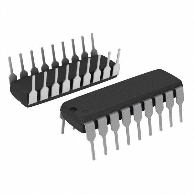
| 供应商器件封装 | 8-SOIC |
| 关闭 | Yes |
| 其它名称 | 296-26338-2 |
| 功能 | Transceiver |
| 包装 | 带卷 (TR) |
| 协议 | RS485 |
| 单位重量 | 72.600 mg |
| 双工 | 半 |
| 商标 | Texas Instruments |
| 安装类型 | 表面贴装 |
| 安装风格 | SMD/SMT |
| 封装 | Reel |
| 封装/外壳 | 8-SOIC(0.154",3.90mm 宽) |
| 封装/箱体 | SOIC-8 |
| 工作温度 | -40°C ~ 85°C |
| 工作温度范围 | - 40 C to + 85 C |
| 工作电源电压 | 3.3 V |
| 工厂包装数量 | 2500 |
| 接收器滞后 | 35mV |
| 接收机数量 | 1 Receiver |
| 数据速率 | 1Mbps |
| 最大工作温度 | + 85 C |
| 最小工作温度 | - 40 C |
| 标准包装 | 2,500 |
| 激励器数量 | 1 Driver |
| 电压-电源 | 3 V ~ 3.6 V |
| 电源电流 | 15.5 mA |
| 类型 | 收发器 |
| 系列 | SN65HVD12 |
| 驱动器/接收器数 | 1/1 |


- 商务部:美国ITC正式对集成电路等产品启动337调查
- 曝三星4nm工艺存在良率问题 高通将骁龙8 Gen1或转产台积电
- 太阳诱电将投资9.5亿元在常州建新厂生产MLCC 预计2023年完工
- 英特尔发布欧洲新工厂建设计划 深化IDM 2.0 战略
- 台积电先进制程称霸业界 有大客户加持明年业绩稳了
- 达到5530亿美元!SIA预计今年全球半导体销售额将创下新高
- 英特尔拟将自动驾驶子公司Mobileye上市 估值或超500亿美元
- 三星加码芯片和SET,合并消费电子和移动部门,撤换高东真等 CEO
- 三星电子宣布重大人事变动 还合并消费电子和移动部门
- 海关总署:前11个月进口集成电路产品价值2.52万亿元 增长14.8%


PDF Datasheet 数据手册内容提取
Product Order Technical Tools & Support & Folder Now Documents Software Community SN65HVD10,SN65HVD11,SN65HVD12 SN75HVD10,SN75HVD11,SN75HVD12 SLLS505O–FEBRUARY2002–REVISEDFEBRUARY2017 SNx5HVD1x 3.3-V RS-485 Transceivers 1 Features 3 Description • OperatesWitha3.3-VSupply The SN65HVD10, SN75HVD10, SN65HVD11, 1 SN75HVD11, SN65HVD12, and SN75HVD12 bus • Bus-PinESDProtectionExceeds16-kVHBM transceivers combine a 3-state differential line driver • 1/8Unit-LoadOptionAvailable(Upto256Nodes and differential input line receiver that operate with a ontheBus) single 3.3-V power supply. They are designed for • OptionalDriverOutputTransitionTimesfor balanced transmission lines and meet or exceed ANSI standard TIA/EIA-485-A and ISO 8482:1993. SignalingRates (1)of1Mbps,10Mbps,and These differential bus transceivers are monolithic 32Mbps integrated circuits designed for bidirectional data • MeetsorExceedstheRequirementsofANSI communication on multipoint bus-transmission lines. TIA/EIA-485-A The drivers and receivers have active-high and • Bus-PinShort-CircuitProtectionFrom –7Vto active-low enables, respectively, that can be 12V externally connected together to function as direction control. Very low device standby supply current can • Low-CurrentStandbyMode:1µA,Typical beachievedbydisablingthedriverandthereceiver. • Open-Circuit,Idle-Bus,andShorted-BusFailsafe The driver differential outputs and receiver differential Receiver inputs connect internally to form a differential input/ • ThermalShutdownProtection output (I/O) bus port that is designed to offer • Glitch-FreePower-UpandPower-DownProtection minimum loading to the bus whenever the driver is forHot-PluggingApplications disabledorV =0.Thesepartsfeaturewidepositive CC and negative common-mode voltage ranges making • SN75176Footprint themsuitableforparty-lineapplications. 2 Applications DeviceInformation(1) • DigitalMotorControl PARTNUMBER PACKAGE BODYSIZE(NOM) • UtilityMeters SN65HVD10 • Chassis-to-ChassisInterconnects SN65HVD11 SOIC(8) 4.90mm×3.91mm • ElectronicSecurityStations SN65HVD12 • IndustrialProcessControl SN75HVD10 • BuildingAutomation SN75HVD11 PDIP(8) 9.81mm×6.35mm • Point-of-Sale(POS)TerminalsandNetworks SN75HVD12 (1) Thesignalingrateofalineisthenumberofvoltage (1) For all available packages, see the orderable addendum at transitionsthataremadepersecondexpressedintheunits theendofthedatasheet. bps(bitspersecond). TypicalApplicationDiagram R R R R A A RE RE B RT RT B DE DE D D D D A B A B R R D D R RE DE D R RE DE D Copyright © 2016, Texas Instruments Incorporated 1 An IMPORTANT NOTICE at the end of this data sheet addresses availability, warranty, changes, use in safety-critical applications, intellectualpropertymattersandotherimportantdisclaimers.PRODUCTIONDATA.
SN65HVD10,SN65HVD11,SN65HVD12 SN75HVD10,SN75HVD11,SN75HVD12 SLLS505O–FEBRUARY2002–REVISEDFEBRUARY2017 www.ti.com Table of Contents 1 Features.................................................................. 1 9.2 FunctionalBlockDiagram.......................................17 2 Applications........................................................... 1 9.3 FeatureDescription.................................................17 3 Description............................................................. 1 9.4 DeviceFunctionalModes........................................17 4 RevisionHistory..................................................... 2 10 ApplicationandImplementation........................ 19 10.1 ApplicationInformation..........................................19 5 DeviceComparisonTable..................................... 3 10.2 TypicalApplication................................................20 6 PinConfigurationandFunctions......................... 3 11 PowerSupplyRecommendations..................... 23 7 Specifications......................................................... 4 12 Layout................................................................... 23 7.1 AbsoluteMaximumRatings......................................4 12.1 LayoutGuidelines.................................................23 7.2 ESDRatings..............................................................4 12.2 LayoutExample....................................................24 7.3 RecommendedOperatingConditions.......................4 12.3 ThermalConsiderations........................................24 7.4 ThermalInformation..................................................5 13 DeviceandDocumentationSupport................. 26 7.5 DriverElectricalCharacteristics................................5 7.6 ReceiverElectricalCharacteristics...........................6 13.1 DeviceSupport......................................................26 7.7 PowerDissipationCharacteristics............................6 13.2 RelatedLinks........................................................26 7.8 DriverSwitchingCharacteristics...............................7 13.3 ReceivingNotificationofDocumentationUpdates26 7.9 ReceiverSwitchingCharacteristics...........................8 13.4 CommunityResources..........................................26 7.10 DissipationRatings.................................................8 13.5 Trademarks...........................................................26 7.11 TypicalCharacteristics............................................9 13.6 ElectrostaticDischargeCaution............................26 13.7 Glossary................................................................26 8 ParameterMeasurementInformation................11 14 Mechanical,Packaging,andOrderable 9 DetailedDescription............................................ 17 Information........................................................... 27 9.1 Overview.................................................................17 4 Revision History ChangesfromRevisionN(July2015)toRevisionO Page • AddedMINvalueof–55°CtotheStoragetemperatureinAbsoluteMaximumRatings........................................................ 4 ChangesfromRevisionM(July2013)toRevisionN Page • AddedPinConfigurationandFunctionssection,ESDRatingstable,FeatureDescriptionsection,DeviceFunctional Modes,ApplicationandImplementationsection,PowerSupplyRecommendationssection,Layoutsection,Device andDocumentationSupportsection,andMechanical,Packaging,andOrderableInformationsection .............................. 1 ChangesfromRevisionL(July2013)toRevisionM Page • ChangedtheV TYPvalueFrom:–0.65VTo:–0.065V ................................................................................................... 6 IT+ ChangesfromRevisionK(September2011)toRevisionL Page • AddedTYP=–0.65VtoV ................................................................................................................................................ 6 IT+ • AddedTYP=–0.1VtoV ................................................................................................................................................... 6 IT– ChangesfromRevisionJ(February2009)toRevisionK Page • Addednewsection'LOW-POWERSTANDBYMODE',intheApplicationInformationsection........................................... 18 2 SubmitDocumentationFeedback Copyright©2002–2017,TexasInstrumentsIncorporated ProductFolderLinks:SN65HVD10 SN65HVD11 SN65HVD12SN75HVD10 SN75HVD11 SN75HVD12
SN65HVD10,SN65HVD11,SN65HVD12 SN75HVD10,SN75HVD11,SN75HVD12 www.ti.com SLLS505O–FEBRUARY2002–REVISEDFEBRUARY2017 5 Device Comparison Table PARTNUMBER SIGNALINGRATE UNITLOADS T SOICMARKING SOIC(1) PDIP A SN65HVD10D SN65HVD10P 32Mbps 1/2 VP10 SN65HVD11D SN65HVD11P 10Mbps 1/8 –40°Cto85°C VP11 SN65HVD12D SN65HVD12P 1Mbps 1/8 VP12 SN75HVD10D SN75HVD10P 32Mbps 1/2 VN10 SN75HVD11D SN75HVD11P 10Mbps 1/8 –0°Cto70°C VN11 SN75HVD12D SN75HVD12P 1Mbps 1/8 VN12 SN65HVD10QD SN65HVD10QP 32Mbps 1/2 VP10Q –40°Cto125°C SN65HVD11QD SN65HVD11QP 10Mbps 1/8 VP11Q (1) TheDpackageisavailableasatapeandreel.AddanRsuffixtothepartnumber(thatis,SN75HVD11DR)forthisoption. 6 Pin Configuration and Functions D,JD,orHKJPackage 8-PinSOICorPDIP TopView R 1 8 VCC RE 2 7 B DE 3 6 A D 4 5 GND PinFunctions PIN TYPE DESCRIPTION NAME NO. A 6 Businput/output Driveroutputorreceiverinput(complementarytoB) B 7 Businput/output Driveroutputorreceiverinput(complementarytoA) D 4 Digitalinput Driverdatainput DE 3 Digitalinput Active-highdriverenable GND 5 Referencepotential Localdeviceground R 1 Digitaloutput Receivedataoutput RE 2 Digitalinput Active-lowreceiverenable V 8 Supply 3-Vto3.6-Vsupply CC Copyright©2002–2017,TexasInstrumentsIncorporated SubmitDocumentationFeedback 3 ProductFolderLinks:SN65HVD10 SN65HVD11 SN65HVD12SN75HVD10 SN75HVD11 SN75HVD12
SN65HVD10,SN65HVD11,SN65HVD12 SN75HVD10,SN75HVD11,SN75HVD12 SLLS505O–FEBRUARY2002–REVISEDFEBRUARY2017 www.ti.com 7 Specifications 7.1 Absolute Maximum Ratings overoperatingfree-airtemperaturerangeunlessotherwisenoted (1) (2) MIN MAX UNIT V Supplyvoltage –0.3 6 V CC VoltageatAorB –9 14 V InputvoltageatD,DE,R,orRE –0.5 V +0.5 V CC Voltageinput,transientpulse,AandB,through100Ω,seeFigure22 –50 50 V I Receiveroutputcurrent –11 11 mA O Continuoustotalpowerdissipation SeeDissipationRatings T Junctiontemperature 170 °C J T Storagetemperature –55 145 °C stg (1) StressesbeyondthoselistedunderAbsoluteMaximumRatingsmaycausepermanentdamagetothedevice.Thesearestressratings only,andfunctionaloperationofthedeviceattheseoranyotherconditionsbeyondthoseindicatedunderRecommendedOperating Conditionsisnotimplied.Exposuretoabsolute-maximum-ratedconditionsforextendedperiodsmayaffectdevicereliability. (2) Allvoltagevalues,exceptdifferentialI/Obusvoltages,arewithrespecttonetworkgroundterminal. 7.2 ESD Ratings VALUE UNIT Pins5,6,and7 ±16000 Humanbodymodel(HBM),perANSI/ESDA/JEDECJS-001(1) Allpins ±4000 Electrostatic V(ESD) discharge CJEhSaDrg2e2d-Cde1v0i1ce(2)model(CDM),perJEDECspecification Allpins ±1000 V Electricalfasttransient/burst(3) Pins5,6,and7 ±4000 (1) JEDECdocumentJEP155statesthat500-VHBMallowssafemanufacturingwithastandardESDcontrolprocess. (2) JEDECdocumentJEP157statesthat250-VCDMallowssafemanufacturingwithastandardESDcontrolprocess. (3) TestedinaccordancewithIEC61000-4-4. 7.3 Recommended Operating Conditions overoperatingfree-airtemperaturerangeunlessotherwisenoted MIN NOM MAX UNIT V Supplyvoltage 3 3.6 CC V orV Voltageatanybusterminal(separatelyorcommonmode) –7(1) 12 I IC V High-levelinputvoltage D,DE,RE 2 V V IH CC V Low-levelinputvoltage D,DE,RE 0 0.8 IL V Differentialinputvoltage SeeFigure18 –12 12 ID Driver –60 I High-leveloutputcurrent mA OH Receiver –8 Driver 60 I Low-leveloutputcurrent mA OL Receiver 8 R Differentialloadresistance 54 60 Ω L C Differentialloadcapacitance 50 pF L HVD10 32 Signalingrate HVD11 10 Mbps HVD12 1 T (2) Junctiontemperature 145 °C J (1) Thealgebraicconvention,inwhichtheleastpositive(mostnegative)limitisdesignatedasminimumisusedinthisdatasheet. (2) Seethermalcharacteristicstableforinformationregardingthisspecification. 4 SubmitDocumentationFeedback Copyright©2002–2017,TexasInstrumentsIncorporated ProductFolderLinks:SN65HVD10 SN65HVD11 SN65HVD12SN75HVD10 SN75HVD11 SN75HVD12
SN65HVD10,SN65HVD11,SN65HVD12 SN75HVD10,SN75HVD11,SN75HVD12 www.ti.com SLLS505O–FEBRUARY2002–REVISEDFEBRUARY2017 7.4 Thermal Information SNx5HVD1xx THERMALMETRIC D(SOIC) P(PDIP) UNIT 8Pins 8Pins High−Kboard(2),Noairflow 121 R Junction-to-ambientthermalresistance(1) °C/W θJA Noairflow(3) 93 High−Kboard 67 R Junction-to-boardthermalresistance °C/W θJB See (3) 57 R Junction-to-casethermalresistance 41 55 °C/W θJC (1) TheintentofR specificationissolelyforathermalperformancecomparisonofonepackagetoanotherinastandardized θJA environment.Thismethodologyisnotmeanttoandwillnotpredicttheperformanceofapackageinanapplication-specificenvironment. (2) JSD51−7,HighEffectiveThermalConductivityTestBoardforLeadedSurfaceMountPackages. (3) JESD51−10,TestBoardsforThrough-HolePerimeterLeadedPackageThermalMeasurements. 7.5 Driver Electrical Characteristics overrecommendedoperatingconditionsunlessotherwisenoted PARAMETER TESTCONDITIONS MIN TYP(1) MAX UNIT V Inputclampvoltage I =–18mA –1.5 V IK I I =0 2 V O CC |V | Differentialoutputvoltage(2) R =54Ω,SeeFigure11 1.5 V OD L V =–7Vto12V,SeeFigure12 1.5 test Changeinmagnitudeofdifferentialoutput Δ|V | SeeFigure11andFigure12 –0.2 0.2 V OD voltage V Peak-to-peakcommon-modeoutputvoltage 400 mV OC(PP) V Steady-statecommon-modeoutputvoltage 1.4 2.5 V OC(SS) SeeFigure13 Changeinsteady-statecommon-mode ΔV –0.05 0.05 V OC(SS) outputvoltage I High-impedanceoutputcurrent Seereceiverinputcurrents OZ D –100 0 I Inputcurrent μA I DE 0 100 I Short-circuitoutputcurrent –7V≤V ≤12V –250 250 mA OS O C Differentialoutputcapacitance V =0.4sin(4E6πt)+0.5V,DEat0V 16 pF (OD) OD REatV , CC Receiverdisabledand DandDEatV 9 15.5 mA CC, driverenabled Noload REatV , CC Receiverdisabledand DatV , I Supplycurrent CC driverdisabled 1 5 μA CC DEat0V, (standby) Noload REat0V, Receiverenabledand DandDEatV , 9 15.5 mA CC driverenabled Noload (1) Alltypicalvaluesareat25°Candwitha3.3-Vsupply. (2) ForT >85°C,V is±5%. A CC Copyright©2002–2017,TexasInstrumentsIncorporated SubmitDocumentationFeedback 5 ProductFolderLinks:SN65HVD10 SN65HVD11 SN65HVD12SN75HVD10 SN75HVD11 SN75HVD12
SN65HVD10,SN65HVD11,SN65HVD12 SN75HVD10,SN75HVD11,SN75HVD12 SLLS505O–FEBRUARY2002–REVISEDFEBRUARY2017 www.ti.com 7.6 Receiver Electrical Characteristics overrecommendedoperatingconditionsunlessotherwisenoted PARAMETER TESTCONDITIONS MIN TYP(1) MAX UNIT V Positive-goinginputthresholdvoltage I =–8mA –0.065 –0.01 IT+ O Negative-goinginputthreshold V V I =8mA –0.2 –0.1 IT– voltage O V Hysteresisvoltage(V –V ) 35 mV hys IT+ IT– V Enable-inputclampvoltage I =–18mA –1.5 V IK I V High-leveloutputvoltage V =200mV,I =–8mA,seeFigure18 2.4 V OH ID OH V Low-leveloutputvoltage V =–200mV,I =8mA,seeFigure18 0.4 V OL ID OL I High-impedance-stateoutputcurrent V =0orV ,REatV –1 1 μA OZ O CC CC V orV =12V 0.05 0.11 A B VAorVB=12V,VCC=0V HVD11,HVD12, 0.06 0.13 mA V orV =–7V Otherinputsat0V –0.1 –0.05 A B V orV =–7V,V =0V –0.05 –0.04 A B CC I Businputcurrent I V orV =12V 0.2 0.5 A B VAorVB=12V,VCC=0V HVD10, 0.25 0.5 mA V orV =–7V Otherinputsat0V –0.4 –0.2 A B V orV =–7V,V =0V –0.4 –0.15 A B CC I High-levelinputcurrent,RE V =2V –30 0 μA IH IH I Low-levelinputcurrent,RE V =0.8V –30 0 μA IL IL C Differentialinputcapacitance V =0.4sin(4E6πt)+0.5V,DEat0V 15 pF ID ID REat0V Receiverenabledanddriver DandDEat0V 4 8 mA disabled Noload REatV CC DatV Receiverdisabledanddriver I Supplycurrent CC 1 5 μA CC DEat0V disabled(standby) Noload REat0V Receiverenabledanddriver DandDEatV 9 15.5 mA CC enabled Noload (1) Alltypicalvaluesareat25°Candwitha3.3-Vsupply. 7.7 Power Dissipation Characteristics PARAMETER TESTCONDITIONS MIN TYP MAX UNIT HVD10 198 250 RL=60Ω,CL=50pF, (32Mbps) DEatV ,REat0V, CC HVD11 P Devicepowerdissipation InputtoDisa50%duty-cycle 141 176 mW D (10Mbps) squarewaveatindicatedsignaling rate HVD12 133 161 (500kbps) High-Kboard,noairflow Dpkg –40 116 T Ambientairtemperature(1) °C A Noairflow(2) Ppkg –40 123 T Thermalshutdownjunctiontemperature(1) 165 °C JSD (1) SeeThermalCharacteristicsofICPackagessectionforanexplanationoftheseparameters. (2) JESD51−10,TestBoardsforThrough-HolePerimeterLeadedPackageThermalMeasurements. 6 SubmitDocumentationFeedback Copyright©2002–2017,TexasInstrumentsIncorporated ProductFolderLinks:SN65HVD10 SN65HVD11 SN65HVD12SN75HVD10 SN75HVD11 SN75HVD12
SN65HVD10,SN65HVD11,SN65HVD12 SN75HVD10,SN75HVD11,SN75HVD12 www.ti.com SLLS505O–FEBRUARY2002–REVISEDFEBRUARY2017 7.8 Driver Switching Characteristics overrecommendedoperatingconditionsunlessotherwisenoted PARAMETER TESTCONDITIONS MIN TYP(1) MAX UNIT HVD10 5 8.5 16 Propagationdelaytime, t HVD11 18 25 40 ns PLH low-to-high-leveloutput HVD12 135 200 300 HVD10 5 8.5 16 Propagationdelaytime, t HVD11 18 25 40 ns PHL high-to-low-leveloutput HVD12 135 200 300 HVD10 3 4.5 10 Differentialoutputsignal R =54Ω,C =50pF t HVD11 L L 10 20 30 ns r risetime SeeFigure14 HVD12 100 170 300 HVD10 3 4.5 10 Differentialoutputsignal t HVD11 10 20 30 ns f falltime HVD12 100 170 300 HVD10 1.5 t Pulseskew(|t –t |) HVD11 2.5 ns sk(p) PHL PLH HVD12 7 HVD10 6 t (2) Part-to-partskew HVD11 11 ns sk(pp) HVD12 100 HVD10 31 Propagationdelaytime, t high-impedance-to-high- HVD11 55 ns PZH leveloutput HVD12 R =110Ω,REat0V 300 L HVD10 SeeFigure15 25 Propagationdelaytime, t high-level-to-high- HVD11 55 ns PHZ impedanceoutput HVD12 300 HVD10 26 Propagationdelaytime, t high-impedance-to-low- HVD11 55 ns PZL leveloutput HVD12 R =110Ω,REat0V 300 L HVD10 SeeFigure16 26 Propagationdelaytime, t low-level-to-high- HVD11 75 ns PLZ impedanceoutput HVD12 400 Propagationdelaytime,standby-to-high- R =110Ω,REat3V t L 6 μs PZH leveloutput SeeFigure15 Propagationdelaytime,standby-to-low- R =110Ω,REat3V t L 6 μs PZL leveloutput SeeFigure16 (1) Alltypicalvaluesareat25°Candwitha3.3-Vsupply. (2) t isthemagnitudeofthedifferenceinpropagationdelaytimesbetweenanyspecifiedterminalsoftwodeviceswhenbothdevices sk(pp) operatewiththesamesupplyvoltages,atthesametemperature,andhaveidenticalpackagesandtestcircuits. Copyright©2002–2017,TexasInstrumentsIncorporated SubmitDocumentationFeedback 7 ProductFolderLinks:SN65HVD10 SN65HVD11 SN65HVD12SN75HVD10 SN75HVD11 SN75HVD12
SN65HVD10,SN65HVD11,SN65HVD12 SN75HVD10,SN75HVD11,SN75HVD12 SLLS505O–FEBRUARY2002–REVISEDFEBRUARY2017 www.ti.com 7.9 Receiver Switching Characteristics overrecommendedoperatingconditionsunlessotherwisenoted PARAMETER TESTCONDITIONS MIN TYP(1) MAX UNIT Propagationdelaytime, t HVD10 12.5 20 25 PLH low-to-high-leveloutput ns Propagationdelaytime, t HVD10 12.5 20 25 PHL high-to-low-leveloutput Propagationdelaytime, HVD11 tPLH low-to-high-leveloutput HVD12 VID=–1.5Vto1.5V 30 55 70 ns C =15pF L Propagationdelaytime, HVD11 SeeFigure19 t 30 55 70 ns PHL high-to-low-leveloutput HVD12 HVD10 1.5 t Pulseskew(|t –t |) HVD11 4 ns sk(p) PHL PLH HVD12 4 HVD10 8 t (2) Part-to-partskew HVD11 15 ns sk(pp) HVD12 15 tr Outputsignalrisetime CL=15pF 1 2 5 ns t Outputsignalfalltime SeeFigure19 1 2 5 f t (1) Outputenabletimetohighlevel 15 PZH tPZL (1) Outputenabletimetolowlevel CL=15pF,DEat3V 15 ns t Outputdisabletimefromhighlevel SeeFigure20 20 PHZ t Outputdisabletimefromlowlevel 15 PLZ t (2) Propagationdelaytime,standby-to-high- 6 PZH leveloutput C =15pF,DEat0 L μs t (2) Propagationdelaytime,standby-to-low- SeeFigure21 6 PZL leveloutput (1) Alltypicalvaluesareat25°Candwitha3.3-Vsupply (2) t isthemagnitudeofthedifferenceinpropagationdelaytimesbetweenanyspecifiedterminalsoftwodeviceswhenbothdevices sk(pp) operatewiththesamesupplyvoltages,atthesametemperature,andhaveidenticalpackagesandtestcircuits. 7.10 Dissipation Ratings T ≤25°C DERATINGFACTOR(1) T =70°C T =85°C T =125°C PACKAGE A A A A POWERRATING ABOVET =25°C POWERRATING POWERRATING POWERRATING A D(2) 597mW 4.97mW/°C 373mW 298mW 100mW D(3) 990mW 8.26mW/°C 620mW 496mW 165mW P 1290mW 10.75mW/°C 806mW 645mW 215mW (1) Thisistheinverseofthejunction-to-ambientthermalresistancewhenboard-mountedandwithnoairflow. (2) TestedinaccordancewiththeLow-KthermalmetricdefinitionsofEIA/JESD51-3. (3) TestedinaccordancewiththeHigh-KthermalmetricdefinitionsofEIA/JESD51-7. 8 SubmitDocumentationFeedback Copyright©2002–2017,TexasInstrumentsIncorporated ProductFolderLinks:SN65HVD10 SN65HVD11 SN65HVD12SN75HVD10 SN75HVD11 SN75HVD12
SN65HVD10,SN65HVD11,SN65HVD12 SN75HVD10,SN75HVD11,SN75HVD12 www.ti.com SLLS505O–FEBRUARY2002–REVISEDFEBRUARY2017 7.11 Typical Characteristics 70 70 TA= 25°C RL= 54W TA= 25°C RL= 54W REat VCC CL= 50 pF REat VCC CL= 50 pF VCC= 3.6 V A DE at VCC mA DE at VCC m nt− 60 VCC= 3.6 V ent− 60 urre Curr ply C 50 pply 50 p u MS Su VCC= 3 V RMS S VCC= 3 V R − −CC 40 VCC= 3.3 V ICC 40 VCC= 3.3 V I 30 30 0 5 10 15 20 25 30 35 40 0 2.5 5 7.5 10 Signaling Rate−Mbps Signaling Rate−Mbps Figure1.HVD10RMSSupplyCurrentvsSignalingRate Figure2.HVD11RMSSupplyCurrentvsSignalingRate 70 300 TA= 25°C RL= 54W TA= 25°C REat VCC CL= 50 pF 250 DE at 0 V DE at VCC −mA 60 VCC= 3.6 V mA 200 nt − 150 VCC= 0 V y Curre VCC= 3.3 V Current 100 S Suppl 50 VCC= 3 V s Input 500 VCC= 3.3 V M u R B − − −50 CC 40 II I −100 −150 30 −200 100 400 700 1000 −7−6−5−4−3−2−1 0 1 2 3 4 5 6 7 8 9101112 Signaling Rate−kbps VI−Bus Input Voltage−V Figure3.HVD12RMSSupplyCurrentvsSignalingRate Figure4.HVD10BusInputCurrentvsBusInputVoltage 90 150 80 TA= 25°C TA = 25°C 70 DE at 0 V mA 100 DE at VCC mAput Current− 123456000000 VCC= 0 V el Output Current − 500 DVC aCt =V C3C.3 V s In 0 VCC= 3.3 V Lev −50 Bu −10 gh- −II −20 − Hi −100 −30 H O −40 I −150 −50 −60 −200 −7−6−5−4−3−2−1 0 1 2 3 4 5 6 7 8 9101112 −4 −2 0 2 4 6 VI−Bus Input Voltage−V VOH − Driver High-Level Output Voltage − V Figure5.HVD11orHVD12BusInputCurrentvsBusInput Figure6.High-LevelOutputCurrentvsDriverHigh-Level Voltage OutputVoltage Copyright©2002–2017,TexasInstrumentsIncorporated SubmitDocumentationFeedback 9 ProductFolderLinks:SN65HVD10 SN65HVD11 SN65HVD12SN75HVD10 SN75HVD11 SN75HVD12
SN65HVD10,SN65HVD11,SN65HVD12 SN75HVD10,SN75HVD11,SN75HVD12 SLLS505O–FEBRUARY2002–REVISEDFEBRUARY2017 www.ti.com Typical Characteristics (continued) 200 2.5 A 180 TDAE =a t2 5V°CCC 2.4 VDCEC a =t V3C.3C V el Output Current − m 11118024600000 DVC aCt =0 3V.3 V Differential Output − V 2222....0123 D at VCC Low-Lev 4600 − Driver 11..89 − D OL 20 VO 1.7 I 0 1.6 −20 1.5 −4 −2 0 2 4 6 8 −40 −15 10 35 60 85 VOL − Driver Low-Level Output Voltage − V TA − Free-Air Temperature − °C Figure7.Low-LevelOutputCurrentvsDriverLow-Level Figure8.DriverDifferentialOutputvsFree-AirTemperature OutputVoltage −40 600 TA = 25°C −35 DE at VCC − mA −30 DR La =t V5C4C W 500 HVD12 nt Curre −25 −ns 400 HVD11 ut me Outp −20 e Ti 300 ver −15 nabl HVD10 Dri E 200 − O −10 I 100 −5 0 0 0 0.50 1 1.50 2 2.50 3 3.50 -7 -2 3 8 13 VCC − Supply Voltage − V V(TEST)−Common-Mode Voltage−V Figure9.DriverOutputCurrentvsSupplyVoltage Figure10.EnableTimevsCommon-ModeVoltage 10 SubmitDocumentationFeedback Copyright©2002–2017,TexasInstrumentsIncorporated ProductFolderLinks:SN65HVD10 SN65HVD11 SN65HVD12SN75HVD10 SN75HVD11 SN75HVD12
SN65HVD10,SN65HVD11,SN65HVD12 SN75HVD10,SN75HVD11,SN75HVD12 www.ti.com SLLS505O–FEBRUARY2002–REVISEDFEBRUARY2017 8 Parameter Measurement Information V CC DE I II A OA 0 or 3V VOD 54Ω±1% B I OB V I V V OB OA Copyright © 2017,Texas Instruments Incorporated Figure11. DriverV TestCircuitandVoltageandCurrentDefinitions OD 375Ω±1% VCC DE A D 0 or 3 V VOD 60Ω±1% + B _ −7 V < V(test)< 12 V 375Ω±1% Copyright © 2017,Texas Instruments Incorporated Figure12. DriverV WithCommon-ModeLoadingTestCircuit OD A VA VCC 27Ω±1% DE B VB A Input D VOC(PP) DVOC(SS) 27Ω±1% B VOC CL= 50 pF±20% VOC CLIncludes Fixture and Instrumentation Capacitance Copyright © 2017,Texas Instruments Incorporated Input:PRR=500kHz,50%DutyCycle,t <60ns,t <6nsZ =50Ω r f O Figure13. TestCircuitandDefinitionsfortheDriverCommon-ModeOutputVoltage Copyright©2002–2017,TexasInstrumentsIncorporated SubmitDocumentationFeedback 11 ProductFolderLinks:SN65HVD10 SN65HVD11 SN65HVD12SN75HVD10 SN75HVD11 SN75HVD12
SN65HVD10,SN65HVD11,SN65HVD12 SN75HVD10,SN75HVD11,SN75HVD12 SLLS505O–FEBRUARY2002–REVISEDFEBRUARY2017 www.ti.com Parameter Measurement Information (continued) 3 V VCC DE CL= 50 pF±20% VI 1.5 V 1.5 V A D VOD CLIncludes Fixture tPLH tPHL GeInnepruattor VI 50Ω B R±L1%= 54Ω aCnadp aIncsittarunmceentation 0 V 90% 90% 0 V ≈2 V VOD 10% 10% ≈–2 V tr tf Copyright © 2017,Texas Instruments Incorporated Generator:PRR=500kHz,50%DutyCycle,t <60ns,t <6nsZ =50Ω r f O Figure14. DriverSwitchingTestCircuitandVoltageWaveforms 3 V A S1 3 V D VO VI 1.5 V 1.5 V B 0 V DE 0.5 V CL= 50 pF±20% RL= 110Ω tPZH GeInnepruattor VI 50Ω ±1% VOH CaLnIdn cIlnusdterusm Feixnttuarteion VO 2.3 V Capacitance ≈0 V tPHZ Copyright © 2017,Texas Instruments Incorporated Generator:PRR=500kHz,50%DutyCycle,t <60ns,t <6nsZ =50Ω r f O Figure15. DriverHigh-LevelEnableandDisableTimeTestCircuitandVoltageWaveforms 3 V RL= 110Ω ≈3 V ±1% A S1 VI 1.5 V 1.5 V D 3 V VO 0 V B DE tPZL tPLZ Input CL= 50 pF±20% ≈3 V Generator VI 50Ω 0.5 V aCndL IInnsctlurudmese nFtiaxttiuorne VO 2.3 V Capacitance VOL Copyright © 2017,Texas Instruments Incorporated Generator:PRR=500kHz,50%DutyCycle,t <60ns,t <6nsZ =50Ω r f O Figure16. DriverLow-LevelOutputEnableandDisableTimeTestCircuitandVoltageWaveforms 12 SubmitDocumentationFeedback Copyright©2002–2017,TexasInstrumentsIncorporated ProductFolderLinks:SN65HVD10 SN65HVD11 SN65HVD12SN75HVD10 SN75HVD11 SN75HVD12
SN65HVD10,SN65HVD11,SN65HVD12 SN75HVD10,SN75HVD11,SN75HVD12 www.ti.com SLLS505O–FEBRUARY2002–REVISEDFEBRUARY2017 Parameter Measurement Information (continued) 375Ω±1% Y -7 V < V < 12 V (TEST) D 60 W V 0 or 3 V OD ±1% Z DE 375Ω±1% Input V 50Ω Generator 50% t (diff) pZH V (high) OD 1.5 V 0 V t (diff) pZL -1.5 V V (low) OD Copyright © 2017,Texas Instruments Incorporated Thetimet isthemeasurefromDEtoV (x).V isvalidwhenitisgreaterthan1.5V. PZL(x) OD OD Figure17. DriverEnableTimefromDEtoV OD IA A VA R IO VID B VA+ VB VIC VB IB VO 2 Copyright © 2017,Texas Instruments Incorporated Figure18. ReceiverVoltageandCurrentDefinitions Copyright©2002–2017,TexasInstrumentsIncorporated SubmitDocumentationFeedback 13 ProductFolderLinks:SN65HVD10 SN65HVD11 SN65HVD12SN75HVD10 SN75HVD11 SN75HVD12
SN65HVD10,SN65HVD11,SN65HVD12 SN75HVD10,SN75HVD11,SN75HVD12 SLLS505O–FEBRUARY2002–REVISEDFEBRUARY2017 www.ti.com Parameter Measurement Information (continued) A Input R VO Generator VI 50Ω B 1.5 V CL= 15 pF±20% RE 0 V CLIncludes Fixture and Instrumentation Capacitance Generator: PRR = 500 kHz, 50% Duty Cycle, tr<6 ns, tf<6 ns, Zo= 50Ω 3 V VI 1.5 V 1.5 V 0 V tPLH tPHL VOH 90% 90% VO 1.5 V 1.5 V 10% 10% VOL tr tf Copyright © 2017,Texas Instruments Incorporated Figure19. ReceiverSwitchingTestCircuitandVoltageWaveforms 3 V 3 V DE A A 0 V or 3 V D R VO 1 kΩ ±1% S1 B CL= 15 pF±20% RE B CLIncludes Fixture and Instrumentation Input Capacitance Generator VI 50Ω Generator: PRR = 500 kHz, 50% Duty Cycle, tr<6 ns, tf<6 ns, Zo= 50Ω 3 V VI 1.5 V 1.5 V 0 V tPZH(1) tPHZ VOH D at 3 V VOH–0.5 V S1 to B VO 1.5 V ≈0 V tPZL(1) tPLZ ≈3 V D at 0 V VO 1.5 V S1 toA VOL+0.5 V VOL Copyright © 2017,Texas Instruments Incorporated Figure20. ReceiverEnableandDisableTimeTestCircuitandVoltageWaveformsWithDriversEnabled 14 SubmitDocumentationFeedback Copyright©2002–2017,TexasInstrumentsIncorporated ProductFolderLinks:SN65HVD10 SN65HVD11 SN65HVD12SN75HVD10 SN75HVD11 SN75HVD12
SN65HVD10,SN65HVD11,SN65HVD12 SN75HVD10,SN75HVD11,SN75HVD12 www.ti.com SLLS505O–FEBRUARY2002–REVISEDFEBRUARY2017 Parameter Measurement Information (continued) 3 V A A 0 V or 1.5 V R VO 1 kΩ ±1% S1 B 1.5 V or 0 V RE CL= 15 pF±20% B CLIncludes Fixture and Instrumentation Input Capacitance Generator VI 50Ω Generator: PRR = 100 kHz, 50% Duty Cycle, tr<6 ns, tf<6 ns, Zo= 50Ω 3 V VI 1.5 V 0 V tPZH(2) VOH Aat 1.5 V B at 0 V VO 1.5 V S1 to B GND tPZL(2) 3 V Aat 0 V B at 1.5 V VO 1.5 V S1 toA VOL Copyright © 2017,Texas Instruments Incorporated Figure21. ReceiverEnableTimeFromStandby(DriverDisabled) 0 V or 3 V RE A R B 100W ±1% Pulse Generator, 15ms Duration, + D 1% Duty Cycle _ tr, tf≤100 ns DE 3 V or 0 V Copyright © 2017,Texas Instruments Incorporated NOTE:Thistestisconductedtotestsurvivabilityonly.DatastabilityattheRoutputisnotspecified. Figure22. TestCircuit,TransientOverVoltageTest Copyright©2002–2017,TexasInstrumentsIncorporated SubmitDocumentationFeedback 15 ProductFolderLinks:SN65HVD10 SN65HVD11 SN65HVD12SN75HVD10 SN75HVD11 SN75HVD12
SN65HVD10,SN65HVD11,SN65HVD12 SN75HVD10,SN75HVD11,SN75HVD12 SLLS505O–FEBRUARY2002–REVISEDFEBRUARY2017 www.ti.com Parameter Measurement Information (continued) D and REInputs DE Input VCC VCC 100 kΩ 1 kΩ 1 kΩ Input Input 9 V 100 kΩ 9 V AInput B Input VCC VCC 16 V 16 V R1 R1 R3 R3 Input Input R2 R2 16 V 16 V Aand B Outputs R Output VCC VCC 16 V 5Ω Output Output 9 V 16 V R1/R2 R3 SN65HVD10 9 kW 45 kW SN65HVD11 36 kW 180 kW SN65HVD12 36 kW 180 kW Copyright © 2017,Texas Instruments Incorporated Figure23. EquivalentInputandOutputSchematicDiagrams 16 SubmitDocumentationFeedback Copyright©2002–2017,TexasInstrumentsIncorporated ProductFolderLinks:SN65HVD10 SN65HVD11 SN65HVD12SN75HVD10 SN75HVD11 SN75HVD12
SN65HVD10,SN65HVD11,SN65HVD12 SN75HVD10,SN75HVD11,SN75HVD12 www.ti.com SLLS505O–FEBRUARY2002–REVISEDFEBRUARY2017 9 Detailed Description 9.1 Overview The SN65HVD10, SN65HVD11, and SN65HVD12 are 3.3 V, half-duplex, RS-485 transceivers available in 3 speedgradessuitablefordatatransmissionupto32Mbps,10Mbps,and1Mbps,respectively. These devices have active-high driver enables and active-low receiver enables. A standby current of less than 5µAcanbeachievedbydisablingbothdriverandreceiver. 9.2 Functional Block Diagram 9.3 Feature Description Internal ESD protection circuits protect the transceiver bus terminals against ±16-kV Human Body Model (HBM) electrostaticdischargesand±4-kVelectricalfasttransients(EFT)accordingtoIEC61000-4-4. The SN65HVD1x half-duplex family provides internal biasing of the receiver input thresholds for open-circuit, bus-idle,orshort-circuitfailsafeconditions,andatypicalreceiverhysteresisof35mV. 9.4 Device Functional Modes When the driver enable pin, DE, is logic high, the differential outputs A and B follow the logic states at data input D.AlogichighatDcausesAtoturnhighandBtoturnlow.Inthiscasethedifferentialoutputvoltagedefinedas V = V – V is positive. When D is low, the output states reverse, B turns high, A becomes low, and V is OD A B OD negative. When DE is low, both outputs turn high-impedance. In this condition the logic state at D is irrelevant. The DE pin has an internal pulldown resistor to ground; thus, when left open, the driver is disabled (high-impedance) by default.TheDpinhasaninternalpullupresistortoV ;thus,whenleftopenwhilethedriverisenabled,outputA CC turnshighandBturnslow. Table1.DriverFunctions(1) INPUT ENABLE OUTPUTS FUNCTION D DE A B H H H L ActivelydrivebusHigh L H L H ActivelydrivebusLow X L Z Z Driverdisabled X OPEN Z Z Driverdisabledbydefault OPEN H H L ActivelydrivebusHighbydefault (1) H=highlevel;L=lowlevel;Z=highimpedance;X=irrelevant;?=indeterminate Copyright©2002–2017,TexasInstrumentsIncorporated SubmitDocumentationFeedback 17 ProductFolderLinks:SN65HVD10 SN65HVD11 SN65HVD12SN75HVD10 SN75HVD11 SN75HVD12
SN65HVD10,SN65HVD11,SN65HVD12 SN75HVD10,SN75HVD11,SN75HVD12 SLLS505O–FEBRUARY2002–REVISEDFEBRUARY2017 www.ti.com When the receiver enable pin, RE, is logic low, the receiver is enabled. When the differential input voltage defined as V = V – V is positive and higher than the positive input threshold, V , the receiver output, R, ID A B IT+ turns high. When V is negative and lower than the negative input threshold, V , the receiver output, R, turns ID IT– low.IfV isbetweenV andV ,theoutputisindeterminate. ID IT+ IT– When RE is logic high or left open, the receiver output is high-impedance and the magnitude and polarity of V ID are irrelevant. Internal biasing of the receiver inputs causes the output to go failsafe-high when the transceiver is disconnected from the bus (open-circuit), the bus lines are shorted (short-circuit), or the bus is not actively driven (idlebus). Table2.ReceiverFunctions(1) DIFFERENTIALINPUT ENABLE OUTPUT FUNCTION V =V –V RE R ID A B V >V L H ReceivevalidbusHigh ID IT+ V <V <V L ? Indeterminatebusstate IT– ID IT+ V <V L L ReceivevalidbusLow ID IT– X H Z Receiverdisabled X OPEN Z Receiverdisabledbydefault Open-circuitbus L H Fail-safehighoutput Short-circuitbus L H Fail-safehighoutput (1) H=highlevel;L=lowlevel;Z=highimpedance;X=irrelevant;?=indeterminate 9.4.1 Low-PowerStandbyMode When both the driver and receiver are disabled (DE low and RE high) the device is in standby mode. If the enable inputs are in this state for less than 60 ns, the device does not enter standby mode. This guards against inadvertently entering standby mode during driver or receiver enabling. Only when the enable inputs are held in thisstatefor300nsormore,thedeviceisassuredtobeinstandbymode.Inthislow-powerstandbymode,most internalcircuitryispowereddown,andthesupplycurrentistypicallylessthan1 µA.Wheneitherthedriverorthe receiverisre-enabled,theinternalcircuitrybecomesactive. 18 SubmitDocumentationFeedback Copyright©2002–2017,TexasInstrumentsIncorporated ProductFolderLinks:SN65HVD10 SN65HVD11 SN65HVD12SN75HVD10 SN75HVD11 SN75HVD12
SN65HVD10,SN65HVD11,SN65HVD12 SN75HVD10,SN75HVD11,SN75HVD12 www.ti.com SLLS505O–FEBRUARY2002–REVISEDFEBRUARY2017 10 Application and Implementation NOTE Information in the following applications sections is not part of the TI component specification, and TI does not warrant its accuracy or completeness. TI’s customers are responsible for determining suitability of components for their purposes. Customers should validateandtesttheirdesignimplementationtoconfirmsystemfunctionality. 10.1 Application Information The SN65HVD10, 'HVD11, and 'HVD12 are half-duplex RS-485 transceivers commonly used for asynchronous datatransmissions.Thedriverandreceiverenablepinsallowfortheconfigurationofdifferentoperatingmodes. R R R R R R RE A RE A RE A DE B DE B DE B D D D D D D a) Independent driver and b) Combined enable signals for c) Receiver always on receiver enable signals use as directional control pin Copyright © 2016, Texas Instruments Incorporated Figure24. Half-DuplexTransceiverConfigurations a. Using independent enable lines provides the most flexible control as it allows for the driver and the receiver to be turned on and off individually. While this configuration requires two control lines, it allows for selective listeningintothebustraffic,whetherthedriveristransmittingdataornot. b. Combining the enable signals simplifies the interface to the controller by forming a single direction-control signal. In this configuration, the transceiver operates as a driver when the direction-control line is high, and asareceiverwhenthedirection-controllineislow. c. Only one line is required when connecting the receiver-enable input to ground and controlling only the driver- enable input. In this configuration, a node not only receives the data from the bus, but also the data it sends andcanverifythatthecorrectdatahavebeentransmitted. Copyright©2002–2017,TexasInstrumentsIncorporated SubmitDocumentationFeedback 19 ProductFolderLinks:SN65HVD10 SN65HVD11 SN65HVD12SN75HVD10 SN75HVD11 SN75HVD12
SN65HVD10,SN65HVD11,SN65HVD12 SN75HVD10,SN75HVD11,SN75HVD12 SLLS505O–FEBRUARY2002–REVISEDFEBRUARY2017 www.ti.com 10.2 Typical Application An RS-485 bus consists of multiple transceivers connected in parallel to a bus cable. To eliminate line reflections, each cable end is terminated with a termination resistor, R , whose value matches the characteristic T impedance, Z , of the cable. This method, known as parallel termination, allows for higher data rates over a 0 longercablelength. R R R R A A RE RE B RT RT B DE DE D D D D A B A B R R D D R RE DE D R RE DE D Copyright © 2016, Texas Instruments Incorporated Figure25. TypicalRS-485NetworkWithHalf-DuplexTransceivers 10.2.1 DesignRequirements RS-485 is a robust electrical standard suitable for long-distance networking that may be used in a wide range of applicationswithvaryingrequirements,suchasdistance,datarate,andnumberofnodes. 10.2.1.1 DataRateandBusLength There is an inverse relationship between data rate and bus length, meaning the higher the data rate, the shorter the cable length; and conversely, the lower the data rate, the longer the cable may be without introducing data errors. While most RS-485 systems use data rates between 10 kbps and 100 kbps, some applications require data rates up to 250 kbps at distances of 4000 feet and longer. Longer distances are possible by allowing for smallsignaljitterofupto5or10%. 10000 5%, 10%, and 20% Jitter h (ft) 1000 gt Conservative n e Characteristics L e bl 100 a C 10 100 1k 10k 100k 1M 10M 100M Data Rate(bps) Figure26. CableLengthvsDataRateCharacteristic 20 SubmitDocumentationFeedback Copyright©2002–2017,TexasInstrumentsIncorporated ProductFolderLinks:SN65HVD10 SN65HVD11 SN65HVD12SN75HVD10 SN75HVD11 SN75HVD12
SN65HVD10,SN65HVD11,SN65HVD12 SN75HVD10,SN75HVD11,SN75HVD12 www.ti.com SLLS505O–FEBRUARY2002–REVISEDFEBRUARY2017 Typical Application (continued) 10.2.1.2 StubLength When connecting a node to the bus, the distance between the transceiver inputs and the cable trunk, known as the stub, should be as short as possible. Stubs present a nonterminated piece of bus line which can introduce reflections as the length of the stub increases. As a general guideline, the electrical length, or round-trip delay, of a stub should be less than one-tenth of the rise time of the driver, thus giving a maximum physical stub length as showninEquation1. L ≤0.1×t ×v×c (STUB) r where • t isthe10/90risetimeofthedriver r • visthesignalvelocityofthecableortraceasafactorofc • cisthespeedoflight(3×10⁸m/s) (1) Per Equation 1, Table 3 lists the maximum cable-stub lengths for the minimum-driver output rise-times of the SN65HVD1xfull-duplexfamilyoftransceiversforasignalvelocityof78%. Table3.MaximumStubLength MINIMUMDRIVEROUTPUT MAXIMUMSTUBLENGTH DEVICE RISETIME(ns) (m) (ft) SN65HVD10 3 0.07 0.23 SN65HVD11 10 0.23 0.75 SN65HVD12 100 2.34 7.67 10.2.1.3 BusLoading The RS-485 standard specifies that a compliant driver must be able to driver 32 unit loads (UL), where 1 unit load represents a load impedance of approximately 12 kΩ. Because the SN65HVD11 and HVD12 are each 1/8 UL transceivers, it is possible to connect up to 256 receivers to the bus. The SN65HVD10 is a 1/4 UL transceiver,andupto64receiversmaybeconnectedtothebus. 10.2.1.4 ReceiverFailsafe ThedifferentialreceiversoftheSN65HVD1xfamilyarefailsafetoinvalidbusstatescausedby: • Openbusconditions,suchasadisconnectedconnector • Shortedbusconditions,suchascabledamageshortingthetwisted-pairtogether • Idlebusconditionsthatoccurwhennodriveronthebusisactivelydriving. In any of these cases, the differential receiver will output a failsafe logic High state so that the output of the receiverisnotindeterminate. Receiver failsafe is accomplished by offsetting the receiver thresholds such that the input indeterminate range does not include zero volts differential. To comply with the RS-422 and RS-485 standards, the receiver output must output a High when the differential input V is more positive than +200 mV, and must output a Low when ID V is more negative than –200 mV. The receiver parameters which determine the failsafe performance are V ID IT(+) and V . As shown in Receiver Electrical Characteristics, differential signals more negative than –200 mV will IT(–) always cause a Low receiver output, and differential signals more positive than +200 mV will always cause a Highreceiveroutput. When the differential input signal is close to zero, it is still above the maximum V threshold of –10 mV, and IT(+) thereceiveroutputwillbeHigh. Copyright©2002–2017,TexasInstrumentsIncorporated SubmitDocumentationFeedback 21 ProductFolderLinks:SN65HVD10 SN65HVD11 SN65HVD12SN75HVD10 SN75HVD11 SN75HVD12
SN65HVD10,SN65HVD11,SN65HVD12 SN75HVD10,SN75HVD11,SN75HVD12 SLLS505O–FEBRUARY2002–REVISEDFEBRUARY2017 www.ti.com 10.2.2 DetailedDesignProcedure To protect bus nodes against high-energy transients, the implementation of external transient protection devices is therefore necessary. Figure 27 shows a protection circuit against 10-kV ESD (IEC 61000-4-2), 4-kV EFT (IEC 61000-4-4),and1-kVsurge(IEC61000-4-5)transients. Vcc Vcc 10k 0.1μF R1 RxD 1 R Vcc 8 TVS MCU 2 RE A 7 XCVR DIR 3 DE B 6 TxD 4 D GND 5 R2 10k Copyright © 2017,Texas Instruments Incorporated Figure27. TransientProtectionAgainstESD,EFT,andSurgeTransients Table4.BillofMaterials DEVICE FUNCTION ORDERNUMBER MANUFACTURER XCVR 3.3-V,full-duplexRS-485 SN65HVD1xD TI transceiver R1,R2 10-Ω,pulse-proof,thick-film CRCW0603010RJNEAHP Vishay resistor TVS Bidirectional400-W CDSOT23-SM712 Bourns transientsuppressor 10.2.3 ApplicationCurve Figure 28 demonstrates operation of the SN65HVD12 at a signaling rate of 250 kbps. Two SN65HVD12 transceivers are used to transmit data through a 2,000 foot (600 m) segment of Commscope 5524 category 5e+ twisted pair cable. The bus is terminated at each end by a 100-Ω resistor, matching the cable characteristic impedance. Driver Input Driver Output Receiver Input Receiver Output Figure28. SN65HVD12InputandOutputThrough2000FeetofCable 22 SubmitDocumentationFeedback Copyright©2002–2017,TexasInstrumentsIncorporated ProductFolderLinks:SN65HVD10 SN65HVD11 SN65HVD12SN75HVD10 SN75HVD11 SN75HVD12
SN65HVD10,SN65HVD11,SN65HVD12 SN75HVD10,SN75HVD11,SN75HVD12 www.ti.com SLLS505O–FEBRUARY2002–REVISEDFEBRUARY2017 11 Power Supply Recommendations To assure reliable operation at all data rates and supply voltages, each supply must be buffered with a 100-nF ceramic capacitor located as close to the supply pins as possible. The TPS76333 linear voltage regulator is suitableforthe3.3-Vsupply. 12 Layout 12.1 Layout Guidelines On-chip IEC-ESD protection is sufficient for laboratory and portable equipment but never sufficient for EFT and surgetransientsoccurringinindustrialenvironments.Therefore,robustandreliablebusnodedesignrequiresthe useofexternaltransientprotectiondevices. Because ESD and EFT transients have a wide frequency bandwidth from approximately 3 MHz to 3 GHz, high- frequencylayouttechniquesmustbeappliedduringPCBdesign. 1. Placetheprotectioncircuitryclosetothebusconnectortopreventnoisetransientsfromenteringtheboard. 2. Use V and ground planes to provide low-inductance. Note that high-frequency currents follow the path of CC leastinductanceandnotthepathofleastimpedance. 3. Design the protection components into the direction of the signal path. Do not force the transient currents to divertfromthesignalpathtoreachtheprotectiondevice. 4. Apply 100-nF to 220-nF bypass capacitors as close as possible to the V pins of transceiver, UART, and CC controllerICsontheboard. 5. Use at least two vias for V and ground connections of bypass capacitors and protection devices to CC minimizeeffectivevia-inductance. 6. Use 1-kΩ to 10-kΩ pull-up or pull-down resistors for enable lines to limit noise currents in these lines during transientevents. 7. Insert pulse-proof series resistors into the A and B bus lines if the TVS clamping voltage is higher than the specified maximum voltage of the transceiver bus terminals. These resistors limit the residual clamping currentintothetransceiverandpreventitfromlatchingup. 8. While pure TVS protection is sufficient for surge transients up to 1 kV, higher transients require metal-oxide varistors (MOVs) which reduce the transients to a few hundred volts of clamping voltage, and transient blockingunits(TBUs)thatlimittransientcurrenttolessthan1mA. Copyright©2002–2017,TexasInstrumentsIncorporated SubmitDocumentationFeedback 23 ProductFolderLinks:SN65HVD10 SN65HVD11 SN65HVD12SN75HVD10 SN75HVD11 SN75HVD12
SN65HVD10,SN65HVD11,SN65HVD12 SN75HVD10,SN75HVD11,SN75HVD12 SLLS505O–FEBRUARY2002–REVISEDFEBRUARY2017 www.ti.com 12.2 Layout Example 5 Via to ground R C 4 Via to VCC 6 R 1 R MCU 7 R MP 5 J R TVS 6 R XCVR 5 Figure29. SN65HVD1xLayoutExample 12.3 Thermal Considerations 12.3.1 ThermalCharacteristicsofICPackages R (Junction-to-AmbientThermalResistance) isdefinedasthedifferenceinjunctiontemperaturetoambient θJA temperaturedividedbytheoperatingpower. R isnotaconstantandisastrongfunctionof: θJA • thePCBdesign(50%variation) • altitude(20%variation) • devicepower(5%variation) R can be used to compare the thermal performance of packages if the specific test conditions are defined and θJA used. Standardized testing includes specification of PCB construction, test chamber volume, sensor locations, and the thermal characteristics of holding fixtures. R is often misused when it is used to calculate junction θJA temperaturesforotherinstallations. TI uses two test PCBs as defined by JEDEC specifications. The low-k board gives average in-use condition thermal performance, and it consists of a single copper trace layer 25 mm long and 2-oz thick. The high-k board gives best case in-use condition, and it consists of two 1-oz buried power planes with a single copper trace layer 25mmlongand2-ozthick.A4%to50%differenceinR canbemeasuredbetweenthesetwotestcards. θJA R (Junction-to-Case Thermal Resistance) is defined as difference in junction temperature to case divided θJC by the operating power. It is measured by putting the mounted package up against a copper block cold plate to forceheattoflowfromdie,throughthemoldcompoundintothecopperblock. R is a useful thermal characteristic when a heatsink is applied to package. It is not a useful characteristic to θJC predict junction temperature because it provides pessimistic numbers if the case temperature is measured in a nonstandardsystemandjunctiontemperaturesarebackedout.ItcanbeusedwithR in1-dimensionalthermal θJB simulationofapackagesystem. R (Junction-to-Board Thermal Resistance) is defined as the difference in the junction temperature and the θJB PCB temperature at the center of the package (closest to the die) when the PCB is clamped in a cold-plate structure.R isonlydefinedforthehigh-ktestcard. θJB R provides an overall thermal resistance between the die and the PCB. It includes a bit of the PCB thermal θJB resistance (especially for BGAs with thermal balls) and can be used for simple 1-dimensional network analysis of packagesystem,seeFigure30. 24 SubmitDocumentationFeedback Copyright©2002–2017,TexasInstrumentsIncorporated ProductFolderLinks:SN65HVD10 SN65HVD11 SN65HVD12SN75HVD10 SN75HVD11 SN75HVD12
SN65HVD10,SN65HVD11,SN65HVD12 SN75HVD10,SN75HVD11,SN75HVD12 www.ti.com SLLS505O–FEBRUARY2002–REVISEDFEBRUARY2017 Thermal Considerations (continued) Figure30. PCBThermalResistances Copyright©2002–2017,TexasInstrumentsIncorporated SubmitDocumentationFeedback 25 ProductFolderLinks:SN65HVD10 SN65HVD11 SN65HVD12SN75HVD10 SN75HVD11 SN75HVD12
SN65HVD10,SN65HVD11,SN65HVD12 SN75HVD10,SN75HVD11,SN75HVD12 SLLS505O–FEBRUARY2002–REVISEDFEBRUARY2017 www.ti.com 13 Device and Documentation Support 13.1 Device Support 13.1.1 Third-PartyProductsDisclaimer TI'S PUBLICATION OF INFORMATION REGARDING THIRD-PARTY PRODUCTS OR SERVICES DOES NOT CONSTITUTE AN ENDORSEMENT REGARDING THE SUITABILITY OF SUCH PRODUCTS OR SERVICES OR A WARRANTY, REPRESENTATION OR ENDORSEMENT OF SUCH PRODUCTS OR SERVICES, EITHER ALONEORINCOMBINATIONWITHANYTIPRODUCTORSERVICE. 13.2 Related Links The table below lists quick access links. Categories include technical documents, support and community resources,toolsandsoftware,andquickaccesstoordernow. Table5.RelatedLinks TECHNICAL TOOLS& SUPPORT& PARTS PRODUCTFOLDER ORDERNOW DOCUMENTS SOFTWARE COMMUNITY SN65HVD10 Clickhere Clickhere Clickhere Clickhere Clickhere SN65HVD11 Clickhere Clickhere Clickhere Clickhere Clickhere SN65HVD12 Clickhere Clickhere Clickhere Clickhere Clickhere SN75HVD10 Clickhere Clickhere Clickhere Clickhere Clickhere SN75HVD11 Clickhere Clickhere Clickhere Clickhere Clickhere SN75HVD12 Clickhere Clickhere Clickhere Clickhere Clickhere 13.3 Receiving Notification of Documentation Updates To receive notification of documentation updates, navigate to the device product folder on ti.com. In the upper right corner, click on Alert me to register and receive a weekly digest of any product information that has changed.Forchangedetails,reviewtherevisionhistoryincludedinanyreviseddocument. 13.4 Community Resources The following links connect to TI community resources. Linked contents are provided "AS IS" by the respective contributors. They do not constitute TI specifications and do not necessarily reflect TI's views; see TI's Terms of Use. TIE2E™OnlineCommunity TI'sEngineer-to-Engineer(E2E)Community.Createdtofostercollaboration amongengineers.Ate2e.ti.com,youcanaskquestions,shareknowledge,exploreideasandhelp solveproblemswithfellowengineers. DesignSupport TI'sDesignSupport QuicklyfindhelpfulE2Eforumsalongwithdesignsupporttoolsand contactinformationfortechnicalsupport. 13.5 Trademarks E2EisatrademarkofTexasInstruments. Allothertrademarksarethepropertyoftheirrespectiveowners. 13.6 Electrostatic Discharge Caution Thesedeviceshavelimitedbuilt-inESDprotection.Theleadsshouldbeshortedtogetherorthedeviceplacedinconductivefoam duringstorageorhandlingtopreventelectrostaticdamagetotheMOSgates. 13.7 Glossary SLYZ022—TIGlossary. Thisglossarylistsandexplainsterms,acronyms,anddefinitions. 26 SubmitDocumentationFeedback Copyright©2002–2017,TexasInstrumentsIncorporated ProductFolderLinks:SN65HVD10 SN65HVD11 SN65HVD12SN75HVD10 SN75HVD11 SN75HVD12
SN65HVD10,SN65HVD11,SN65HVD12 SN75HVD10,SN75HVD11,SN75HVD12 www.ti.com SLLS505O–FEBRUARY2002–REVISEDFEBRUARY2017 14 Mechanical, Packaging, and Orderable Information The following pages include mechanical, packaging, and orderable information. This information is the most current data available for the designated devices. This data is subject to change without notice and revision of thisdocument.Forbrowser-basedversionsofthisdatasheet,refertotheleft-handnavigation. Copyright©2002–2017,TexasInstrumentsIncorporated SubmitDocumentationFeedback 27 ProductFolderLinks:SN65HVD10 SN65HVD11 SN65HVD12SN75HVD10 SN75HVD11 SN75HVD12
PACKAGE OPTION ADDENDUM www.ti.com 24-Aug-2018 PACKAGING INFORMATION Orderable Device Status Package Type Package Pins Package Eco Plan Lead/Ball Finish MSL Peak Temp Op Temp (°C) Device Marking Samples (1) Drawing Qty (2) (6) (3) (4/5) SN65HVD10D ACTIVE SOIC D 8 75 Green (RoHS CU NIPDAU Level-1-260C-UNLIM -40 to 85 VP10 & no Sb/Br) SN65HVD10DG4 ACTIVE SOIC D 8 75 Green (RoHS CU NIPDAU Level-1-260C-UNLIM -40 to 85 VP10 & no Sb/Br) SN65HVD10DR ACTIVE SOIC D 8 2500 Green (RoHS CU NIPDAU Level-1-260C-UNLIM -40 to 85 VP10 & no Sb/Br) SN65HVD10DRG4 ACTIVE SOIC D 8 2500 Green (RoHS CU NIPDAU Level-1-260C-UNLIM -40 to 85 VP10 & no Sb/Br) SN65HVD10P ACTIVE PDIP P 8 50 Green (RoHS CU NIPDAU N / A for Pkg Type -40 to 85 65HVD10 & no Sb/Br) SN65HVD10QD ACTIVE SOIC D 8 75 Green (RoHS CU NIPDAU Level-1-260C-UNLIM -40 to 125 VP10Q & no Sb/Br) SN65HVD10QDG4 ACTIVE SOIC D 8 75 Green (RoHS CU NIPDAU Level-1-260C-UNLIM -40 to 125 VP10Q & no Sb/Br) SN65HVD10QDR ACTIVE SOIC D 8 2500 Green (RoHS CU NIPDAU Level-1-260C-UNLIM -40 to 125 VP10Q & no Sb/Br) SN65HVD11D ACTIVE SOIC D 8 75 Green (RoHS CU NIPDAU Level-1-260C-UNLIM -40 to 85 VP11 & no Sb/Br) SN65HVD11DG4 ACTIVE SOIC D 8 75 Green (RoHS CU NIPDAU Level-1-260C-UNLIM -40 to 85 VP11 & no Sb/Br) SN65HVD11DR ACTIVE SOIC D 8 2500 Green (RoHS CU NIPDAU Level-1-260C-UNLIM -40 to 85 VP11 & no Sb/Br) SN65HVD11DRG4 ACTIVE SOIC D 8 2500 Green (RoHS CU NIPDAU Level-1-260C-UNLIM -40 to 85 VP11 & no Sb/Br) SN65HVD11P ACTIVE PDIP P 8 50 Green (RoHS CU NIPDAU N / A for Pkg Type -40 to 85 65HVD11 & no Sb/Br) SN65HVD11QD ACTIVE SOIC D 8 75 Green (RoHS CU NIPDAU Level-1-260C-UNLIM -40 to 125 VP11Q & no Sb/Br) SN65HVD11QDG4 ACTIVE SOIC D 8 75 Green (RoHS CU NIPDAU Level-1-260C-UNLIM -40 to 125 VP11Q & no Sb/Br) SN65HVD11QDR ACTIVE SOIC D 8 2500 Green (RoHS CU NIPDAU Level-1-260C-UNLIM -40 to 125 VP11Q & no Sb/Br) SN65HVD12D ACTIVE SOIC D 8 75 Green (RoHS CU NIPDAU Level-1-260C-UNLIM -40 to 85 VP12 & no Sb/Br) Addendum-Page 1
PACKAGE OPTION ADDENDUM www.ti.com 24-Aug-2018 Orderable Device Status Package Type Package Pins Package Eco Plan Lead/Ball Finish MSL Peak Temp Op Temp (°C) Device Marking Samples (1) Drawing Qty (2) (6) (3) (4/5) SN65HVD12DG4 ACTIVE SOIC D 8 75 Green (RoHS CU NIPDAU Level-1-260C-UNLIM -40 to 85 VP12 & no Sb/Br) SN65HVD12DR ACTIVE SOIC D 8 2500 Green (RoHS CU NIPDAU Level-1-260C-UNLIM -40 to 85 VP12 & no Sb/Br) SN65HVD12DRG4 ACTIVE SOIC D 8 2500 Green (RoHS CU NIPDAU Level-1-260C-UNLIM -40 to 85 VP12 & no Sb/Br) SN65HVD12P ACTIVE PDIP P 8 50 Green (RoHS CU NIPDAU N / A for Pkg Type -40 to 85 65HVD12 & no Sb/Br) SN75HVD10D ACTIVE SOIC D 8 75 Green (RoHS CU NIPDAU Level-1-260C-UNLIM 0 to 70 VN10 & no Sb/Br) SN75HVD10DG4 ACTIVE SOIC D 8 75 Green (RoHS CU NIPDAU Level-1-260C-UNLIM 0 to 70 VN10 & no Sb/Br) SN75HVD10DR ACTIVE SOIC D 8 2500 Green (RoHS CU NIPDAU Level-1-260C-UNLIM 0 to 70 VN10 & no Sb/Br) SN75HVD10P ACTIVE PDIP P 8 50 Green (RoHS CU NIPDAU N / A for Pkg Type 0 to 70 75HVD10 & no Sb/Br) SN75HVD11D ACTIVE SOIC D 8 75 Green (RoHS CU NIPDAU Level-1-260C-UNLIM 0 to 70 VN11 & no Sb/Br) SN75HVD11DG4 ACTIVE SOIC D 8 75 Green (RoHS CU NIPDAU Level-1-260C-UNLIM 0 to 70 VN11 & no Sb/Br) SN75HVD11DR ACTIVE SOIC D 8 2500 Green (RoHS CU NIPDAU Level-1-260C-UNLIM 0 to 70 VN11 & no Sb/Br) SN75HVD11DRG4 ACTIVE SOIC D 8 2500 Green (RoHS CU NIPDAU Level-1-260C-UNLIM 0 to 70 VN11 & no Sb/Br) SN75HVD12D ACTIVE SOIC D 8 75 Green (RoHS CU NIPDAU Level-1-260C-UNLIM 0 to 70 VN12 & no Sb/Br) SN75HVD12DR ACTIVE SOIC D 8 2500 Green (RoHS CU NIPDAU Level-1-260C-UNLIM 0 to 70 VN12 & no Sb/Br) SN75HVD12P ACTIVE PDIP P 8 50 Green (RoHS CU NIPDAU N / A for Pkg Type 0 to 70 75HVD12 & no Sb/Br) SN75HVD12PE4 ACTIVE PDIP P 8 50 Green (RoHS CU NIPDAU N / A for Pkg Type 0 to 70 75HVD12 & no Sb/Br) (1) The marketing status values are defined as follows: ACTIVE: Product device recommended for new designs. LIFEBUY: TI has announced that the device will be discontinued, and a lifetime-buy period is in effect. NRND: Not recommended for new designs. Device is in production to support existing customers, but TI does not recommend using this part in a new design. Addendum-Page 2
PACKAGE OPTION ADDENDUM www.ti.com 24-Aug-2018 PREVIEW: Device has been announced but is not in production. Samples may or may not be available. OBSOLETE: TI has discontinued the production of the device. (2) RoHS: TI defines "RoHS" to mean semiconductor products that are compliant with the current EU RoHS requirements for all 10 RoHS substances, including the requirement that RoHS substance do not exceed 0.1% by weight in homogeneous materials. Where designed to be soldered at high temperatures, "RoHS" products are suitable for use in specified lead-free processes. TI may reference these types of products as "Pb-Free". RoHS Exempt: TI defines "RoHS Exempt" to mean products that contain lead but are compliant with EU RoHS pursuant to a specific EU RoHS exemption. Green: TI defines "Green" to mean the content of Chlorine (Cl) and Bromine (Br) based flame retardants meet JS709B low halogen requirements of <=1000ppm threshold. Antimony trioxide based flame retardants must also meet the <=1000ppm threshold requirement. (3) MSL, Peak Temp. - The Moisture Sensitivity Level rating according to the JEDEC industry standard classifications, and peak solder temperature. (4) There may be additional marking, which relates to the logo, the lot trace code information, or the environmental category on the device. (5) Multiple Device Markings will be inside parentheses. Only one Device Marking contained in parentheses and separated by a "~" will appear on a device. If a line is indented then it is a continuation of the previous line and the two combined represent the entire Device Marking for that device. (6) Lead/Ball Finish - Orderable Devices may have multiple material finish options. Finish options are separated by a vertical ruled line. Lead/Ball Finish values may wrap to two lines if the finish value exceeds the maximum column width. Important Information and Disclaimer:The information provided on this page represents TI's knowledge and belief as of the date that it is provided. TI bases its knowledge and belief on information provided by third parties, and makes no representation or warranty as to the accuracy of such information. Efforts are underway to better integrate information from third parties. TI has taken and continues to take reasonable steps to provide representative and accurate information but may not have conducted destructive testing or chemical analysis on incoming materials and chemicals. TI and TI suppliers consider certain information to be proprietary, and thus CAS numbers and other limited information may not be available for release. In no event shall TI's liability arising out of such information exceed the total purchase price of the TI part(s) at issue in this document sold by TI to Customer on an annual basis. OTHER QUALIFIED VERSIONS OF SN65HVD10, SN65HVD11, SN65HVD12 : •Enhanced Product: SN65HVD10-EP, SN65HVD12-EP NOTE: Qualified Version Definitions: •Enhanced Product - Supports Defense, Aerospace and Medical Applications Addendum-Page 3
PACKAGE MATERIALS INFORMATION www.ti.com 18-Jan-2017 TAPE AND REEL INFORMATION *Alldimensionsarenominal Device Package Package Pins SPQ Reel Reel A0 B0 K0 P1 W Pin1 Type Drawing Diameter Width (mm) (mm) (mm) (mm) (mm) Quadrant (mm) W1(mm) SN65HVD10DR SOIC D 8 2500 330.0 12.4 6.4 5.2 2.1 8.0 12.0 Q1 SN65HVD10QDR SOIC D 8 2500 330.0 12.4 6.4 5.2 2.1 8.0 12.0 Q1 SN65HVD11DR SOIC D 8 2500 330.0 12.4 6.4 5.2 2.1 8.0 12.0 Q1 SN65HVD11QDR SOIC D 8 2500 330.0 12.4 6.4 5.2 2.1 8.0 12.0 Q1 SN65HVD12DR SOIC D 8 2500 330.0 12.4 6.4 5.2 2.1 8.0 12.0 Q1 SN75HVD10DR SOIC D 8 2500 330.0 12.4 6.4 5.2 2.1 8.0 12.0 Q1 SN75HVD11DR SOIC D 8 2500 330.0 12.4 6.4 5.2 2.1 8.0 12.0 Q1 SN75HVD12DR SOIC D 8 2500 330.0 12.4 6.4 5.2 2.1 8.0 12.0 Q1 PackMaterials-Page1
PACKAGE MATERIALS INFORMATION www.ti.com 18-Jan-2017 *Alldimensionsarenominal Device PackageType PackageDrawing Pins SPQ Length(mm) Width(mm) Height(mm) SN65HVD10DR SOIC D 8 2500 340.5 338.1 20.6 SN65HVD10QDR SOIC D 8 2500 340.5 338.1 20.6 SN65HVD11DR SOIC D 8 2500 340.5 338.1 20.6 SN65HVD11QDR SOIC D 8 2500 340.5 338.1 20.6 SN65HVD12DR SOIC D 8 2500 340.5 338.1 20.6 SN75HVD10DR SOIC D 8 2500 340.5 338.1 20.6 SN75HVD11DR SOIC D 8 2500 340.5 338.1 20.6 SN75HVD12DR SOIC D 8 2500 340.5 338.1 20.6 PackMaterials-Page2
PACKAGE OUTLINE D0008A SOIC - 1.75 mm max height SCALE 2.800 SMALL OUTLINE INTEGRATED CIRCUIT C SEATING PLANE .228-.244 TYP [5.80-6.19] .004 [0.1] C A PIN 1 ID AREA 6X .050 [1.27] 8 1 2X .189-.197 [4.81-5.00] .150 NOTE 3 [3.81] 4X (0 -15 ) 4 5 8X .012-.020 B .150-.157 [0.31-0.51] .069 MAX [3.81-3.98] .010 [0.25] C A B [1.75] NOTE 4 .005-.010 TYP [0.13-0.25] 4X (0 -15 ) SEE DETAIL A .010 [0.25] .004-.010 0 - 8 [0.11-0.25] .016-.050 [0.41-1.27] DETAIL A (.041) TYPICAL [1.04] 4214825/C 02/2019 NOTES: 1. Linear dimensions are in inches [millimeters]. Dimensions in parenthesis are for reference only. Controlling dimensions are in inches. Dimensioning and tolerancing per ASME Y14.5M. 2. This drawing is subject to change without notice. 3. This dimension does not include mold flash, protrusions, or gate burrs. Mold flash, protrusions, or gate burrs shall not exceed .006 [0.15] per side. 4. This dimension does not include interlead flash. 5. Reference JEDEC registration MS-012, variation AA. www.ti.com
EXAMPLE BOARD LAYOUT D0008A SOIC - 1.75 mm max height SMALL OUTLINE INTEGRATED CIRCUIT 8X (.061 ) [1.55] SYMM SEE DETAILS 1 8 8X (.024) [0.6] SYMM (R.002 ) TYP [0.05] 5 4 6X (.050 ) [1.27] (.213) [5.4] LAND PATTERN EXAMPLE EXPOSED METAL SHOWN SCALE:8X SOLDER MASK SOLDER MASK METAL OPENING OPENING METAL UNDER SOLDER MASK EXPOSED METAL EXPOSED METAL .0028 MAX .0028 MIN [0.07] [0.07] ALL AROUND ALL AROUND NON SOLDER MASK SOLDER MASK DEFINED DEFINED SOLDER MASK DETAILS 4214825/C 02/2019 NOTES: (continued) 6. Publication IPC-7351 may have alternate designs. 7. Solder mask tolerances between and around signal pads can vary based on board fabrication site. www.ti.com
EXAMPLE STENCIL DESIGN D0008A SOIC - 1.75 mm max height SMALL OUTLINE INTEGRATED CIRCUIT 8X (.061 ) [1.55] SYMM 1 8 8X (.024) [0.6] SYMM (R.002 ) TYP [0.05] 5 4 6X (.050 ) [1.27] (.213) [5.4] SOLDER PASTE EXAMPLE BASED ON .005 INCH [0.125 MM] THICK STENCIL SCALE:8X 4214825/C 02/2019 NOTES: (continued) 8. Laser cutting apertures with trapezoidal walls and rounded corners may offer better paste release. IPC-7525 may have alternate design recommendations. 9. Board assembly site may have different recommendations for stencil design. www.ti.com
None
IMPORTANTNOTICEANDDISCLAIMER TIPROVIDESTECHNICALANDRELIABILITYDATA(INCLUDINGDATASHEETS),DESIGNRESOURCES(INCLUDINGREFERENCE DESIGNS),APPLICATIONOROTHERDESIGNADVICE,WEBTOOLS,SAFETYINFORMATION,ANDOTHERRESOURCES“ASIS” ANDWITHALLFAULTS,ANDDISCLAIMSALLWARRANTIES,EXPRESSANDIMPLIED,INCLUDINGWITHOUTLIMITATIONANY IMPLIEDWARRANTIESOFMERCHANTABILITY,FITNESSFORAPARTICULARPURPOSEORNON-INFRINGEMENTOFTHIRD PARTYINTELLECTUALPROPERTYRIGHTS. TheseresourcesareintendedforskilleddevelopersdesigningwithTIproducts.Youaresolelyresponsiblefor(1)selectingtheappropriate TIproductsforyourapplication,(2)designing,validatingandtestingyourapplication,and(3)ensuringyourapplicationmeetsapplicable standards,andanyothersafety,security,orotherrequirements.Theseresourcesaresubjecttochangewithoutnotice.TIgrantsyou permissiontousetheseresourcesonlyfordevelopmentofanapplicationthatusestheTIproductsdescribedintheresource.Other reproductionanddisplayoftheseresourcesisprohibited.NolicenseisgrantedtoanyotherTIintellectualpropertyrightortoanythird partyintellectualpropertyright.TIdisclaimsresponsibilityfor,andyouwillfullyindemnifyTIanditsrepresentativesagainst,anyclaims, damages,costs,losses,andliabilitiesarisingoutofyouruseoftheseresources. TI’sproductsareprovidedsubjecttoTI’sTermsofSale(www.ti.com/legal/termsofsale.html)orotherapplicabletermsavailableeitheron ti.comorprovidedinconjunctionwithsuchTIproducts.TI’sprovisionoftheseresourcesdoesnotexpandorotherwisealterTI’sapplicable warrantiesorwarrantydisclaimersforTIproducts. MailingAddress:TexasInstruments,PostOfficeBox655303,Dallas,Texas75265 Copyright©2019,TexasInstrumentsIncorporated