 Datasheet下载
- 型号: SMS05CT1G
- 制造商: ON Semiconductor
- 库位|库存: xxxx|xxxx
- 要求:
| 数量阶梯 | 香港交货 | 国内含税 |
| +xxxx | $xxxx | ¥xxxx |
查看当月历史价格
查看今年历史价格
SMS05CT1G产品简介:
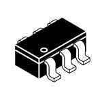
ICGOO电子元器件商城为您提供SMS05CT1G由ON Semiconductor设计生产,在icgoo商城现货销售,并且可以通过原厂、代理商等渠道进行代购。 SMS05CT1G价格参考。ON SemiconductorSMS05CT1G封装/规格:TVS - 二极管, 14.5V Clamp 24A (8/20µs) Ipp Tvs Diode Surface Mount 6-TSOP。您可以下载SMS05CT1G参考资料、Datasheet数据手册功能说明书,资料中有SMS05CT1G 详细功能的应用电路图电压和使用方法及教程。
ON Semiconductor的SMS05CT1G是一款瞬态电压抑制(TVS)二极管,属于低电容双向保护器件,主要用于电子电路中的静电放电(ESD)和瞬态电压保护。其典型应用场景包括:

1. 便携式电子设备:广泛应用于智能手机、平板电脑、笔记本电脑等设备的数据接口(如USB、HDMI、音频接口),防止人体静电或连接过程中产生的瞬态电压损坏敏感元件。

2. 通信接口保护:适用于RS-232、以太网端口、SIM卡接口等,提供快速响应的过压保护,确保信号完整性的同时提升系统可靠性。

3. 消费类电子产品:用于数码相机、MP3播放器、可穿戴设备等人机交互频繁的产品中,保护I/O端口免受日常使用中的ESD冲击。

4. 工业控制与汽车电子辅助系统:在非动力系统的低压控制电路中(如车载信息娱乐系统、传感器接口),提供稳定可靠的瞬态保护。

SMS05CT1G具有低工作电压(反向关断电压5V)、高通流能力、响应速度快(皮秒级)和小封装(SOD-323)等特点,适合空间受限且对防护性能要求高的应用。其低电容特性(典型值15pF)确保了对高速信号传输的影响最小,是高速数据线路的理想保护元件。
| 参数 | 数值 |
| 产品目录 | |
| 描述 | TVS DIODE 5VWM 14.5VC 6TSOPTVS二极管阵列 5 Line TVS Array |
| 产品分类 | |
| 品牌 | ON Semiconductor |
| 产品手册 | |
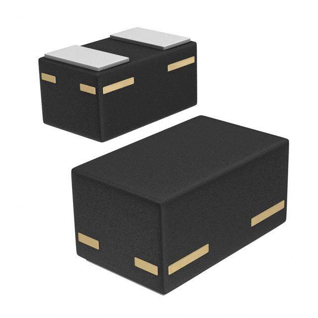
| 产品图片 |
|
| rohs | 符合RoHS无铅 / 符合限制有害物质指令(RoHS)规范要求 |
| 产品系列 | 二极管与整流器,TVS二极管,TVS二极管阵列,ON Semiconductor SMS05CT1G- |
| 数据手册 | |
| 产品型号 | SMS05CT1G |
| 不同频率时的电容 | 260pF @ 1MHz |
| 产品种类 | TVS二极管阵列 |
| 供应商器件封装 | 6-TSOP |
| 其它名称 | SMS05CT1GOSCT |
| 击穿电压 | 6.2 V |
| 功率-峰值脉冲 | 350W |
| 包装 | 剪切带 (CT) |
| 单向通道 | 5 |
| 双向通道 | - |
| 商标 | ON Semiconductor |
| 安装类型 | 表面贴装 |
| 安装风格 | SMD/SMT |
| 封装 | Reel |
| 封装/外壳 | SC-74,SOT-457 |
| 封装/箱体 | TSOP-6 |
| 尺寸 | 1.5 mm W x 3 mm L |
| 峰值浪涌电流 | 24 A |
| 峰值脉冲功率耗散 | 350 W |
| 工作温度 | -40°C ~ 125°C (TJ) |
| 工作电压 | 5 V |
| 工厂包装数量 | 3000 |
| 应用 | 通用 |
| 最大工作温度 | + 125 C |
| 最小工作温度 | - 40 C |
| 极性 | Unidirectional |
| 标准包装 | 1 |
| 电压-击穿(最小值) | 6.2V |
| 电压-反向关态(典型值) | 5V(最小值) |
| 电压-箝位(最大值)@Ipp | 14.5V |
| 电容 | 260 pF |
| 电流-峰值脉冲(10/1000µs) | 24A (8/20µs) |
| 电源线路保护 | 无 |
| 端接类型 | SMD/SMT |
| 类型 | 齐纳 |
| 系列 | SMSxxC |
| 通道 | 5 Channels |
| 钳位电压 | 14.5 V |


PDF Datasheet 数据手册内容提取
SMS05C, SMS12C, SMS15C, SMS24C ESD Protection Diode Array, 5-Line This 5−line surge protection array is designed for application requiring transient voltage protection capability. It is intended for use wwwwww..oonnsseemmii..ccoomm in over−transient voltage and ESD sensitive equipment such as computers, printers, automotive electronics, networking TSOP−6 FIVE SURGE communication and other applications. This device features a PROTECTION monolithic common anode design which protects five independent 350 W PEAK POWER lines in a single TSOP−6 package. PIN ASSIGNMENT Features • Protects up to 5 Lines in a Single TSOP−6 Package • Peak Power Dissipation − 350 W (8 (cid:2) 20 (cid:2)s Waveform) 1 6 • ESD Rating of Class 3B (Exceeding 8.0 kV) per Human Body Model 6 2 5 and Class C (Exceeding 400 V) per Machine Model • 1 3 4 Compliance with IEC 61000−4−2 (ESD) 15 kV (Air), 8.0 kV TSOP−6 (Contact) CASE 318G PIN 1.CATHODE • Flammability Rating of UL 94 V−0 SCALE 2:1 2.ANODE • 3.CATHODE These are Pb−Free Devices 4.CATHODE 5.CATHODE Applications 6.CATHODE • Hand−Held Portable Applications • MARKING DIAGRAM Networking and Telecom • Automotive Electronics • Serial and Parallel Ports 6x M(cid:2) • (cid:2) Notebooks, Desktops, Servers MAXIMUM RATINGS (TJ = 25°C unless otherwise specified) x = SMS05C:J Symbol Rating Value Unit = SMS12C:K = SMS15C:L PPK 1 Peak Power Dissipation 350 W = SMS24C:M 8 (cid:2) 20 (cid:2)s Double Exponential Waveform M = Date Code (Note 1) (cid:2) = Pb−Free Package T Operating Junction Temperature Range −40 to 150 °C (Note: Microdot may be in either location) J TSTG Storage Temperature Range −55 to 150 °C TL Lead Solder Temperature (10 s) 260 °C ORDERING INFORMATION ESD Human Body Model ( HBM) >8000 V Device Package Shipping† Machine Model (MM) >400 IEC 61000−4−2 Air (ESD) >15000 SMS05CT1G IEC 61000−4−2 Contact (ESD) >8000 Stresses exceeding those listed in the Maximum Ratings table may damage the SMS12CT1G TSOP−6 3000/Tape & Reel device. If any of these limits are exceeded, device functionality should not be (Pb−Free) SMS15CT1G assumed, damage may occur and reliability may be affected. 1. Non−repetitive current pulse per Figure 3. SMS24CT1G †For information on tape and reel specifications, including part orientation and tape sizes, please refer to our Tape and Reel Packaging Specification Brochure, BRD8011/D. © Semiconductor Components Industries, LLC, 2011 1 Publication Order Number: November, 2017 − Rev. 8 SMS05C/D
SMS05C, SMS12C, SMS15C, SMS24C SMS05C ELECTRICAL CHARACTERISTICS (TJ = 25°C unless otherwise specified) Parameter Symbol Conditions Min Typ Max Unit Reverse Working Voltage VRWM (Note 2) 5.0 V Breakdown Voltage VBR IT = 1.0 mA (Note 3) 6.2 7.2 V Reverse Leakage Current IR VRWM = 5.0 V 5.0 (cid:2)A Clamping Voltage VC IPP = 5.0 A (8 (cid:2) 20 (cid:2)s Waveform) 9.8 V Clamping Voltage VC IPP = 24 A (8 (cid:2) 20 (cid:2)s Waveform) 14.5 V Maximum Peak Pulse Current IPP 8 (cid:2) 20 (cid:2)s Waveform 24 A Capacitance CJ VR = 0 V, f = 1.0 MHz (Line to GND) 260 400 pF SMS12C ELECTRICAL CHARACTERISTICS (TJ = 25°C unless otherwise specified) Parameter Symbol Conditions Min Typ Max Unit Reverse Working Voltage VRWM (Note 2) 12 V Breakdown Voltage VBR IT = 1.0 mA (Note 3) 13.3 15 V Reverse Leakage Current IR VRWM = 12 V 0.001 1.0 (cid:2)A Clamping Voltage VC IPP = 5.0 A (8 (cid:2) 20 (cid:2)s Waveform) 19 V Clamping Voltage VC IPP = 15 A (8 (cid:2) 20 (cid:2)s Waveform) 23 V Maximum Peak Pulse Current IPP 8 (cid:2) 20 (cid:2)s Waveform 15 A Capacitance CJ VR = 0 V, f = 1.0 MHz (Line to GND) 120 150 pF SMS15C ELECTRICAL CHARACTERISTICS (TJ = 25°C, unless otherwise specified) (See Note 4) Parameter Symbol Conditions Min Typ Max Unit Reverse Working Voltage VRWM (Note 2) 15 V Breakdown Voltage VBR IT = 1.0 mA (Note 3) 17 19 V Reverse Leakage Current IR VRWM = 15 V 0.05 1.0 (cid:2)A Clamping Voltage VC IPP = 5.0 A (8 (cid:2) 20 (cid:2)s Waveform) 24 V Clamping Voltage VC IPP = 12 A (8 (cid:2) 20 (cid:2)s Waveform) 29 V Maximum Peak Pulse Current IPP 8 (cid:2) 20 (cid:2)s Waveform 12 A Capacitance CJ VR = 0 V, f = 1.0 MHz (Line to GND) 95 125 pF SMS24C ELECTRICAL CHARACTERISTICS (TJ = 25°C, unless otherwise specified) Parameter Symbol Conditions Min Typ Max Unit Reverse Working Voltage VRWM (Note 2) 24 V Breakdown Voltage VBR IT = 1.0 mA (Note 3) 26.7 32 V Reverse Leakage Current IR VRWM = 24 V 0.001 1.0 (cid:2)A Clamping Voltage VC IPP = 5.0 A (8 (cid:2) 20 (cid:2)s Waveform) 40 V Clamping Voltage VC IPP = 8 A (8 (cid:2) 20 (cid:2)s Waveform) 44 V Maximum Peak Pulse Current IPP 8 (cid:2) 20 (cid:2)s Waveform 8.0 A Capacitance CJ VR = 0 V, f = 1.0 MHz (Line to GND) 60 75 pF 2. Surge protection devices are normally selected according to the working peak reverse voltage (VRWM), which should be equal or greater than the DC or continuous peak operating voltage level. 3. VBR is measured at pulse test current IT. 4. Parametrics are the same for the Pb−Free packages, which are suffixed with a “G’’. www.onsemi.com 2
SMS05C, SMS12C, SMS15C, SMS24C TYPICAL PERFORMANCE CURVES (TJ = 25°C unless otherwise specified) OWER 19000 T19000 tr PEAK VALUE IRSM @ 8 (cid:2)s K P 80 EN 80 PULSE WIDTH (tP) IS DEFINED NG IN % OF PEA°C= 25NT @ TA 765000 PULSE CURR 765000 HAAPLSEF A TVKAH LACUTU ERP OIRREISNNMT/T2 W D@HE EC2R0A EY(cid:2) s=T H8E (cid:2)s E DERATIR CURRE 4300 F PEAK 4300 tP SO 20 O 20 UL % K P 10 10 A E 0 0 P 0 25 50 75 100 125 150 175 200 0 20 40 60 80 TA, AMBIENT TEMPERATURE (°C) t, TIME ((cid:2)s) Figure 1. Pulse Derating Curve Figure 2. 8 × 20 (cid:2)s Pulse Waveform 50 300 SMS24C 8 x 20 (cid:2)s f = 1.0 MHz V) 45 PULSE WAVEFORM pF)250 E ( 40 E ( G C A 35 N T SMS15C A200 VOL 30 SMS12C CIT SMS05C G 25 PA150 N A MPI 20 N C CLA 15 SMS05C CTIO100 , C 10 N SMS12C V U 50 5 J SMS15C SMS24C 0 0 0 5 10 15 20 25 0 5 10 15 20 25 IPP, PEAK PULSE CURRENT (A) VBR, REVERSE VOLTAGE (V) Figure 3. Clamping Voltage vs. Peak Pulse Current Figure 4. Junction Capacitance vs. Reverse Voltage Figure 5. ESD Pulse IEC 61000−4−2 Figure 6. SMS15CT1 ESD Response for IEC (8.0 kV Contact) 61000−4−2 (+8.0 kV Contact) www.onsemi.com 3
SMS05C, SMS12C, SMS15C, SMS24C TYPICAL COMMON ANODE APPLICATIONS A 5 surge protection junction common anode design in a especially when board space is at a premium. A simplified TSOP−6 package protects four separate lines using only one example of SMS05C Series Device applications is package. This adds flexibility and creativity to PCB design illustrated below. A KEYBOARD B TERMINAL FUNCTIONAL I/O C PRINTER DECODER D ETC. E GND SMS05C SERIES DEVICE Figure 7. Computer Interface Protection VDD VGG ADDRESS BUS RAM ROM DATA BUS CPU I/O CLOCK CONTROL BUS GND SMS05C SERIES DEVICE Figure 8. Microprocessor Protection www.onsemi.com 4
SMS05C, SMS12C, SMS15C, SMS24C PACKAGE DIMENSIONS TSOP−6 CASE 318G−02 ISSUE V D NOTES: 1. DIMENSIONING AND TOLERANCING PER ASME Y14.5M, 1994. H 2. CONTROLLING DIMENSION: MILLIMETERS. 3. MAXIMUM LEAD THICKNESS INCLUDES LEAD FINISH. MINIMUM LEAD THICKNESS IS THE MINIMUM THICKNESS OF BASE MATERIAL. É6 É5 4 L2 4. DIMENSIONS D AND E1 DO NOT INCLUDE MOLD FLASH, GAUGE PROTRUSIONS, OR GATE BURRS. MOLD FLASH, PROTRUSIONS, OR E1 E PLANE GATE BURRS SHALL NOT EXCEED 0.15 PER SIDE. DIMENSIONS D ÉÉ AND E1 ARE DETERMINED AT DATUM H. 1 2 3 5. PIN ONE INDICATOR MUST BE LOCATED IN THE INDICATED ZONE. L NOTE 5 b M C PSLEAANTIENG DIM MIN MILLNIMOEMTERSMAX DETAIL Z A 0.90 1.00 1.10 e A1 0.01 0.06 0.10 b 0.25 0.38 0.50 c 0.10 0.18 0.26 c D 2.90 3.00 3.10 0.05 A EE1 21..5300 21..7550 31..0700 e 0.85 0.95 1.05 A1 L 0.20 0.40 0.60 DETAIL Z L2 0.25 BSC M 0(cid:2) − 10(cid:2) RECOMMENDED SOLDERING FOOTPRINT* 6X 0.60 3.20 6X 0.95 0.95 PITCH DIMENSIONS: MILLIMETERS *For additional information on our Pb−Free strategy and soldering details, please download the ON Semiconductor Soldering and Mounting Techniques Reference Manual, SOLDERRM/D. ON Semiconductor and are trademarks of Semiconductor Components Industries, LLC dba ON Semiconductor or its subsidiaries in the United States and/or other countries. ON Semiconductor owns the rights to a number of patents, trademarks, copyrights, trade secrets, and other intellectual property. A listing of ON Semiconductor’s product/patent coverage may be accessed at www.onsemi.com/site/pdf/Patent−Marking.pdf. ON Semiconductor reserves the right to make changes without further notice to any products herein. ON Semiconductor makes no warranty, representation or guarantee regarding the suitability of its products for any particular purpose, nor does ON Semiconductor assume any liability arising out of the application or use of any product or circuit, and specifically disclaims any and all liability, including without limitation special, consequential or incidental damages. Buyer is responsible for its products and applications using ON Semiconductor products, including compliance with all laws, regulations and safety requirements or standards, regardless of any support or applications information provided by ON Semiconductor. “Typical” parameters which may be provided in ON Semiconductor data sheets and/or specifications can and do vary in different applications and actual performance may vary over time. All operating parameters, including “Typicals” must be validated for each customer application by customer’s technical experts. ON Semiconductor does not convey any license under its patent rights nor the rights of others. ON Semiconductor products are not designed, intended, or authorized for use as a critical component in life support systems or any FDA Class 3 medical devices or medical devices with a same or similar classification in a foreign jurisdiction or any devices intended for implantation in the human body. Should Buyer purchase or use ON Semiconductor products for any such unintended or unauthorized application, Buyer shall indemnify and hold ON Semiconductor and its officers, employees, subsidiaries, affiliates, and distributors harmless against all claims, costs, damages, and expenses, and reasonable attorney fees arising out of, directly or indirectly, any claim of personal injury or death associated with such unintended or unauthorized use, even if such claim alleges that ON Semiconductor was negligent regarding the design or manufacture of the part. ON Semiconductor is an Equal Opportunity/Affirmative Action Employer. This literature is subject to all applicable copyright laws and is not for resale in any manner. PUBLICATION ORDERING INFORMATION LITERATURE FULFILLMENT: N. American Technical Support: 800−282−9855 Toll Free ON Semiconductor Website: www.onsemi.com Literature Distribution Center for ON Semiconductor USA/Canada 19521 E. 32nd Pkwy, Aurora, Colorado 80011 USA Europe, Middle East and Africa Technical Support: Order Literature: http://www.onsemi.com/orderlit Phone: 303−675−2175 or 800−344−3860 Toll Free USA/Canada Phone: 421 33 790 2910 Fax: 303−675−2176 or 800−344−3867 Toll Free USA/Canada Japan Customer Focus Center For additional information, please contact your local Email: orderlit@onsemi.com Phone: 81−3−5817−1050 Sales Representative ◊ www.onsemi.com SMS05C/D 5
Mouser Electronics Authorized Distributor Click to View Pricing, Inventory, Delivery & Lifecycle Information: O N Semiconductor: SMS05CT1G SMS12CT1G SMS15CT1G SMS24CT1G