 Datasheet下载
- 型号: CDSOD323-T12C
- 制造商: Bourns
- 库位|库存: xxxx|xxxx
- 要求:
| 数量阶梯 | 香港交货 | 国内含税 |
| +xxxx | $xxxx | ¥xxxx |
查看当月历史价格
查看今年历史价格
CDSOD323-T12C产品简介:
ICGOO电子元器件商城为您提供CDSOD323-T12C由Bourns设计生产,在icgoo商城现货销售,并且可以通过原厂、代理商等渠道进行代购。 CDSOD323-T12C价格参考¥2.51-¥3.24。BournsCDSOD323-T12C封装/规格:TVS - 二极管, 28.3V (Typ) Clamp 11A (8/20µs) Ipp Tvs Diode Surface Mount SOD-323。您可以下载CDSOD323-T12C参考资料、Datasheet数据手册功能说明书,资料中有CDSOD323-T12C 详细功能的应用电路图电压和使用方法及教程。
Bourns Inc. 的 CDSOD323-T12C 是一款瞬态电压抑制(TVS)二极管,属于表面贴装的小型化保护器件,主要用于电子电路中的过电压和静电放电(ESD)防护。该型号采用紧凑的SOD-323封装,适用于空间受限的便携式设备。

其典型应用场景包括:
1. 通信接口保护:广泛用于USB、HDMI、RS-232、以太网等高速数据线路,防止因雷击感应、电源突波或静电放电造成的损坏。
2. 消费类电子产品:应用于智能手机、平板电脑、笔记本电脑及可穿戴设备中,保护敏感的集成电路免受日常使用中的ESD冲击(如人体接触产生的静电)。
3. 工业控制设备:用于PLC、传感器、人机界面等设备的数据端口和电源引脚,提升系统在恶劣电磁环境下的可靠性。
4. 汽车电子:适合车载信息娱乐系统、导航设备和辅助驾驶模块中的信号线保护,满足车规级稳定性和耐温要求。

CDSOD323-T12C 具有低电容特性(通常低于1pF),确保对高速信号传输影响极小;同时具备快速响应时间(皮秒级)和高浪涌吸收能力,能有效钳制瞬态电压至安全水平。其工作电压为12V,适合用于12V或以下的直流电路保护。

综上,该器件适用于需要高效、紧凑型过压保护的各类电子系统,尤其在高速信号线和便携设备中表现优异。
| 参数 | 数值 |
| 产品目录 | |
| 描述 | TVS DIODE 12VWM 19VC SOD323TVS 二极管 - 瞬态电压抑制器 TVS Diode 12VOLT |
| 产品分类 | |
| 品牌 | Bourns |
| 产品手册 | |
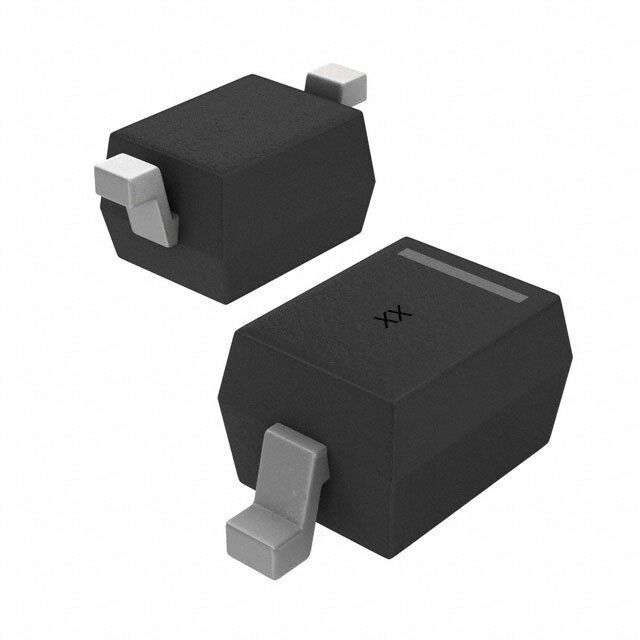
| 产品图片 |
|
| rohs | 符合RoHS无铅 / 符合限制有害物质指令(RoHS)规范要求 |
| 产品系列 | 二极管与整流器,TVS二极管,TVS 二极管 - 瞬态电压抑制器,Bourns CDSOD323-T12C- |
| 数据手册 | |
| 产品型号 | CDSOD323-T12C |
| 不同频率时的电容 | 3pF @ 1MHz |
| 产品种类 | TVS 二极管 - 瞬态电压抑制器 |
| 供应商器件封装 | SOD-323 |
| 其它名称 | CDSOD323-T12CDKR |
| 击穿电压 | 13.3 V |
| 功率-峰值脉冲 | 350W |
| 包装 | Digi-Reel® |
| 单向通道 | - |
| 双向通道 | 1 |
| 商标 | Bourns |
| 安装类型 | 表面贴装 |
| 安装风格 | SMD/SMT |
| 封装 | Reel |
| 封装/外壳 | SC-76,SOD-323 |
| 封装/箱体 | SOD-323 |
| 尺寸 | 1.45 mm W x 1.9 mm L x 1 mm H |
| 峰值浪涌电流 | 11 A |
| 峰值脉冲功率耗散 | 350 W |
| 工作温度 | -55°C ~ 150°C (TJ) |
| 工作电压 | 12 V |
| 工厂包装数量 | 3000 |
| 应用 | 通用 |
| 最大工作温度 | + 150 C |
| 最小工作温度 | - 55 C |
| 极性 | Bidirectional |
| 标准包装 | 1 |
| 电压-击穿(最小值) | 13.3V |
| 电压-反向关态(典型值) | 12V |
| 电压-箝位(最大值)@Ipp | 19V |
| 电容 | 3 pF |
| 电流-峰值脉冲(10/1000µs) | 11A (8/20µs) |
| 电源线路保护 | 无 |
| 端接类型 | SMD/SMT |
| 类型 | 齐纳 |
| 钳位电压 | 19 V |
| 零件号别名 | CDS0D323-T12C |


- 商务部:美国ITC正式对集成电路等产品启动337调查
- 曝三星4nm工艺存在良率问题 高通将骁龙8 Gen1或转产台积电
- 太阳诱电将投资9.5亿元在常州建新厂生产MLCC 预计2023年完工
- 英特尔发布欧洲新工厂建设计划 深化IDM 2.0 战略
- 台积电先进制程称霸业界 有大客户加持明年业绩稳了
- 达到5530亿美元!SIA预计今年全球半导体销售额将创下新高
- 英特尔拟将自动驾驶子公司Mobileye上市 估值或超500亿美元
- 三星加码芯片和SET,合并消费电子和移动部门,撤换高东真等 CEO
- 三星电子宣布重大人事变动 还合并消费电子和移动部门
- 海关总署:前11个月进口集成电路产品价值2.52万亿元 增长14.8%


PDF Datasheet 数据手册内容提取
NT *RoHS VCEOARVMSIAPILOLINAASB LE Features Applications NT MPLIA n RoHS compliant* n Cellular phones O HS C n Protects one line or one I/O port n PDAs and notebooks *Ro n Bidirectional configuration n Digital cameras n ESD protection 30 kV max. n MP3 players and GPS n Low capacitance: ~3 pF typical n USB interface n Replaces 0805 MLV devices REE D F LEA CDSOD323-TxxC - TVS Diode Array Series General Information PtBhooeru tsranebsmle oi ccffooenmrdsm uTcurtanonirc sianietdinoutn sVstro,y lc ttaoogm depe Suvtueinplogpp ra einnsdcs roverLiVa dEAEAseRDHr SioISrnF OaR CgNeEOySEl qyM AdP uRLsIiE ioAmpNdmTa*eleslen frto emr lseaucnrtugrofean caictnu cdroe EmrsSp aDor nepe rconhttesa.clletionng ing UNIDIRE1CTIONAL BIDIREC1TIONAL applications, in SOD323 package size formaRto. The Transient Voltage Supressor Array series offers a choice of voltage types ranging from 3 V to 24 V in a unidirectional or bidirectional configuration. Bourns® Chip Diodes conform to JEDEC standards, are easy to handle on standard pick and place equipment and their flat configuration minimizes roll away. The Bourns® device will assist compliance with IEC 61000-4-2 (ESD), IEC 61000-4-4 (EFT) and IEC 61000-4-5 (Surge) requirements. 2 2 Note: For 12 V and 24 V VDSL applications, the CDSOD323-TxxC-DSL family of devices is recommended. Electrical & Thermal Characteristics (@ TA = 25 °C Unless Otherwise Noted) Parameter Symbol Value Unit Peak Pulse Power (tp = 8/20 µs) PPP 350 W Operating Temperature TJ -55 to +150 °C Storage Temperature TSTG -55 to +150 °C CDSOD323- Parameter Symbol Uni- Bi- Uni- Bi- Uni- Bi- Uni- Bi- Unit T03 T03C T05 T05C T08 T08C T12 T12C Minimum Breakdown Voltage @ 1 mA VBR 4.0 6.0 8.5 13.3 V Working Peak Voltage VWM 3.3 5.0 8.0 12.0 V Maximum Clamping Voltage @ IP = 1 A VC 7.0 9.8 13.4 19.0 V Typical Clamping Voltage 19.0 V 18.3 V 18.5 V 28.3 V @ 8/20 µs @ IPP VC @ 20 A @ 17 A @ 17 A @ 11 A V Maximum Leakage Current @ VWM ID 5 5 2 1 µA Typical Capacitance @ 0 V, 1 MHz CJ 3 pF CDSOD323- Parameter Symbol Uni- Bi- Uni- Bi- Uni- Bi- Unit T15 T15C T18 T18C T24 T24C Minimum Breakdown Voltage @ 1 mA VBR 16.7 20.0 26.7 V Working Peak Voltage VWM 15.0 18.0 24.0 V Maximum Clamping Voltage @ IP = 1 A VC 24.0 29.0 43.0 V Typical Clamping Voltage 31.8 V 45.0 V 56.0 V @ 8/20 µs @ IPP VC @ 10 A @ 8 A @ 6 A V Maximum Leakage Current @ VWM ID 1 µA Typical Capacitance @ 0 V, 1 MHz CJ 3 pF Notes: 1. Part numbers with suffix “C” indicate bidirectional device, i.e. CDSOD323-T05C. 2. For bidirectional devices only, the electrical specifications apply in both directions. *RoHS Directive 2002/95/EC Jan. 27, 2003 including annex and RoHS Recast 2011/65/EU June 8, 2011. Specifications are subject to change without notice. The device characteristics and parameters in this data sheet can and do vary in different applications and actual device performance may vary over time. Users should verify actual device performance in their specific applications.
CDSOD323-TxxC - TVS Diode Array Series CATHODE BAND C (FOR UNIDIRECTIONAL PRODUCTS ONLY) A Product DimensionsE Recommended Footprint This is an RoHS compliant molded JEDEC SOD-323B package with W 100 % Sn plating on the terminations. It weighs approximately 30 mg and has a flammability rating of UL 94V-0. L S L CATHODE BAND F C D H (FOR UNIDIRECTIONAL PRODUCTS ONLY) A E J Dimensions (Nominal) B W 0.80 L (0.031) 1.40 L S S L F D H (0.055) 0.50 W J (0.020) MM DIMENSIONS: Dimensions (INCHES) 1.60 - 1.90 A (0.063 - 0.075) Typical Part Marking B 1.15 - 1.45 Each device has device marking outlined below and the (0.045 - 0.057) unidirectional devices have an additional Polarity Band indicating the cathode. 2.39 - 2.70 C (0.094 - 0.106) CDSOD323-T03 ............................................................................3 0.92 - 1.14 CDSOD323-T03C..........................................................................3C D (0.036 - 0.045) CDSOD323-T05 ............................................................................5 CDSOD323-T05C..........................................................................5C 0.25 - 0.40 E CDSOD323-T08 ............................................................................8 (0.010 - 0.016) CDSOD323-T08C..........................................................................8C 0.08 - 0.20 CDSOD323-T12 ............................................................................2 F (0.003 - 0.008) CDSOD323-T12C..........................................................................2C CDSOD323-T15 ............................................................................6 H 0.13 MAX. CDSOD323-T15C..........................................................................6C (0.005) ......... CDSOD323-T18 ............................................................................1 CDSOD323-T18C..........................................................................1C 0.30 - 0.45 J CDSOD323-T24 ............................................................................4 (0.012 - 0.018) CDSOD323-T24C..........................................................................4C MM DIMENSIONS: (INCHES) Environmental Specifications Moisture Sensitivity Level ................................................................1 ESD Classification (HBM).............................................................3B Specifications are subject to change without notice. The device characteristics and parameters in this data sheet can and do vary in different applications and actual device performance may vary over time. Users should verify actual device performance in their specific applications.
CDSOD323-TxxC - TVS Diode Array Series Performance Graphs Peak Pulse Power vs Pulse Time Pulse Waveform 10,000 120 nt (W) % of I)PP 100 tt tTttd e ==s t82 W 0µ saµvseform Parameters urre 1,000 350 W, 8/20 µs Waveform nt ( 80 et C e Pulse e Curr 60 – Peak 100 ak Puls 40 td = t|IPP/2 P PP – Pe 20 10 I PP 0 0.1 1 10 100 1,000 10,000 0 5 10 15 20 25 30 td – Pulse Duration (µs) t – Time (µs) Block Diagram How to Order UNIDIRECTIONAL BIDIRECTIONAL CD SOD323 - T 05 C 1 1 Common Code Chip Diode Package SOD323 = SOD-323 Package Model T = Transient Voltage Suppressor Working Peak Reverse Voltage 05 = 5 VWM (Volts) Suffix 2 2 C = Bidirectional Diode Specifications are subject to change without notice. The device characteristics and parameters in this data sheet can and do vary in different applications and actual device performance may vary over time. Users should verify actual device performance in their specific applications.
CDSOD323-TxxC - TVS Diode Array Series Packaging Information The product is packaged in tape and reel format per EIA-481 standard. P 0 d P1 E T Index Hole 120 ° F D2 W B D1 D P A C Product Trailer Orientation Device Leader ....... ....... ....... ....... W1 End ....... ....... ....... ....... Start MM DIMENSIONS: 10 pitches (min.) 10 pitches (min.) (INCHES) Direction of Feed Item Symbol SOD-323 1.55 ± 0.10 Carrier Width A (0.061 ± 0.004) 2.90 ± 0.10 Carrier Length B (0.114 ± 0.004) 1.35 ± 0.10 Carrier Depth C (0.053 ± 0.004) 1.55 ± 0.05 Sprocket Hole d (0.061 ± 0.002) 178 Reel Outside Diameter D (7.008) 80.0 Reel Inner Diameter D1 (3.150) MIN. Asia-Pacific: 13.0 ± 0.20 Tel: +886-2 2562-4117 Feed Hole Diameter D2 (0.512 ± 0.008) Email: asiacus@bourns.com Sprocket Hole Position E 1.75 ± 0.10 Europe: (0.069 ± 0.004) Tel: +36 88 520 390 Punch Hole Position F 3.50 ± 0.05 Email: eurocus@bourns.com (0.138 ± 0.002) The Americas: 4.00 ± 0.10 Punch Hole Pitch P Tel: +1-951 781-5500 (0.157 ± 0.004) Email: americus@bourns.com 4.00 ± 0.10 Sprocket Hole Pitch P0 (0.157 ± 0.004) www.bourns.com 2.00 ± 0.05 Embossment Center P1 (0.079 ± 0.002) 0.20 ± 0.10 Overall Tape Thickness T (0.008 ± 0.004) 8.00 ± 0.20 Tape Width W (0.315 ± 0.008) 13.5 Reel Width W1 (0.531) MAX. Quantity per Reel -- 3000 REV. 01/18 Specifications are subject to change without notice. The device characteristics and parameters in this data sheet can and do vary in different applications and actual device performance may vary over time. Users should verify actual device performance in their specific applications.