ICGOO在线商城 > SMM4F18A-TR

 Datasheet下载
- 型号: SMM4F18A-TR
- 制造商: STMicroelectronics
- 库位|库存: xxxx|xxxx
- 要求:
| 数量阶梯 | 香港交货 | 国内含税 |
| +xxxx | $xxxx | ¥xxxx |
查看当月历史价格
查看今年历史价格
SMM4F18A-TR产品简介:
ICGOO电子元器件商城为您提供SMM4F18A-TR由STMicroelectronics设计生产,在icgoo商城现货销售,并且可以通过原厂、代理商等渠道进行代购。 提供SMM4F18A-TR价格参考¥询价-¥询价以及STMicroelectronicsSMM4F18A-TR封装/规格参数等产品信息。 你可以下载SMM4F18A-TR参考资料、Datasheet数据手册功能说明书, 资料中有SMM4F18A-TR详细功能的应用电路图电压和使用方法及教程。
| 参数 | 数值 |
| 产品目录 | |
| 描述 | TVS DIODE 18VWM 39.3VC DO222AATVS 二极管 - 瞬态电压抑制器 Hi Temp Transil Diode |
| 产品分类 | |
| 品牌 | STMicroelectronics |
| 产品手册 | |
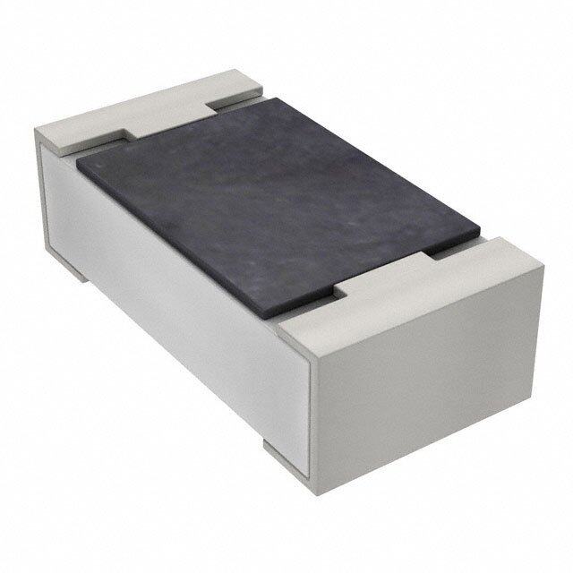
| 产品图片 |
|
| rohs | 符合RoHS无铅 / 符合限制有害物质指令(RoHS)规范要求 |
| 产品系列 | 二极管与整流器,TVS二极管,TVS 二极管 - 瞬态电压抑制器,STMicroelectronics SMM4F18A-TRSMM4F, TRANSIL™ |
| 数据手册 | |
| 产品型号 | SMM4F18A-TR |
| 不同频率时的电容 | - |
| 产品目录页面 | |
| 产品种类 | TVS 二极管 - 瞬态电压抑制器 |
| 供应商器件封装 | DO222-AA |
| 其它名称 | 497-7905-2 |
| 其它有关文件 | http://www.st.com/web/catalog/sense_power/FM114/CL1460/SC1888/PF204614?referrer=70071840http://www.st.com/web/catalog/sense_power/FM114/CL1460/SC233/PF204614?referrer=70071840 |
| 击穿电压 | 20.9 V |
| 功率-峰值脉冲 | 400W |
| 包装 | 带卷 (TR) |
| 单向通道 | 1 |
| 双向通道 | - |
| 商标 | STMicroelectronics |
| 商标名 | Transil |
| 安装类型 | 表面贴装 |
| 安装风格 | SMD/SMT |
| 封装 | Reel |
| 封装/外壳 | DO-222AA |
| 封装/箱体 | DO-222AA |
| 尺寸 | 1.9 mm W x 2.95 mm L |
| 峰值浪涌电流 | 59 A |
| 峰值脉冲功率耗散 | 400 W |
| 工作温度 | -55°C ~ 175°C (TJ) |
| 工作电压 | 18 V |
| 工厂包装数量 | 12000 |
| 应用 | 通用 |
| 最大工作温度 | + 175 C |
| 最小工作温度 | - 55 C |
| 极性 | Unidirectional |
| 标准包装 | 12,000 |
| 电压-击穿(最小值) | 20.9V |
| 电压-反向关态(典型值) | 18V |
| 电压-箝位(最大值)@Ipp | 39.3V |
| 电流-峰值脉冲(10/1000µs) | 59A (8/20µs) |
| 电源线路保护 | 无 |
| 端接类型 | SMD/SMT |
| 类型 | 齐纳 |
| 系列 | SMM4F |
| 钳位电压 | 39.3 V |


- 商务部:美国ITC正式对集成电路等产品启动337调查
- 曝三星4nm工艺存在良率问题 高通将骁龙8 Gen1或转产台积电
- 太阳诱电将投资9.5亿元在常州建新厂生产MLCC 预计2023年完工
- 英特尔发布欧洲新工厂建设计划 深化IDM 2.0 战略
- 台积电先进制程称霸业界 有大客户加持明年业绩稳了
- 达到5530亿美元!SIA预计今年全球半导体销售额将创下新高
- 英特尔拟将自动驾驶子公司Mobileye上市 估值或超500亿美元
- 三星加码芯片和SET,合并消费电子和移动部门,撤换高东真等 CEO
- 三星电子宣布重大人事变动 还合并消费电子和移动部门
- 海关总署:前11个月进口集成电路产品价值2.52万亿元 增长14.8%


PDF Datasheet 数据手册内容提取
SMM4FxxA 400 W TransilTM Datasheet - production data Description The SMM4F Transil serie has been designed to protect sensitive equipment against electro-static A discharges according to IEC 61000-4-2, MIL STD 883 Method 3015, and electrical over stress such as IEC 61000-4-4 and 5. They are generally for K surges below 400 W 10/1000 μs. STmiteFlat This planar technology makes it compatible with (DO216-AAFlat) high-end equipment and SMPS where low leakage current and high junction temperature are required to provide reliability and stability over time. Their low clamping voltages provide a better safety margin to protect sensitive circuits with extended life time expectancy. Features Packaged in STmite Flat, this minimizes PCB Typical peak pulse power: space consumption (footprint in accordance with 400 W (10/1000 μs) IPC 7531 standard). Transil is a trademark of 2.4 kW (8/20 μs) STMicroelectronics. Stand-off voltage range: from 5 V to 33 V Unidirectional type Low leakage current: 0.2 μA at 25 °C 1 μA at 85 °C Operating T max: 175 °C j JEDEC registered package outline RoHS package Halogen free molding compound Complies with the following standards IEC 61000-4-2 level 4: 15 kV (air discharge) 8 kV (contact discharge) MIL STD 883G-Method 3015-7: class3 25 kV (human body model) January 2017 DocID14250 Rev 4 1/12 This is information on a product in full production. www.st.com
Characteristics SMM4FxxA 1 Characteristics Table 1: Absolute maximum ratings (Tamb = 25 °C) Symbol Parameter Value Unit Peak pulse voltage VPP (IEC 61000-4-2 contact discharge) 30 kV PPP Peak pulse power dissipation Tj initial = Tamb 400 W P Power dissipation on infinite heatsink Tamb = 125 °C 2.5 W Non repetitive surge peak forward current for tp = 10 ms IFSM unidirectional types Tj initial = Tamb 30 A Tstg Storage temperature range -65 to +175 °C Tj Operating junction temperature range -55 to +175 °C TL Maximum lead temperature for soldering during 10 s 260 °C Table 2: Thermal resistances Symbol Parameter Value Unit Rth(j-l) Junction to leads 20 °C/W Rth(j-a) Junction to ambient on PCB with recommended pad layout 250 Figure 1: Electrical characteristics - parameter definitions (Tamb = 25 °C) 2/12 DocID14250 Rev 4
SMM4FxxA Characteristics Table 3: Electrical characteristics - parameter values (Tamb = 25 °C) IRM max. at VRM VBR at IR(1) 1V0/C1L0 a0t0 I PμPs 10R/1D0(20) 0 V8C/L2 0a tμ IsPP RDµ s8(2/2) 0 αT(3) μs Type 25 °C 85 °C Min. Typ. Max. Max. Max. Max. µA V V mA V A Ω V A Ω 10-4/°C SMM4F5.0A 10 50 5.0 6.46 6.80 7.14 10 9.2 43.5 0.047 13.4 179 0.035 5.7 SMM4F6.0A 10 50 6.0 6.65 7.00 7.35 10 10.3 38.8 0.076 13.7 175 0.036 5.9 SMM4F6.5A 10 50 6.5 7.13 7.50 7.88 10 11.2 37.5 0.093 14.5 166 0.039 6.1 SMM4F8.5A 10 50 8.5 9.5 10.0 10.5 1 14.4 27.7 0.141 19.5 140 0.064 7.3 SMM4F10A 0.2 1 10 11.4 12.0 12.6 1 17.0 23.5 0.187 21.7 127 0.071 7.8 SMM4F12A 0.2 1 12 13.3 14.0 14.7 1 19.9 20.1 0.259 25.3 112 0.094 8.3 SMM4F13A 0.2 1 13 14.3 15.0 15.8 1 21.5 18.6 0.309 27.2 106 0.108 8.4 SMM4F15A 0.2 1 15 17.1 18.0 18.9 1 24.4 16.4 0.335 32.5 90 0.150 8.8 SMM4F18A 0.2 1 18 20.9 22.0 23.1 1 29.2 14.0 0.436 39.3 76 0.214 9.2 SMM4F20A 0.2 1 20 22.8 24.0 25.2 1 32.4 12.0 0.600 42.8 70 0.250 9.4 SMM4F24A 0.2 1 24 26.6 28.01 29.4 1 38.9 9.5 1.00 50 61 0.338 9.6 SMM4F26A 0.2 1 26 28.5 30.0 31.5 1 42.1 9.0 1.18 53.5 58 0.380 9.7 SMM4F28A 0.2 1 28 31.4 33.0 34.7 1 45.4 8.0 1.34 59.0 53 0.456 9.8 SMM4F33A 0.2 1 33 37.1 39.0 41.0 1 53.3 7.0 1.76 69.7 45 0.636 10.0 Notes: (1)Pulse test: tp < 50 ms. (2)To calculate maximum clamping voltage at other surge currents, use the following formula: VCLmax = RD x IPP + VBRmax (3)To calculate VBR versus junction temperature, use the following formula: VBR at Tj = VBR @ 25 °C x (1 + αT x (Tj - 25)) Figure 2: Definition of IPP pulse DocID14250 Rev 4 3/12
Characteristics SMM4FxxA 1.1 Characteristics (curves) Figure 3: Peak power dissipation versus initial Figure 4: Peak pulse power versus exponential junction temperature pulse duration (Tj initial = 25 °C) PPP[Tjinitial]/PPP[Tjinitial=25°C] PPP(kW) 1.1 10.0 1.0 Tjinitial=25°C 0.9 0.8 0.7 0.6 1.0 0.5 0.4 0.3 0.2 0.1 Tjinitial (°C) tp(ms) 0.0 0.1 0 25 50 75 100 125 150 175 200 1.0E-03 1.0E-02 1.0E-01 1.0E+00 1.0E+01 Figure 5: Clamping voltage versus peak pulse Figure 6: Junction capacitance versus reverse current (exponential waveform, maximum values) applied voltage I (A) C(pF) 1000 PP 10000 F=1MHz SMM4F5.0A SMM4F15A Tjinitial=25°C VOSCT=j=3205m°CVRMS 100 SMM4F24A SMM4F33A 1000 SMM4F5.0A 10 SMM4F15A SMM4F24A 100 SMM4F33A 1 tp=8/20µs tp=10/1000µs VR(V) VCL(V) 0.1 10 0 5 10 15 20 25 30 35 40 45 50 55 60 65 70 1 10 100 Figure 7: Peak forward voltage drop versus peak Figure 8: Relative variation of thermal impedance forward current junction to ambient versus pulse duration (printed circuit board FR4, SCu = 1 cm2) IFM(A) Zth(j-a)/Rth(j-a) 1.0E+02 1.00 Onrecommendedpad layout 1.0E+01 0.10 Tj=125°C 1.0E+00 0.01 1.0E-01 Tj=25°C VFM(V) tp(S) 1.0E-02 0.00 0.0 0.5 1.0 1.5 2.0 2.5 3.0 1.0E-03 1.0E-02 1.0E-01 1.0E+00 1.0E+01 1.0E+02 1.0E+03 4/12 DocID14250 Rev 4
SMM4FxxA Characteristics Figure 10: Leakage current versus junction Figure 9: Thermal resistance junction to ambient temperature (typical values) versus copper surface under each lead (printed circuit board FR4, eCu = 35 μm) Rth(j-a)(°C/W) 1.E+04 IR(nA) 200 180 1.E+03 160 VBR≤11.7V 140 1.E+02 120 V >11.7V 1.E+01 BR 100 80 1.E+00 60 SCU(cm²) Tj(°C) VR=VRM 40 1.E-01 0.0 0.2 0.4 0.6 0.8 1.0 1.2 1.4 1.6 1.8 2.0 2.2 25 50 75 100 125 150 175 DocID14250 Rev 4 5/12
Package information SMM4FxxA 2 Package information In order to meet environmental requirements, ST offers these devices in different grades of ECOPACK® packages, depending on their level of environmental compliance. ECOPACK® specifications, grade definitions and product status are available at: www.st.com. ECOPACK® is an ST trademark. Case: JEDEC DO216-AA Flat molded plastic over planar junction Terminals: solder plated, solderable per MIL-STD-750, method 2026 Polarity: for unidirectional types the band indicates cathode. Flammability: epoxy is rated UL94V-0 RoHS package 6/12 DocID14250 Rev 4
SMM4FxxA Package information 2.1 STmite Flat package information Figure 11: STmite Flat package outline Table 4: STmite Flat mechanical data Dimensions Ref. Millimeters Inches Min. Typ. Max. Min. Typ. Max. A 0.80 0.85 0.95 0.031 0.033 0.037 b 0.40 0.55 0.65 0.016 0.022 0.026 b2 0.70 0.85 1.00 0.027 0.033 0.039 c 0.10 0.15 0.25 0.004 0.006 0.009 D 1.75 1.90 2.05 0.069 0.075 0.081 E 3.60 3.80 3.90 0.142 0.150 0.154 E1 2.80 2.95 3.10 0.110 0.116 0.122 L 0.50 0.55 0.80 0.020 0.022 0.031 L1 2.10 2.40 2.60 0.083 0.094 0.102 L2 0.45 0.60 0.75 0.018 0.024 0.030 L3 0.20 0.35 0.50 0.008 0.014 0.020 DocID14250 Rev 4 7/12
Package information SMM4FxxA Figure 12: Footprint recommendations, Figure 13: Marking layout (refer to ordering dimensions in mm (inches) information table for marking) Figure 14: Package orientation in reel Figure 15: Tape and reel orientation Figure 16: Reel dimensions (mm) Figure 17: Inner box dimensions (mm) 8/12 DocID14250 Rev 4
SMM4FxxA Package information Figure 18: Tape and reel outline Table 5: Tape and reel mechanical data Dimensions Ref. Millimeters Min. Typ. Max. P0 3.9 4 4.1 P1 3.9 4 4.1 P2 1.9 2 2.1 ØD0 1.5 1.55 1.6 ØD1 1.5 F 5.2 5.25 5.3 K0 1.2 1.3 1.4 W 11.7 12 12.3 DocID14250 Rev 4 9/12
Ordering information SMM4FxxA 3 Ordering information Figure 19: Ordering information scheme SM M 4F xx A - TR SurfaceMount Package M=STmitepackage Surgerating 4F=400Winflatpackage Standoffvoltage 12=12V Type A=Unidirectional Packaging TR=Tapeandreel Table 6: Ordering information Order code Marking Package Weight Base qty. Delivery mode SMM4FxxA-TR See Table 6. STmite Flat 16 mg 12000 Tape and reel Table 7: Marking Type Marking SMM4F5.0A-TR 4UA SMM4F6.0A-TR 4UB SMM4F6.5A-TR 4UC SMM4F8.5A-TR 4UD SMM4F10A-TR 4UE SMM4F12A-TR 4UF SMM4F13A-TR 4UG SMM4F15A-TR 4UH SMM4F18A-TR 4UJ SMM4F20A-TR 4UK SMM4F24A-TR 4UM SMM4F26A-TR 4UN SMM4F28A-TR 4UO SMM4F33A-TR 4UQ 10/12 DocID14250 Rev 4
SMM4FxxA Revision history 4 Revision history Table 8: Document revision history Date Revision Changes 29-Nov-2007 1 First issue. 19-Dec-2007 2 Updated IPP and RD parameters in columns 10 and 11 of Table 4. 19-Aug-2014 3 Updated package name. 19-Jan-2017 4 Updated cover page and Table 4. DocID14250 Rev 4 11/12
SMM4FxxA IMPORTANT NOTICE – PLEASE READ CAREFULLY STMicroelectronics NV and its subsidiaries (“ST”) reserve the right to make changes, corrections, enhancements, modifications, and improvements to ST products and/or to this document at any time without notice. Purchasers should obtain the latest relevant information on ST products before placing orders. ST products are sold pursuant to ST’s terms and conditions of sale in place at the time of order acknowledgement. Purchasers are solely responsible for the choice, selection, and use of ST products and ST assumes no liability for application assistance or the design of Purchasers’ products. No license, express or implied, to any intellectual property right is granted by ST herein. Resale of ST products with provisions different from the information set forth herein shall void any warranty granted by ST for such product. ST and the ST logo are trademarks of ST. All other product or service names are the property of their respective owners. Information in this document supersedes and replaces information previously supplied in any prior versions of this document. © 2017 STMicroelectronics – All rights reserved 12/12 DocID14250 Rev 4
Mouser Electronics Authorized Distributor Click to View Pricing, Inventory, Delivery & Lifecycle Information: S TMicroelectronics: SMM4F28A-TR SMM4F10A-TR SMM4F20A-TR SMM4F18A-TR SMM4F15A-TR SMM4F26A-TR SMM4F13A-TR SMM4F24A-TR SMM4F12A-TR SMM4F33A-TR SMM4F5.0A-TR SMM4F6.0A-TR SMM4F6.5A-TR SMM4F8.5A-TR