
 Datasheet下载
- 型号: SMBJ3V3-E3/52
- 制造商: Vishay
- 库位|库存: xxxx|xxxx
- 要求:
| 数量阶梯 | 香港交货 | 国内含税 |
| +xxxx | $xxxx | ¥xxxx |
查看当月历史价格
查看今年历史价格
SMBJ3V3-E3/52产品简介:
ICGOO电子元器件商城为您提供SMBJ3V3-E3/52由Vishay设计生产,在icgoo商城现货销售,并且可以通过原厂、代理商等渠道进行代购。 SMBJ3V3-E3/52价格参考¥1.13-¥1.50。VishaySMBJ3V3-E3/52封装/规格:TVS - 二极管, 10.3V Clamp 200A (8/20µs) Ipp Tvs Diode Surface Mount DO-214AA (SMBJ)。您可以下载SMBJ3V3-E3/52参考资料、Datasheet数据手册功能说明书,资料中有SMBJ3V3-E3/52 详细功能的应用电路图电压和使用方法及教程。
Vishay Semiconductor Diodes Division生产的SMBJ3V3-E3/52是一款瞬态电压抑制(TVS)二极管,属于SMB封装系列,主要用于电路中的过压保护。该器件的击穿电压为3.3V,具有快速响应时间和高浪涌吸收能力,适用于保护敏感电子元件免受静电放电(ESD)、雷击感应、电感负载切换等瞬态高压脉冲的损害。

典型应用场景包括:便携式电子设备(如智能手机、平板电脑、可穿戴设备)中的电源线和数据接口保护;通信设备中的USB、HDMI、RS-232等信号线防护;消费类电子产品(如电视、机顶盒、路由器)的直流电源输入端保护;以及工业控制系统的低电压电路防浪涌设计。由于其低钳位电压和高可靠性,SMBJ3V3-E3/52特别适合用于3.3V或更低工作电压的现代数字电路中,确保系统在恶劣电磁环境下的稳定运行。此外,该器件符合RoHS环保要求,采用无卤封装,适用于对环保和安全性要求较高的产品设计。
| 参数 | 数值 |
| 产品目录 | |
| 描述 | TVS DIODE 3.3VWM 10.3VC SMBTVS 二极管 - 瞬态电压抑制器 600W 3.3V Unidirect |
| 产品分类 | |
| 品牌 | Vishay Semiconductor Diodes DivisionVishay Semiconductors |
| 产品手册 | |
| 产品图片 |
|
| rohs | RoHS 合规性豁免无铅 / 符合限制有害物质指令(RoHS)规范要求 |
| 产品系列 | 二极管与整流器,TVS二极管,TVS 二极管 - 瞬态电压抑制器,Vishay Semiconductors SMBJ3V3-E3/52TransZorb® |
| 数据手册 | |
| 产品型号 | SMBJ3V3-E3/52SMBJ3V3-E3/52 |
| 不同频率时的电容 | 5200pF @ 1MHz |
| 产品目录绘图 |
|
| 产品目录页面 | |
| 产品种类 | TVS 二极管 - 瞬态电压抑制器 |
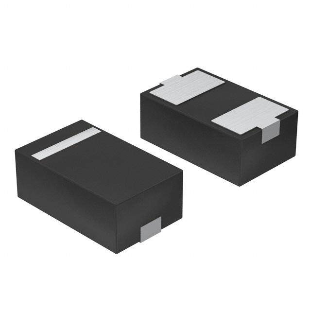
| 供应商器件封装 | DO-214AA (SMBJ) |
| 其它名称 | SMBJ3V3-E3/52GICT |
| 击穿电压 | 4.1 V |
| 功率-峰值脉冲 | 600W |
| 包装 | 剪切带 (CT) |
| 单向通道 | 1 |
| 双向通道 | - |
| 商标 | Vishay Semiconductors |
| 商标名 | TransZorb |
| 安装类型 | 表面贴装 |
| 安装风格 | SMD/SMT |
| 封装 | Reel |
| 封装/外壳 | DO-214AA,SMB |
| 封装/箱体 | DO-214AA |
| 尺寸 | 3.94 mm W x 4.57 mm L x 2.44 mm H |
| 峰值浪涌电流 | 200 A |
| 峰值脉冲功率耗散 | 600 W |
| 工作温度 | -65°C ~ 175°C (TJ) |
| 工厂包装数量 | 750 |
| 应用 | 通用 |
| 最大工作温度 | + 150 C |
| 最小工作温度 | - 55 C |
| 极性 | Unidirectional |
| 标准包装 | 1 |
| 电压-击穿(最小值) | 4.1V |
| 电压-反向关态(典型值) | 3.3V |
| 电压-箝位(最大值)@Ipp | 10.3V |
| 电流-峰值脉冲(10/1000µs) | 200A (8/20µs) |
| 电源线路保护 | 无 |
| 端接类型 | SMD/SMT |
| 类型 | 齐纳 |
| 系列 | SMBJ5.0A thru SMBJ188A |
| 钳位电压 | 10.3 V |


- 商务部:美国ITC正式对集成电路等产品启动337调查
- 曝三星4nm工艺存在良率问题 高通将骁龙8 Gen1或转产台积电
- 太阳诱电将投资9.5亿元在常州建新厂生产MLCC 预计2023年完工
- 英特尔发布欧洲新工厂建设计划 深化IDM 2.0 战略
- 台积电先进制程称霸业界 有大客户加持明年业绩稳了
- 达到5530亿美元!SIA预计今年全球半导体销售额将创下新高
- 英特尔拟将自动驾驶子公司Mobileye上市 估值或超500亿美元
- 三星加码芯片和SET,合并消费电子和移动部门,撤换高东真等 CEO
- 三星电子宣布重大人事变动 还合并消费电子和移动部门
- 海关总署:前11个月进口集成电路产品价值2.52万亿元 增长14.8%


PDF Datasheet 数据手册内容提取
SMBJ3V3 www.vishay.com Vishay General Semiconductor Surface Mount TRANSZORB® Transient Voltage Suppressors FEATURES • Uni-directional polarity only • Peak pulse power: 600 W (10/1000 μs) • Excellent clamping capability • Very fast response time • Meets MSL level 1, per J-STD-020, LF maximum peak of 260 °C • AEC-Q101 qualified • Material categorization: for definitions of compliance please see www.vishay.com/doc?99912 TYPICAL APPLICATIONS SMB (DO-214AA) Use in sensitive electronics protection against voltage transients induced by inductive load switching and lighting on ICs, MOSFET, signal lines of sensor units specifically for protecting 3.3 V supplied sensitive equipment against PRIMARY CHARACTERISTICS transient overvoltages. V (uni-directional) 4.1 V BR MECHANICAL DATA V 3.3 V WM Case: SMB (DO-214AA) P 600 W PPM Molding compound meets UL 94 V-0 flammability rating P 5 W D Base P/N-E3 - RoHS-compliant and commercial grade IFSM (uni-directional only) 60 A Base P/NHE3 - RoHS-compliant and AEC-Q101 qualified T max. 175 °C J Terminals: matte tin plated leads, solderable per Polarity Uni-directional J-STD-002 and JESD 22-B102 Package SMB (DO-214AA) E3 suffix meets JESD 201 class 2 whisker test, HE3 suffix meets JESD 201 class 2 whisker test Polarity: color band denotes cathode end MAXIMUM RATINGS (T = 25 °C unless otherwise noted) A PARAMETER SYMBOL VALUE UNIT Peak pulse power dissipation (1)(2) P 600 W PPM Peak pulse current with a 10/1000 μs waveform (fig. 1) I 50 A PP Peak pulse current with a 8/20 μs waveform (fig. 1) I 200 A PPM Peak forward surge current 8.3 ms single half sine-wave (2) I 60 A FSM Power dissipation on infinite heatsink, T = 75 °C P 5 W A D Operating junction and storage temperature range T , T -65 to +175 °C J STG Notes (1) Non-repetitive current pulse, per fig. 1 (2) Mounted on 0.2" x 0.2" (5.0 mm x 5.0 mm) copper pads to each terminal ELECTRICAL CHARACTERISTICS (T = 25 °C unless otherwise noted) A BREAKDOWN MAXIMUM MAXIMUM MAXIMUM TYPICAL TYPICAL VOLTAGE REVERSE STAND-OFF CLAMPING CLAMPING JUNCTION DTYEPVEICE MDACEROVKDICIENEG MINVB.R AT IT CLIEU AARTKR AVEGNET VOVLWTAMGE 1VV0OC/1 LA0TT0A0 IG PμPEs VVC8O /AL2TT0 A IμPGsPEM TCEOMEOPFEFFR VICABITRE UNRTE CACPA1J CAMTITH 0Az NVCE R WM V mA μA V V A V A 10-4/°C pF SMBJ3V3 KC 4.1 1.0 200 3.3 7.3 50 10.3 200 -5.3 5200 Revision: 16-Jan-18 1 Document Number: 88940 For technical questions within your region: DiodesAmericas@vishay.com, DiodesAsia@vishay.com, DiodesEurope@vishay.com THIS DOCUMENT IS SUBJECT TO CHANGE WITHOUT NOTICE. THE PRODUCTS DESCRIBED HEREIN AND THIS DOCUMENT ARE SUBJECT TO SPECIFIC DISCLAIMERS, SET FORTH AT www.vishay.com/doc?91000
SMBJ3V3 www.vishay.com Vishay General Semiconductor THERMAL CHARACTERISTICS (T = 25 °C unless otherwise noted) A PARAMETER SYMBOL VALUE UNIT Typical thermal resistance, junction to lead (1) R 20 JL °C/ W Typical thermal resistance, junction to ambient (2) R 100 JA Notes (1) Thermal resistance from junction to lead - mounted on 0.2" x 0.2" (5.0 mm x 5.0 mm) copper pads to each terminal (2) Thermal resistance from junction to ambient - mounted on the recommended PCB pad layout ORDERING INFORMATION (Example) PREFERRED P/N UNIT WEIGHT (g) PREFERRED PACKAGE CODE BASE QUANTITY DELIVERY MODE SMBJ3V3-E3/52 0.096 52 750 7" diameter plastic tape and reel SMBJ3V3-E3/5B 0.096 5B 3200 13" diameter plastic tape and reel SMBJ3V3HE3/52 (1) 0.096 52 750 7" diameter plastic tape and reel SMBJ3V3HE3/5B (1) 0.096 5B 3200 13" diameter plastic tape and reel Note (1) AEC-Q101 qualified RATINGS AND CHARACTERISTICS CURVES (T = 25 °C unless otherwise noted) A 150 10 t = 10 µs TJ = 25 °C RSM trr = 8 µs iPsu dlseefi nWeidd tahs ( tthd)e Point ulse Current, % I 100 PIPePaMk ValueHIPaPMlf Valuwdee h-cearIyeP2s Pt htoe 5P0e a%k oCfu IrPrPeMnt (T = 25 °C) RJ 1 - Peak PM 50 ttdd == 12000 µ0s µs I (T)/IRJ P P I t d 0 0.1 0 1.0 2.0 3.0 4.0 0 25 50 75 100 125 150 175 t - Time (ms) TJ - Junction Temperature (°C) Fig. 1 - Pulse Wave Form Fig. 3 - Relative Variation of Leakage Current vs. Junction Temperature 10 10 W) k wer ( e (V) 8 Po ag Pulse 1 g Volt ak pin Pe m 6 - PM Cla 10/1000 µs P P 8/20 µs 0.1 4 0.01 0.1 1 10 0.1 1 10 100 1000 t - Pulse Width (ms) I (A) d PP Fig. 2 - Peak Pulse Power Rating Curve Fig. 4 - Clamping Voltage vs. Peak Pulse Current (TJ initial = 25 °C) Revision: 16-Jan-18 2 Document Number: 88940 For technical questions within your region: DiodesAmericas@vishay.com, DiodesAsia@vishay.com, DiodesEurope@vishay.com THIS DOCUMENT IS SUBJECT TO CHANGE WITHOUT NOTICE. THE PRODUCTS DESCRIBED HEREIN AND THIS DOCUMENT ARE SUBJECT TO SPECIFIC DISCLAIMERS, SET FORTH AT www.vishay.com/doc?91000
SMBJ3V3 www.vishay.com Vishay General Semiconductor 5500 100 )Fp5000 A) ( ecnatic4500 Current ( 10 TJ = 175 °C TJ = 25 °C apa4000 ard C w noitc3500 k For 1 nu3000 ea J P - CJ2500 I - F 2000 0.1 0 0.5 1 1.5 2 2.5 3 3.5 0 0.2 0.4 0.6 0.8 1 1.2 1.4 1.6 1.8 Reverse Voltage (V) V - Forward Voltage Drop (V) F Fig. 5 - Typical Junction Capacitance Fig. 7 - Typical Peak Forward Voltage Drop vs. Peak Forward Current 100 )W /C °( e c n a d e p m I la 10 m re h T tn e is n a rT 1 0.01 0.1 1 10 100 1000 t - Pulse Duration (s) Fig. 6 - Typical Transient Thermal Impedance PACKAGE OUTLINE DIMENSIONS in inches (millimeters) SMB (DO-214AA) Mounting Pad Layout Cathode Band 0.085 (2.159) MAX. 0.086 (2.20) 0.155 (3.94) 0.077 (1.95) 0.130 (3.30) 0.086 (2.18) MIN. 0.180 (4.57) 0.160 (4.06) 0.060 (1.52) 0.012 (0.305) MIN. 0.006 (0.152) 0.096 (2.44) 0.220 REF. 0.084 (2.13) 0.060 (1.52) 0.030 (0.76) 0.008 (0.2) 0 (0) 0.220 (5.59) 0.205 (5.21) Revision: 16-Jan-18 3 Document Number: 88940 For technical questions within your region: DiodesAmericas@vishay.com, DiodesAsia@vishay.com, DiodesEurope@vishay.com THIS DOCUMENT IS SUBJECT TO CHANGE WITHOUT NOTICE. THE PRODUCTS DESCRIBED HEREIN AND THIS DOCUMENT ARE SUBJECT TO SPECIFIC DISCLAIMERS, SET FORTH AT www.vishay.com/doc?91000
Legal Disclaimer Notice www.vishay.com Vishay Disclaimer ALL PRODUCT, PRODUCT SPECIFICATIONS AND DATA ARE SUBJECT TO CHANGE WITHOUT NOTICE TO IMPROVE RELIABILITY, FUNCTION OR DESIGN OR OTHERWISE. Vishay Intertechnology, Inc., its affiliates, agents, and employees, and all persons acting on its or their behalf (collectively, “Vishay”), disclaim any and all liability for any errors, inaccuracies or incompleteness contained in any datasheet or in any other disclosure relating to any product. Vishay makes no warranty, representation or guarantee regarding the suitability of the products for any particular purpose or the continuing production of any product. To the maximum extent permitted by applicable law, Vishay disclaims (i) any and all liability arising out of the application or use of any product, (ii) any and all liability, including without limitation special, consequential or incidental damages, and (iii) any and all implied warranties, including warranties of fitness for particular purpose, non-infringement and merchantability. Statements regarding the suitability of products for certain types of applications are based on Vishay’s knowledge of typical requirements that are often placed on Vishay products in generic applications. Such statements are not binding statements about the suitability of products for a particular application. It is the customer’s responsibility to validate that a particular product with the properties described in the product specification is suitable for use in a particular application. Parameters provided in datasheets and / or specifications may vary in different applications and performance may vary over time. All operating parameters, including typical parameters, must be validated for each customer application by the customer’s technical experts. Product specifications do not expand or otherwise modify Vishay’s terms and conditions of purchase, including but not limited to the warranty expressed therein. Except as expressly indicated in writing, Vishay products are not designed for use in medical, life-saving, or life-sustaining applications or for any other application in which the failure of the Vishay product could result in personal injury or death. Customers using or selling Vishay products not expressly indicated for use in such applications do so at their own risk. Please contact authorized Vishay personnel to obtain written terms and conditions regarding products designed for such applications. No license, express or implied, by estoppel or otherwise, to any intellectual property rights is granted by this document or by any conduct of Vishay. Product names and markings noted herein may be trademarks of their respective owners. © 2017 VISHAY INTERTECHNOLOGY, INC. ALL RIGHTS RESERVED Revision: 08-Feb-17 1 Document Number: 91000
Mouser Electronics Authorized Distributor Click to View Pricing, Inventory, Delivery & Lifecycle Information: V ishay: SMBJ3V3/52 SMBJ3V3/55 SMBJ3V3/5B SMBJ3V3-E3/52 SMBJ3V3-E3/55 SMBJ3V3-E3/5B SMBJ3V3HE3/52 SMBJ3V3HE3/5B