ICGOO在线商城 > 集成电路(IC) > PMIC - 电源管理 - 专用 > SM72295MAE/NOPB

 Datasheet下载
- 型号: SM72295MAE/NOPB
- 制造商: Texas Instruments
- 库位|库存: xxxx|xxxx
- 要求:
| 数量阶梯 | 香港交货 | 国内含税 |
| +xxxx | $xxxx | ¥xxxx |
查看当月历史价格
查看今年历史价格
SM72295MAE/NOPB产品简介:
ICGOO电子元器件商城为您提供SM72295MAE/NOPB由Texas Instruments设计生产,在icgoo商城现货销售,并且可以通过原厂、代理商等渠道进行代购。 SM72295MAE/NOPB价格参考。Texas InstrumentsSM72295MAE/NOPB封装/规格:PMIC - 电源管理 - 专用, Photovoltaics PMIC 28-SOIC。您可以下载SM72295MAE/NOPB参考资料、Datasheet数据手册功能说明书,资料中有SM72295MAE/NOPB 详细功能的应用电路图电压和使用方法及教程。
Texas Instruments的SM72295MAE/NOPB是一款专为电源管理设计的PMIC(电源管理集成电路),特别适用于需要高效、紧凑和可靠电源解决方案的应用场景。这款芯片集成了多种电源管理功能,能够为系统提供稳定的电压和电流输出,确保设备在各种工作条件下的稳定运行。

 应用场景:

1. 便携式电子设备:
   SM72295MAE/NOPB非常适合用于便携式电子设备,如智能手机、平板电脑、智能手表等。这些设备通常对功耗和体积有严格要求,而该芯片的高集成度和低功耗特性可以有效延长电池寿命,同时减少电路板空间占用。

2. 工业控制系统:
   在工业自动化和控制系统中,电源管理至关重要。SM72295MAE/NOPB可以为PLC(可编程逻辑控制器)、传感器、执行器等提供稳定的电源供应,确保系统的可靠性和稳定性。其宽输入电压范围和多种保护机制使其能够在复杂的工业环境中稳定工作。

3. 通信设备:
   通信基础设施设备,如基站、路由器和交换机,需要高效的电源管理来支持其高性能处理器和网络接口。SM72295MAE/NOPB能够提供多路输出,满足不同模块的供电需求,同时具备快速响应和低噪声特性,确保通信质量。

4. 医疗设备:
   医疗设备对电源的安全性和可靠性要求极高。SM72295MAE/NOPB的多重保护功能(如过流保护、过温保护等)以及其高精度的电压调节能力,使其成为便携式医疗设备(如血糖仪、心率监测器)的理想选择。

5. 汽车电子:
   汽车电子系统中,电源管理芯片需要应对复杂的电气环境和严格的性能要求。SM72295MAE/NOPB可以为车载信息娱乐系统、ADAS(高级驾驶辅助系统)等提供稳定的电源支持,确保车辆电子系统的正常运行。

总之,SM72295MAE/NOPB凭借其高效、紧凑和可靠的电源管理特性,广泛应用于各类对电源要求较高的领域,为现代电子产品提供了强大的电源保障。
| 参数 | 数值 |
| 产品目录 | 集成电路 (IC)半导体 |
| 描述 | IC PHOTO FULL BRIDGE DR 28SOIC门驱动器 Photovoltaic Full Bridge Driver 28-SOIC -40 to 125 |
| 产品分类 | |
| 品牌 | Texas Instruments |
| 产品手册 | |
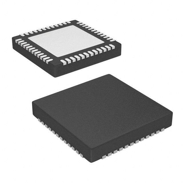
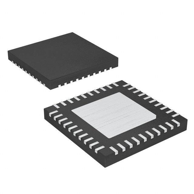
| 产品图片 |
|
| rohs | 符合RoHS无铅 / 符合限制有害物质指令(RoHS)规范要求 |
| 产品系列 | 电源管理 IC,门驱动器,Texas Instruments SM72295MAE/NOPBSolarMagic™ |
| 数据手册 | |
| 产品型号 | SM72295MAE/NOPB |
| 上升时间 | 8 ns |
| 下降时间 | 8 ns |
| 产品 | MOSFET Gate Drivers |
| 产品种类 | 门驱动器 |
| 供应商器件封装 | 28-SOIC |
| 其它名称 | SM72295MAE/NOPBDKR |
| 包装 | Digi-Reel® |
| 参考设计库 | http://www.digikey.com/rdl/4294959902/4294959891/133 |
| 商标 | Texas Instruments |
| 安装类型 | 表面贴装 |
| 安装风格 | SMD/SMT |
| 封装 | Reel |
| 封装/外壳 | 28-SOIC(0.295",7.50mm 宽) |
| 封装/箱体 | SOIC-28 |
| 工作温度 | -40°C ~ 125°C |
| 工厂包装数量 | 250 |
| 应用 | 光电型 |
| 最大关闭延迟时间 | 26 ns |
| 最大工作温度 | + 125 C |
| 最大开启延迟时间 | 26 ns |
| 最小工作温度 | - 40 C |
| 标准包装 | 1 |
| 特色产品 | http://www.digikey.com/product-highlights/cn/zh/texas-instruments-solar-micro-inverter/1289 |
| 电压-电源 | 3 V ~ 7 V, 8 V ~ 14 V |
| 电流-电源 | 25µA |
| 电源电压-最大 | 14 V |
| 电源电压-最小 | 8 V |
| 电源电流 | 2.2 mA |
| 类型 | Dual Full-Bridge Driver |
| 系列 | SM72295 |
| 输出电流 | 3 A |
| 配置 | Dual |


PDF Datasheet 数据手册内容提取
SM72295 www.ti.com SNVS688E–OCTOBER2010–REVISEDAPRIL2013 SM72295 Photovoltaic Full Bridge Driver CheckforSamples:SM72295 FEATURES DESCRIPTION 1 • RenewableEnergyGrade The SM72295 is designed to drive 4 discrete N type 2 MOSFET’s in a full bridge configuration. The drivers • DualHalfBridgeMOSFETDrivers provide 3A of peak current for fast efficient switching • Integrated100VBootstrapDiodes and integrated high speed bootstrap diodes. Current • IndependentHighandLowDriverLogicInputs sensing is provided by 2 transconductance amplifiers with externally programmable gain and filtering to • BootstrapSupplyVoltageRangeupto115V remove ripple current to provide average current DC information to the control circuit. The current sense • TwoCurrentSenseAmplifierswithExternally amplifiers have buffered outputs available to provide ProgrammableGainandBufferedOutputs a low impedance interface to an A/D converter if needed. An externally programmable input over • ProgrammableOverVoltageProtection voltage comparator is also included to shutdown all • SupplyRailUnder-VoltageLockoutswith outputs. Under voltage lockout with a PGOOD PowerGoodIndicator indicator prevents the drivers from operating if VCC is toolow. PACKAGE • SOIC-28 Typical Application Circuit + 1R01m6 1R01m5 + R10 R11 R12 Vout PV Vin R9 C1 R13R14 10k - - C5 C4 0.47 uF C6 C3 0.47 uF 5V 1 1 uF uF 10V HSA HOA HBA VCCA LOA PGND LOB VCCB HBB HOB HSB VDD OVS OVP 5 9 2 2 7 M S R6 SIA SOA IIN BIN AGND LIA HIA HIB LIB PGOOD BOUT IOUT SOB SIB R7 500 500 C10 C8 R8 10n 10 nF 500 R5 optional optional 500 C7 4R03k C2 R4 40k 1 Pleasebeawarethatanimportantnoticeconcerningavailability,standardwarranty,anduseincriticalapplicationsof TexasInstrumentssemiconductorproductsanddisclaimerstheretoappearsattheendofthisdatasheet. Alltrademarksarethepropertyoftheirrespectiveowners. 2 PRODUCTIONDATAinformationiscurrentasofpublicationdate. Copyright©2010–2013,TexasInstrumentsIncorporated Products conform to specifications per the terms of the Texas Instruments standard warranty. Production processing does not necessarilyincludetestingofallparameters.
SM72295 SNVS688E–OCTOBER2010–REVISEDAPRIL2013 www.ti.com Connection Diagram 1 28 SIA HSA 2 27 SOA HOA 3 26 IIN HBA 4 BIN VCCA 25 5 AGND LOA 24 6 LIA PGND 23 7 22 HIA LOB SM72295 8 21 HIB VCCB 9 LIB HBB 20 10 PGOOD HOB 19 11 18 BOUT HSB 12 17 IOUT VDD 13 16 SOB OVS 14 SIB OVP 15 Figure1. TopView SOIC-28 PINDESCRIPTIONS Pin Name Description ApplicationInformation 1 SIA Sensehighinputforinputcurrent Tietopositivesideofthecurrentsenseresistorthroughanexternalgain sensetransconductanceamplifier programmingresistor(RI).Amplifiertransconductanceis1/RI. 2 S0A Senselowinputforinputcurrent Tietonegativesideofthecurrentsenseresistorthroughanexternalgain sensetransconductanceamplifier programmingresistor.Amplifiertransconductanceis1/RI. 3 IIN Outputforcurrentsense Outputoftheinputcurrentsenseamplifier.Requiresanexternalresistorto transconductanceamplifier ground(RL).GainisRL/RI,whereRIistheexternalresistorinserieswiththe SIApin. 4 BIN BufferedIIN BufferedIIN. 5 AGND Analogground Groundreturnfortheanalogcircuitry.TietothegroundplaneundertheIC 6,9 LIA,LIB Lowsidedrivercontrolinput TheinputshaveTTLtypethresholds.Unusedinputsshouldbetiedtoground andnotleftopen. 7,8 HIA,HIB Highsidedrivercontrolinput TheinputshaveTTLtypethresholds.Unusedinputsshouldbetiedtoground andnotleftopen. 10 PGOOD Powergoodindicatoroutput Opendrainoutputwithaninternalpull-upresistortoVDDindicatingVCCisin regulation.PGOODlowimpliesVCCisoutofregulation. 11 BOUT BufferedIOUT BufferedIOUT. 12 IOUT Outputforcurrentsense Outputoftheoutputcurrentsenseamplifier.Requiresanexternalresistorto comparator. ground(RL).GainisRL/RI,whereRIistheexternalresistorinserieswiththe SIBpin. 13 S0B Senselowinputforoutputcurrent Tietonegativesideofthecurrentsenseresistorthroughanexternalgain senseamplifier programmingresistor.Amplifiertransconductanceis1/RI. 14 SIB Sensehighinputforoutputcurrent Tietopositivesideofthecurrentsenseresistorthroughanexternalgain senseamplifier programmingresistor(RI).Amplifiertransconductanceis1/RI. 15 OVP Overvoltageindicatoroutput Opendrainoutputwithaninternalpull-upresistortoVDDindicatingOVS>VDD. OVPislowwhenOVS>VDD. 16 OVS Senseinputforovervoltage Requiresanexternalresistordivider.VDDisthereferencevoltage. 17 VDD 3.3Vor5Vregulatoroutput Bypasswith0.1uF.ReferenceforovervoltageshutdownandIOUT/IINclamp 18,28 HSA, HighsideMOSFETsource Connecttobootstrapcapacitornegativeterminalandthesourceofthehighside HSB connection MOSFET. 2 SubmitDocumentationFeedback Copyright©2010–2013,TexasInstrumentsIncorporated ProductFolderLinks:SM72295
SM72295 www.ti.com SNVS688E–OCTOBER2010–REVISEDAPRIL2013 PINDESCRIPTIONS(continued) Pin Name Description ApplicationInformation 19,27 HOA, Highsidegatedriveroutput ConnecttogateofhighsideMOSFETwithashortlowinductancepath. HOB 20,26 HBA, Highsidegatedriverbootstraprail. ConnectthepositiveterminalofthebootstrapcapacitortoHBandthenegative HBB terminaltoHS.ThebootstrapcapacitorshouldbeplacedasclosetoICas possible. 21,25 VCCA, Positivegatedrivesupply LocallydecoupletoPGNDusinglowESR/ESLcapacitorlocatedasclosetoIC VCCB aspossible. 22,24 LOA, Lowsidegatedriveroutput ConnecttothegateofthelowsideMOSFETwithashortlowinductancepath. LOB 23 PGND Powergroundreturn GroundreturnfortheLOdrivers.TietothegroundplaneundertheIC Thesedeviceshavelimitedbuilt-inESDprotection.Theleadsshouldbeshortedtogetherorthedeviceplacedinconductivefoam duringstorageorhandlingtopreventelectrostaticdamagetotheMOSgates. Absolute Maximum Ratings(1)(2) VCCA,VCCB -0.3to14V VDD -0.3to7V HBAtoHSA,HBBtoHSB -0.3to15V LIA,LIB,HIA,HIB,OVS -0.3to7V LOA,LOB -0.3toVCC+0.3V HOA,HOB HS–0.3toHB+0.3V SIA,SOA,SIB,SOB -0.3to100V SIAtoSOA,SIBtoSOB -0.8to0.8V HSA,HSB(3) -5to100V HBA,HBB 115V PGOOD,OVP -0.3toVDD IIN,IOUT -0.3toVDD BIN,BOUT -0.3toVDD JunctionTemperature 150°C StorageTemperatueRange -55°Cto+150°C ESDRating(4) HumanBodyModel 2kV (1) AbsoluteMaximumRatingsindicatelimitsbeyondwhichdamagetothecomponentmayoccur.OperatingRatingsareconditionsunder whichoperationofthedeviceisensured.OperatingRatingsdonotimplyensuredperformancelimits.Forensuredperformancelimits andassociatedtestconditions,seetheElectricalCharacteristicstables. (2) IfMilitary/Aerospacespecifieddevicesarerequired,pleasecontacttheTISalesOffice/Distributorsforavailabilityandspecifications. (3) IntheapplicationtheHSnodesareclampedbythebodydiodeoftheexternallowerN-MOSFET,thereforetheHSnodewillgenerally notexceed–1V.However,insomeapplications,boardresistanceandinductancemayresultintheHSnodeexceedingthisstated voltagetransiently.Ifnegativetransientsoccur,theHSvoltagemustneverbemorenegativethanVCC-15V.ForexampleifVCC=10V, thenegativetransientsatHSmustnotexceed–5V. (4) Thehumanbodymodelisa100pFcapacitordischargedthrougha1.5kΩresistorintoeachpin.2kVforallpinsexceptHB,HO&HS whichareratedat1000V. Copyright©2010–2013,TexasInstrumentsIncorporated SubmitDocumentationFeedback 3 ProductFolderLinks:SM72295
SM72295 SNVS688E–OCTOBER2010–REVISEDAPRIL2013 www.ti.com Recommended Operating Conditions VCCA,VCCB +8Vto+14V VDD +3Vto7V SI,SOcommonmode VDD+1Vto100V HS(1) -1Vto100V HBA,HBB HS+7VtoHS+14V HSSlewRate <50V/ns JunctionTemperature -40°Cto+125°C (1) IntheapplicationtheHSnodesareclampedbythebodydiodeoftheexternallowerN-MOSFET,thereforetheHSnodewillgenerally notexceed–1V.However,insomeapplications,boardresistanceandinductancemayresultintheHSnodeexceedingthisstated voltagetransiently.Ifnegativetransientsoccur,theHSvoltagemustneverbemorenegativethanVCC-15V.ForexampleifVCC=10V, thenegativetransientsatHSmustnotexceed–5V. Electrical Characteristics(1) SpecificationsinstandardtypefaceareforT =25°C,andthoseinboldfacetypeapplyoverthefulloperatingjunction J temperaturerange.NoloadonLO&HO,VCC=10V,VDD=5V,HB-HS=10V,OVS=0Vunlessotherwiseindicated. Symbol Parameter Conditions Min Typ Max Units SUPPLYCURRENTS I VDDQuiescentCurrent SIA=SOB,SIB=SOB. 25 40 μA DD VCCQuiescentCurrent I Alloutputsoff 500 800 μA CC (ICCA+ICCB) VCCOperatingCurrent I LOA&LOBswitchingat200kHz 2.2 3 mA CCO (ICCA+ICCB) I HBA,HBBQuiescentCurrent Alloutputsoff 55 200 μA HB I HBA,HBBOperatingCurrent HOA&HOBswitchingat200kHz 700 1000 μA HBO HBA&HBBtoV Current, I SS HS=100V,HB=110V 0.1 10 μA HBS Quiescent HBAandHBBtoV Current, I SS f=200kHz 130 μA HBSO Operating PGOOD,OVBOUTPUTs V OutputLowRDS 25 50 Ω OL R VDDpullupresistor 50 90 kΩ PU LI,HIINPUTPINS V InputVoltageThreshold 1.3 1.8 2.3 V IL V InputVoltageHysteresis 50 mV IHYS R LI,HIPulldownResistance 100 200 400 kΩ I OVERVOLTAGESHUTDOWN V OVSRisingThreshold VDD-50mV VDD VDD+50mV V OVR V OVSthresholdHysteresis 5% VDD OVH I OVSinputbiascurrent OVS<VDD 1 nA OVS UNDERVOLTAGESHUTDOWN V VCCRisingThreshold 6 6.9 7.4 V CCR V VCCthresholdHysteresis 0.5 V CCH V HB-HSRisingThreshold 5.7 6.6 7.1 V HBR V HB-HSThresholdHysteresis 0.4 V HBH BOOTSTRAPDIODE V High-CurrentForwardVoltage I =100mA 0.8 1 V DH VCC-HB R DynamicResistance I =100mA 1 1.65 Ω D VCC-HB (1) MinandMaxlimitsare100%productiontestedat25ºC.Limitsovertheoperatingtemperaturerangeareensuredthroughcorrelation usingStatisticalQualityControl(SQC)methods.LimitsareusedtocalculateAverageOutgoingQualityLevel(AOQL). 4 SubmitDocumentationFeedback Copyright©2010–2013,TexasInstrumentsIncorporated ProductFolderLinks:SM72295
SM72295 www.ti.com SNVS688E–OCTOBER2010–REVISEDAPRIL2013 Electrical Characteristics(1) (continued) SpecificationsinstandardtypefaceareforT =25°C,andthoseinboldfacetypeapplyoverthefulloperatingjunction J temperaturerange.NoloadonLO&HO,VCC=10V,VDD=5V,HB-HS=10V,OVS=0Vunlessotherwiseindicated. Symbol Parameter Conditions Min Typ Max Units LO&HOGATEDRIVER I =100mA V Low-LevelOutputVoltage LO 0.16 0.4 V OL V =LO-PGNDorHO-HS OL I =-100mA V High-LevelOutputVoltage LO 0.28 0.6 V OH V =VCC-LOorVCC-HO OH I PeakPullupCurrent HO,LO=12V 3 A OHL I PeakPulldownCurrent HO,LO=0V 3 A OLL t LOTurn-OffPropagationDelay LIFallingtoLOFalling 22 ns LPHL t LOTurn-OnPropagationDelay LIRisingtoLORising 26 ns LPLH t HOTurn-OffPropagationDelay HIFallingtoHOFalling 22 ns HPHL t LOTurn-OnPropagationDelay HIRisingtoHORising 26 ns HPLH DelayMatching:LOon&HO t 1 ns MON off DelayMatching:LOoff&HO t 1 ns MOFF on t ,t EitherOutputRise/FallTime C =1000pF 8 ns RC FC L MinimumInputPulseWidththat t 50 ns PW ChangestheOutput BootstrapDiodeTurn-Onor t I =100mA/I =100mA 37 ns BS Turn-OffTime F R CURRENTSENSEAMPLIFIER R =R =500,10mVsense V Offsetvoltage SI SO -2 2 mV OS resistorvoltage Gainisprogrammedwith 5mVsenseresistorvoltage Gain5mV externalresistors 390 mV R =R =1000,R =75K IOUT,IIN=(RL/RSI)*(SI-SO) SI SO L Gainisprogrammedwith Gain 50mVsenseresistorvoltage externalresistors 3.85 V 50mV R =R =1000,R =75K IOUT,IIN=(RL/RSI)*(SI-SO) SI SO L 0.1Vsenseresistorvoltage Vclamp OutputClamp VDD V R =R =1000,R =75K SI SO L CURRENTSENSEBUFFER Offsetvoltage(BIN-IIN), IIN=2.5V -60 60 mV (BOUT-IOUT) OutputlowvoltageBOUT,BIN IIN,IOUT=0 0 50 mV OutputhighvoltageBOUT,BIN IIN,IOUT=VDD VDD-100mV VDD-30mV VDD mV THERMALRESISTANCE θ JunctiontoAmbient SOIC-28(2) 60 °C/W JA (2) 2layerboardwith2ozCuusingJEDECJESD51thermalboard. Copyright©2010–2013,TexasInstrumentsIncorporated SubmitDocumentationFeedback 5 ProductFolderLinks:SM72295
SM72295 SNVS688E–OCTOBER2010–REVISEDAPRIL2013 www.ti.com Block Diagram A B A B HBB LI LI HI HI VCCB VDD UVLO 3V HOB 3V LEVEL DRIVER 200k SHIFT HSB HBA VCCA UVLO HOA VDD LEVEL DRIVER VCC SHIFT 50k UVLO 3V HSA PGOOD VCCA 3V VDD LOB DRIVER 50k PGND OVP VCCB 3V OVS LOA + DRIVER VDD 3.3V/5V PGND - SIA SIB SOA SOB + + _ _ IIN IOUT + + _ _ VDD VDD CLAMP CLAMP BOUT BIN AGND Figure2. BlockDiagram 6 SubmitDocumentationFeedback Copyright©2010–2013,TexasInstrumentsIncorporated ProductFolderLinks:SM72295
SM72295 www.ti.com SNVS688E–OCTOBER2010–REVISEDAPRIL2013 Typical Performance Characteristics OperatingCurrent VCCUndervoltageRisingThreshold vsTemperature vsTemperature Figure3. Figure4. VCCQuiescentCurrent VCCUndervoltageThresholdHysteresis vsTemperature vsTemperature Figure5. Figure6. VDDQuiescentCurrent GateDriveHighLevelOutputVoltage vsTemperature vsTemperature Figure7. Figure8. Copyright©2010–2013,TexasInstrumentsIncorporated SubmitDocumentationFeedback 7 ProductFolderLinks:SM72295
SM72295 SNVS688E–OCTOBER2010–REVISEDAPRIL2013 www.ti.com Typical Performance Characteristics (continued) GateDriveLowlevelOutputVoltage BootstrapDiodeForwardVoltage vsTemperature vsTemperature Figure9. Figure10. CurrentSenseAmplifierInputOffsetVoltage CurrentSenseAmplifierOutputBufferOffsetVoltage vsTemperature vsTemperature Figure11. Figure12. 8 SubmitDocumentationFeedback Copyright©2010–2013,TexasInstrumentsIncorporated ProductFolderLinks:SM72295
SM72295 www.ti.com SNVS688E–OCTOBER2010–REVISEDAPRIL2013 Timing Diagram LI LI HI HI tHPLH tLPLH tHPHL tLPHL LO LO HO HO tMON tMOFF Power Dissipation Considerations The total IC power dissipation is the sum of the gate driver losses and the bootstrap diode losses. The gate driver losses are related to the switching frequency (f), output load capacitance on LO and HO (C ), and supply L voltage(V )andcanberoughlycalculatedas: DD P =2•f•C •V 2 (1) DGATES L DD There are some additional losses in the gate drivers due to the internal CMOS stages used to buffer the LO and HO outputs. The following plot shows the measured gate driver power dissipation versus frequency and load capacitance. At higher frequencies and load capacitance values, the power dissipation is dominated by the power losses driving the output loads and agrees well with the above equation. This plot can be used to approximatethepowerlossesduetothegatedrivers. Figure13. GateDriverPowerDissipation(LO+HO) V =12V,NeglectingDiodeLosses CC 1.000 CL = 4400 pF 0.100 R (W) CL = 1000 pF WE O P 0.010 CL = 0 pF 0.001 0.1 1.0 10.0 100.0 1000.0 SWITCHING FREQUENCY (kHz) The bootstrap diode power loss is the sum of the forward bias power loss that occurs while charging the bootstrap capacitor and the reverse bias power loss that occurs during reverse recovery. Since each of these events happens once per cycle, the diode power loss is proportional to frequency. Larger capacitive loads require more current to recharge the bootstrap capacitor resulting in more losses. Higher input voltages (V ) to IN the half bridge result in higher reverse recovery losses. The following plot was generated based on calculations and lab measurements of the diode recovery time and current under several operating conditions. This can be useful for approximating the diode power dissipation. The total IC power dissipation can be estimated from the previousplotsbysummingthegatedrivelosseswiththebootstrapdiodelossesfortheintendedapplication. Copyright©2010–2013,TexasInstrumentsIncorporated SubmitDocumentationFeedback 9 ProductFolderLinks:SM72295
SM72295 SNVS688E–OCTOBER2010–REVISEDAPRIL2013 www.ti.com Figure14. DiodePowerDissipationV =50V IN 0.100 CL = 4400 pF )W ( RE 0.010 CL = 0 pF W O P 0.001 1 10 100 1000 SWITCHING FREQUENCY (kHz) Layout Considerations The optimum performance of high and low-side gate drivers cannot be achieved without taking due considerationsduringcircuitboardlayout.Followingpointsareemphasized. 1. Low ESR / ESL capacitors must be connected close to the IC, between VDD and VSS pins and between the HB and HS pins to support the high peak currents being drawn from VDD during turn-on of the external MOSFET. 2. To prevent large voltage transients at the drain of the top MOSFET, a low ESR electrolytic capacitor must be connectedbetweenMOSFETdrainandground(VSS). 3. In order to avoid large negative transients on the switch node (HS pin), the parasitic inductances in the sourceoftopMOSFETandinthedrainofthebottomMOSFET(synchronousrectifier)mustbeminimized. 4. GroundingConsiderations: (a) The first priority in designing grounding connections is to confine the high peak currents that charge and discharge the MOSFET gate into a minimal physical area. This will decrease the loop inductance and minimizenoiseissuesonthegateterminaloftheMOSFET.TheMOSFETsshouldbeplacedascloseas possibletothegatedriver. (b) The second high current path includes the bootstrap capacitor, the bootstrap diode, the local ground referenced bypass capacitor and low-side MOSFET body diode. The bootstrap capacitor is recharged on a cycle-by-cycle basis through the bootstrap diode from the ground referenced VDD bypass capacitor. The recharging occurs in a short time interval and involves high peak current. Minimizing this loop length andareaonthecircuitboardisimportanttoensurereliableoperation. 10 SubmitDocumentationFeedback Copyright©2010–2013,TexasInstrumentsIncorporated ProductFolderLinks:SM72295
SM72295 www.ti.com SNVS688E–OCTOBER2010–REVISEDAPRIL2013 REVISION HISTORY ChangesfromRevisionD(April2013)toRevisionE Page • ChangedlayoutofNationalDataSheettoTIformat.......................................................................................................... 10 Copyright©2010–2013,TexasInstrumentsIncorporated SubmitDocumentationFeedback 11 ProductFolderLinks:SM72295
PACKAGE OPTION ADDENDUM www.ti.com 6-Feb-2020 PACKAGING INFORMATION Orderable Device Status Package Type Package Pins Package Eco Plan Lead/Ball Finish MSL Peak Temp Op Temp (°C) Device Marking Samples (1) Drawing Qty (2) (6) (3) (4/5) SM72295MA/NOPB ACTIVE SOIC DW 28 26 Green (RoHS NIPDAU Level-3-260C-168 HR -40 to 125 S72295 & no Sb/Br) SM72295MAX/NOPB ACTIVE SOIC DW 28 1000 Green (RoHS NIPDAU Level-3-260C-168 HR -40 to 125 S72295 & no Sb/Br) (1) The marketing status values are defined as follows: ACTIVE: Product device recommended for new designs. LIFEBUY: TI has announced that the device will be discontinued, and a lifetime-buy period is in effect. NRND: Not recommended for new designs. Device is in production to support existing customers, but TI does not recommend using this part in a new design. PREVIEW: Device has been announced but is not in production. Samples may or may not be available. OBSOLETE: TI has discontinued the production of the device. (2) RoHS: TI defines "RoHS" to mean semiconductor products that are compliant with the current EU RoHS requirements for all 10 RoHS substances, including the requirement that RoHS substance do not exceed 0.1% by weight in homogeneous materials. Where designed to be soldered at high temperatures, "RoHS" products are suitable for use in specified lead-free processes. TI may reference these types of products as "Pb-Free". RoHS Exempt: TI defines "RoHS Exempt" to mean products that contain lead but are compliant with EU RoHS pursuant to a specific EU RoHS exemption. Green: TI defines "Green" to mean the content of Chlorine (Cl) and Bromine (Br) based flame retardants meet JS709B low halogen requirements of <=1000ppm threshold. Antimony trioxide based flame retardants must also meet the <=1000ppm threshold requirement. (3) MSL, Peak Temp. - The Moisture Sensitivity Level rating according to the JEDEC industry standard classifications, and peak solder temperature. (4) There may be additional marking, which relates to the logo, the lot trace code information, or the environmental category on the device. (5) Multiple Device Markings will be inside parentheses. Only one Device Marking contained in parentheses and separated by a "~" will appear on a device. If a line is indented then it is a continuation of the previous line and the two combined represent the entire Device Marking for that device. (6) Lead/Ball Finish - Orderable Devices may have multiple material finish options. Finish options are separated by a vertical ruled line. Lead/Ball Finish values may wrap to two lines if the finish value exceeds the maximum column width. Important Information and Disclaimer:The information provided on this page represents TI's knowledge and belief as of the date that it is provided. TI bases its knowledge and belief on information provided by third parties, and makes no representation or warranty as to the accuracy of such information. Efforts are underway to better integrate information from third parties. TI has taken and continues to take reasonable steps to provide representative and accurate information but may not have conducted destructive testing or chemical analysis on incoming materials and chemicals. TI and TI suppliers consider certain information to be proprietary, and thus CAS numbers and other limited information may not be available for release. In no event shall TI's liability arising out of such information exceed the total purchase price of the TI part(s) at issue in this document sold by TI to Customer on an annual basis. Addendum-Page 1
PACKAGE OPTION ADDENDUM www.ti.com 6-Feb-2020 Addendum-Page 2
PACKAGE MATERIALS INFORMATION www.ti.com 17-Nov-2019 TAPE AND REEL INFORMATION *Alldimensionsarenominal Device Package Package Pins SPQ Reel Reel A0 B0 K0 P1 W Pin1 Type Drawing Diameter Width (mm) (mm) (mm) (mm) (mm) Quadrant (mm) W1(mm) SM72295MAX/NOPB SOIC DW 28 1000 330.0 24.4 10.8 18.4 3.2 12.0 24.0 Q1 PackMaterials-Page1
PACKAGE MATERIALS INFORMATION www.ti.com 17-Nov-2019 *Alldimensionsarenominal Device PackageType PackageDrawing Pins SPQ Length(mm) Width(mm) Height(mm) SM72295MAX/NOPB SOIC DW 28 1000 367.0 367.0 45.0 PackMaterials-Page2
None
IMPORTANTNOTICEANDDISCLAIMER TI PROVIDES TECHNICAL AND RELIABILITY DATA (INCLUDING DATASHEETS), DESIGN RESOURCES (INCLUDING REFERENCE DESIGNS), APPLICATION OR OTHER DESIGN ADVICE, WEB TOOLS, SAFETY INFORMATION, AND OTHER RESOURCES “AS IS” AND WITH ALL FAULTS, AND DISCLAIMS ALL WARRANTIES, EXPRESS AND IMPLIED, INCLUDING WITHOUT LIMITATION ANY IMPLIED WARRANTIES OF MERCHANTABILITY, FITNESS FOR A PARTICULAR PURPOSE OR NON-INFRINGEMENT OF THIRD PARTY INTELLECTUAL PROPERTY RIGHTS. These resources are intended for skilled developers designing with TI products. You are solely responsible for (1) selecting the appropriate TI products for your application, (2) designing, validating and testing your application, and (3) ensuring your application meets applicable standards, and any other safety, security, or other requirements. These resources are subject to change without notice. TI grants you permission to use these resources only for development of an application that uses the TI products described in the resource. Other reproduction and display of these resources is prohibited. No license is granted to any other TI intellectual property right or to any third party intellectual property right. TI disclaims responsibility for, and you will fully indemnify TI and its representatives against, any claims, damages, costs, losses, and liabilities arising out of your use of these resources. TI’s products are provided subject to TI’s Terms of Sale (www.ti.com/legal/termsofsale.html) or other applicable terms available either on ti.com or provided in conjunction with such TI products. TI’s provision of these resources does not expand or otherwise alter TI’s applicable warranties or warranty disclaimers for TI products. Mailing Address: Texas Instruments, Post Office Box 655303, Dallas, Texas 75265 Copyright © 2020, Texas Instruments Incorporated