ICGOO在线商城 > 晶体,振荡器,谐振器 > 振荡器 > SIT3807AI-D2-33EE-16.800000X
 Datasheet下载
- 型号: SIT3807AI-D2-33EE-16.800000X
- 制造商: SiTime
- 库位|库存: xxxx|xxxx
- 要求:
| 数量阶梯 | 香港交货 | 国内含税 |
| +xxxx | $xxxx | ¥xxxx |
查看当月历史价格
查看今年历史价格
SIT3807AI-D2-33EE-16.800000X产品简介:
ICGOO电子元器件商城为您提供SIT3807AI-D2-33EE-16.800000X由SiTime设计生产,在icgoo商城现货销售,并且可以通过原厂、代理商等渠道进行代购。 SIT3807AI-D2-33EE-16.800000X价格参考。SiTimeSIT3807AI-D2-33EE-16.800000X封装/规格:振荡器, 振荡器 16.8MHz LVCMOS,LVTTL VCXO 3.3V 启用/禁用 6-SMD,无引线。您可以下载SIT3807AI-D2-33EE-16.800000X参考资料、Datasheet数据手册功能说明书,资料中有SIT3807AI-D2-33EE-16.800000X 详细功能的应用电路图电压和使用方法及教程。
SiT3807AI-D2-33EE-16.800000X 是 SiTIME 公司生产的基于 MEMS(微机电系统)技术的振荡器,属于 SIT3807 系列。以下是该型号的应用场景:

 1. 通信设备
   - 无线通信模块:适用于 LTE、5G 小基站、Wi-Fi 模块等,提供高精度和稳定的时钟信号。
   - 网络交换机/路由器:为数据传输提供精确的时间基准,确保网络同步。

 2. 消费电子
   - 智能手表/可穿戴设备:其小型化设计和低功耗特性适合便携式设备。
   - 笔记本电脑/平板电脑:用于 USB、PCIe 和其他高速接口的时钟生成。

 3. 工业自动化
   - PLC(可编程逻辑控制器):为工业控制设备提供稳定时钟。
   - 传感器网络:支持实时数据采集和传输。

 4. 汽车电子
   - 信息娱乐系统:提供高可靠性的时钟信号,支持多媒体功能。
   - ADAS(高级驾驶辅助系统):满足对温度变化和振动环境下的稳定性要求。

 5. 医疗设备
   - 监护仪/超声设备:确保医疗设备在关键应用中的高性能和可靠性。

 特性优势:
- 高频率稳定性:±20ppm 的频率精度,适应各种复杂环境。
- 抗冲击和振动能力强:MEMS 技术使其在恶劣条件下仍能保持性能。
- 小型封装:2.5mm x 2.0mm 的尺寸适合空间受限的设计。
- 低功耗:适合电池供电设备,延长续航时间。

综上,SiT3807AI-D2-33EE-16.800000X 广泛应用于需要高精度、高可靠性和低功耗时钟信号的领域,尤其适合对环境适应性要求较高的场景。
| 参数 | 数值 |
| 产品目录 | 晶体和振荡器 |
| 描述 | OSC MEMS 16.80MHZ SMD |
| 产品分类 | |
| 品牌 | SiTIME |
| 数据手册 | |
| 产品图片 | |
| 产品型号 | SIT3807AI-D2-33EE-16.800000X |
| rohs | 无铅 / 符合限制有害物质指令(RoHS)规范要求 |
| 产品系列 | SiT3807 |
| 其它名称 | 1473-1109-1 |
| 功能 | 三态(输出启用) |
| 包装 | 剪切带 (CT) |
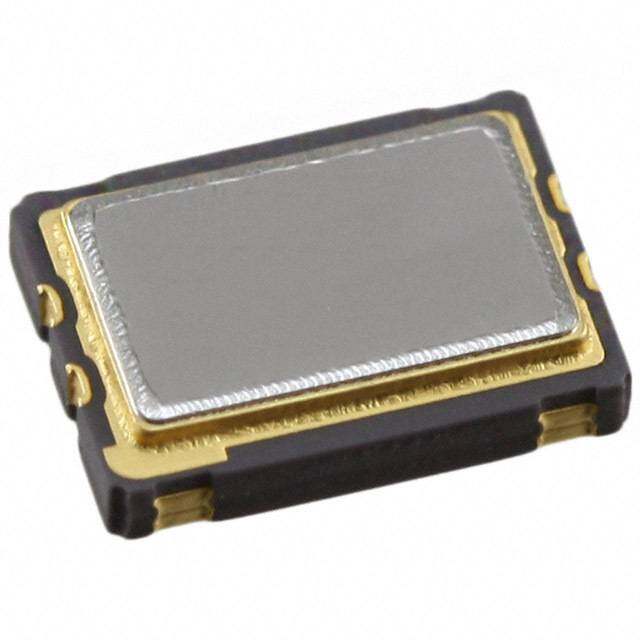
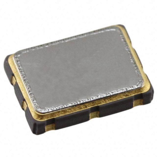
| 大小/尺寸 | 0.276" 长 x 0.197" 宽(7.00mm x 5.00mm) |
| 安装类型 | 表面贴装 |
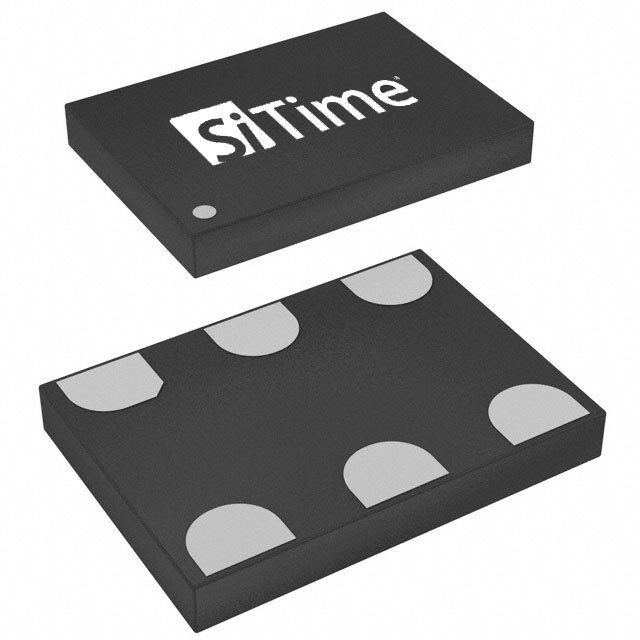
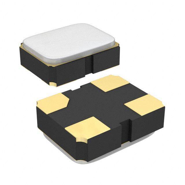
| 封装/外壳 | 6-SMD,无引线(DFN,LCC) |
| 工作温度 | -40°C ~ 85°C |
| 标准包装 | 1 |
| 电压-电源 | 3.3V |
| 电流-电源(最大值) | 33mA |
| 电流-电源(禁用)(最大值) | 70µA |
| 等级 | - |
| 类型 | MEMS(硅) |
| 输出 | LVCMOS,LVTTL |
| 频率 | 16.8MHz |
| 频率稳定度 | ±25ppm |
| 高度 | 0.039"(1.00mm) |


- 商务部:美国ITC正式对集成电路等产品启动337调查
- 曝三星4nm工艺存在良率问题 高通将骁龙8 Gen1或转产台积电
- 太阳诱电将投资9.5亿元在常州建新厂生产MLCC 预计2023年完工
- 英特尔发布欧洲新工厂建设计划 深化IDM 2.0 战略
- 台积电先进制程称霸业界 有大客户加持明年业绩稳了
- 达到5530亿美元!SIA预计今年全球半导体销售额将创下新高
- 英特尔拟将自动驾驶子公司Mobileye上市 估值或超500亿美元
- 三星加码芯片和SET,合并消费电子和移动部门,撤换高东真等 CEO
- 三星电子宣布重大人事变动 还合并消费电子和移动部门
- 海关总署:前11个月进口集成电路产品价值2.52万亿元 增长14.8%


PDF Datasheet 数据手册内容提取
SiT3807 Standard Frequency MEMS VCXO The Smart Timing Choice The Smart Timing Choice Features Applications 30 standard frequencies between 1.544 MHz and 49.152 MHz Telecom clock synchronization, instrumentation 100% pin-to-pin drop-in replacement to quartz-based VCXO Low bandwidth analog PLL, jitter cleaner, clock recovery, audio Frequency stability as tight as ±25 ppm Video, 3G/HD-SDI, FPGA, broadband and networking Widest pull range options from ±25 ppm to ±200 ppm Industrial or extended commercial temperature range Superior pull range linearity of ≤1%, 10 times better than quartz LVCMOS/LVTTL compatible output Four industry-standard packages: 2.5 mm x2.0 mm (4-pin), 3.2 mm x 2.5mm (4-pin), 5.0 mm x 3.2 mm (6-pin), 7.0 mm x 5.0 mm (6-pin) Instant samples with Time Machine II and field programmable oscillators RoHS and REACH compliant, Pb-free, Halogen-free and Antimony-free Electrical Specifications Table 1. Electrical Characteristics[1, 2, 3] Parameter Symbol Min. Typ. Max. Unit Condition Frequency Range Output Frequency Range f 1.544 – 49.152 MHz Refer to Table 11 for the exact list of supported frequencies Frequency Stability and Aging Frequency Stability F_stab -25 – +25 ppm Inclusive of Initial tolerance[4] at 25 °C, and variation over -50 – +50 ppm temperature, rated supply voltage and load. Aging F_aging -5 – +5 ppm 10 years, 25°C Operating Temperature Range T_use -20 – +70 °C Extended Commercial -40 – +85 °C Industrial Supply Voltage and Current Consumption Supply Voltage Vdd 1.71 1.8 1.89 V 2.25 2.5 2.75 V Additional supply voltages between 2.5V and 3.3V can be 2.52 2.8 3.08 V supported. Contact SiTime for additional information. 2.97 3.3 3.63 V Current Consumption Idd – 31 33 mA No load condition, f = 20 MHz, Vdd = 2.5V, 2.8V or 3.3V – 29 31 mA No load condition, f = 20 MHz, Vdd = 1.8V Standby Current I_std – – 70 A Vdd = 2.5V, 2.8V, 3.3V, ST = GND, output is Weakly Pulled Down – – 10 A Vdd = 1.8V, ST = GND, output is Weakly Pulled Down VCXO Characteristics Pull Range[5, 6] PR ±25, ±50, ±100, ±150, ±200 ppm See the Absolute Pull Range and APR table on page 10 Upper Control Voltage VC_U 1.7 – – V Vdd = 1.8V, Voltage at which maximum deviation is guaranteed. 2.4 – – V Vdd = 2.5V, Voltage at which maximum deviation is guaranteed. 2.7 – – V Vdd = 2.8V, Voltage at which maximum deviation is guaranteed. 3.2 – – V Vdd = 3.3V, Voltage at which maximum deviation is guaranteed. Lower Control Voltage VC_L – – 0.1 V Voltage at which minimum deviation is guaranteed. Control Voltage Input Impedance Z_in 100 – – kΩ Control Voltage Input Capacitance C_in – 5 – pF Linearity Lin – 0.1 1 % Frequency Change Polarity – Positive slope – Control Voltage Bandwidth (-3dB) V_BW – 8 – kHz Contact SiTime for 16 kHz and other high bandwidth options LVCMOS Output Characteristics Duty Cycle DC 45 – 55 % All Vdds. Refer to Note 11 for definition of Duty Cycle Rise/Fall Time Tr, Tf – 1.5 2 ns Vdd = 1.8V, 2.5v, 2.8V or 3.3V, 10% - 90% Vdd level Output High Voltage VOH 90% – – Vdd IOH = -7 mA (Vdd = 3.0V or 3.3V) IOH = -4 mA (Vdd = 2.8V or 2.5V) IOH = -2 mA (Vdd = 1.8V) Output Low Voltage VOL – – 10% Vdd IOL = 7 mA (Vdd = 3.0V or 3.3V) IOL = 4 mA (Vdd = 2.8V or 2.5V) IOL = 2 mA (Vdd = 1.8V) SiTime Corporation 990 Almanor Avenue, Sunnyvale, CA 94085 (408) 328-4400 www.sitime.com Rev. 1.01 Revised January 8, 2015
SiT3807 Standard Frequency MEMS VCXO The Smart Timing Choice TheSmartTimingChoice Electrical Specifications (continued) Table 1. Electrical Characteristics[1, 2, 3] Parameter Symbol Min. Typ. Max. Unit Condition Input Characteristics Input Pull-up Impedance Z_in – 100 250 kΩ For the OE/ST pin for 6-pin devices Input Capacitance C_in – 5 – PF For the OE/ST pin for 6-pin devices Startup and Resume Timing Startup Time T_start – – 10 ms See Figure 7 for startup resume timing diagram OE Enable/Disable Time T_oe – – 180 ns f = 40 MHz, all Vdds. For other freq, T_oe = 100 ns + 3 clock periods Resume Time T_resume – 7 10 ms See Figure 8 for resume timing diagram Jitter RMS Period Jitter T_jitt – 1.5 2 ps f = 20 MHz, Vdd = 2.5V, 2.8V or 3.3V – 2 3 ps f = 20 MHz, Vdd = 1.8V RMS Phase Jitter (random) T_phj – 0.5 1 ps f = 20 MHz, Integration bandwidth = 12 kHz to 20 MHz, All Vdds Notes: 1.All electrical specifications in the above table are specified with 15 pF output load and for all Vdd(s) unless otherwise stated. 2.The typical value of any parameter in the Electrical Characteristics table is specified for the nominal value of the highest voltage option for that parameter and at 25 °C temperature. 3.All max and min specifications are guaranteed across rated voltage variations and operating temperature ranges, unless specified otherwise 4.Initial tolerance is measured at Vin = Vdd/2 5.Absolute Pull Range (APR) is defined as the guaranteed pull range over temperature and voltage. 6.APR = pull range (PR) - frequency stability (F_stab) - Aging (F_aging) Rev. 1.01 Page 2 of 11 www.sitime.com
SiT3807 Standard Frequency MEMS VCXO The Smart Timing Choice TheSmartTimingChoice Table 2. Pin Description. 4-Pin Configuration (For 2.5 x 2.0 mm and 3.2 x 2.5 mm packages) Top View Pin Symbol Functionality 1 VIN Input 0-Vdd: produces voltage dependent frequency change VIN 1 4 VDD 2 GND Power Electrical ground 3 CLK Power Power supply voltage 4 VDD Input Oscillator output power[7] GND 2 3 CLK Power Note: Figure 1. 7. A capacitor value of 0.1 µF between VDD and GND is recommended. Table 3. Pin Description. 6-Pin Configuration (For 5.0 x 3.2 mm and 7.0 x 5.0 mm packages) Pin Symbol Functionality Top View 1 VIN Input 0-Vdd: produces voltage dependent frequency change No H or L or Open: No effect on output frequency or other device Connect functions Output H or Open[8]: specified frequency output VIN 1 6 VDD 2 NC/OE/ ST Enable L: output is high Standby H or Open[8]: specified frequency output NC/OE/ST 2 5 NC L: output is low (weak pull down)[9]. Oscillation stops 3 GND Power Electrical ground GND 3 4 CLK 4 CLK Output Oscillator output No H or L or Open: No effect on output frequency or other device 5 NC Connect functions Figure 2. 6 VDD Power Power supply voltage[10] Notes: 8. In OE or ST mode, a pull-up resistor of 10 kΩ or less is recommended if pin 2 in the 6-pin package is not externally driven. If pin 2 needs to be left floating, use the NC option 9. Typical value of the weak pull-down impedance is 5 mΩ 10. A capacitor value of 0.1 µF between VDD and GND is recommended. Table 4. Absolute Maximum Limits Attempted operation outside the absolute maximum ratings may cause permanent damage to the part. Actual performance of the IC is only guaranteed within the operational specifications, not at absolute maximum ratings. Parameter Min. Max. Unit Storage Temperature -65 150 °C VDD -0.5 4 V Electrostatic Discharge – 2000 V Soldering Temperature (follow standard Pb free soldering guidelines) – 260 °C Table 5. Thermal Consideration JA, 4 Layer Board JA, 2 Layer Board JC, Bottom Parameter (°C/W) (°C/W) (°C/W) 7050 191 263 30 5032 97 199 24 3225 109 212 27 2520 117 222 26 Table 6. Environmental Compliance Parameter Condition/Test Method Mechanical Shock MIL-STD-883F, Method 2002 Mechanical Vibration MIL-STD-883F, Method 2007 Temperature Cycle JESD22, Method A104 Solderability MIL-STD-883F, Method 2003 Moisture Sensitivity Level MSL1 @ 260°C Rev. 1.01 Page 3 of 11 www.sitime.com
SiT3807 Standard Frequency MEMS VCXO The Smart Timing Choice TheSmartTimingChoice Phase Noise Plot -100 -110 Integrated random phase jitter (RMS, 12kHz-5MHz): 0.52ps -120 z) H c/ dB -130 e ( s oi N -140 e s a h P -150 -160 -170 3 4 5 6 10 10 10 10 Frequency Offset (Hz) Figure 3. Phase Noise, 10 MHz, 3.3V, LVCMOS Output Test Circuit and Waveform Vdd Vout Vout Test Test Point Point 4 3 6 5 4 Power Power Supply 15pF Supply 15pF 0.1µF 0.1µF 1 2 (including probe 1 2 3 (including probe and fixture and fixture capacitance) capacitance) OE/ST Function OE/ST Function Vdd Vc Vc Figure 4. Test Circuit (4-Pin Device) Figure 5. Test Circuit (6-Pin Device) tr tf 90% Vdd 50% 10% Vdd High Pulse Low Pulse (TH) (TL) Period Figure 6. Waveform Note: 11.Duty Cycle is computed as Duty Cycle = TH/Period. 12.SiT3807 supports the configurable duty cycle feature. For custom duty cycle at any given frequency, contact SiTime. Rev. 1.01 Page 4 of 11 www.sitime.com
SiT3807 Standard Frequency MEMS VCXO The Smart Timing Choice TheSmartTimingChoice Timing Diagram 80% Vdd, 2.5/2.8/3.3V devices Vdd Vdd 80% Vdd, 1.8V devices 50% Vdd Pin 4 Voltage T_start No Glitch ST Voltage T_resume during start up CLK Output CLK Output T_start: Time to start from power-off T_resume: Time to resume from ST Figure 7. Startup Timing (OE/ST Mode) Figure 8. Standby Resume Timing (ST Mode Only) u Vdd Vdd 50% Vdd OE Voltage OE Voltage T_oe 50% Vdd T_oe CLK Output CLK Output HZ T_oe: Time to re-enable the clock output T_oe: Time to put the output in High Z mode Figure 9. OE Enable Timing (OE Mode Only) Figure 10. OE Disable Timing (OE Mode Only) Notes: 13. SiT3807 supports “no runt” pulses and “no glitch” output during startup or resume. 14. SiT3807 supports gated output which is accurate within rated frequency stability from the first cycle. Rev. 1.01 Page 5 of 11 www.sitime.com
SiT3807 Standard Frequency MEMS VCXO The Smart Timing Choice TheSmartTimingChoice Programmable Drive Strength The SiT3807 can support up to 60 pF maximum capacitive loads. Refer to the Rise/Tall Time Tables to determine the The SiT3807 includes a programmable drive strength feature proper drive strength for the desired combination of output to provide a simple, flexible tool to optimize the clock rise/fall load vs. rise/fall time time for specific applications. Benefits from the programmable drive strength feature are: SiT3807 Drive Strength Selection • Improves system radiated electromagnetic interference Tables 7 through 10 define the rise/fall times for a given capac- (EMI) by slowing down the clock rise/fall time itive load and supply voltage. • Improves the downstream clock receiver’s (RX) jitter by de- creasing (speeding up) the clock rise/fall time. 1.Select the table that matches the SiT3807 nominal supply voltage (1.8V, 2.5V, 2.8V, 3.3V). • Ability to drive large capacitive loads while maintaining full swing with sharp edge rates. 2.Select the capacitive load column that matches the appli- For more detailed information about rise/fall time control and cation requirement (5 pF to 60 pF) drive strength selection, see the SiTime Application Notes 3.Under the capacitive load column, select the desired section; http://www.sitime.com/support/application-notes. rise/fall times. 4.The left-most column represents the part number code for EMI Reduction by Slowing Rise/Fall Time the corresponding drive strength. Figure 11 shows the harmonic power reduction as the rise/fall 5.Add the drive strength code to the part number for ordering times are increased (slowed down). The rise/fall times are purposes. expressed as a ratio of the clock period. For the ratio of 0.05, the signal is very close to a square wave. For the ratio of 0.45, Calculating Maximum Frequency the signal is very close to near-triangular waveform. These Based on the rise and fall time data given in Tables 7 through results, for example, show that the 11th clock harmonic can be 10, the maximum frequency the oscillator can operate with reduced by 35 dB if the rise/fall edge is increased from 5% of guaranteed full swing of the output voltage over temperature the period to 45% of the period. can be calculated as follows: trise=0.05 1 10 ttrriissee==00..115 Max Frequency=3.5 x Trf_10/90 trise=0.2 0 trise=0.25 trise=0.3 dB) -10 ttrriissee==00..345 Where Trf_10/90 is the typical rise/fall time at 10% to 90% Vdd. e ( -20 trise=0.45 d mplitu -30 Example 1 a -40 armonic --6500 C•alVcdudla t=e 3fM.3AVX (fToar bthlee 1fo0l)lowing condition: H • Capacitive Load: 30 pF -70 • Typical Tr/f time = 1.66 ns (drive strength part number code -80 1 3 5 7 9 11 = G) Harmonic number Figure 11. Harmonic EMI reduction as a Function of Part number for the above example: Slower Rise/Fall Time SiT3807AIGG2-33EH-49.152000 Jitter Reduction with Faster Rise/Fall Time Power supply noise can be a source of jitter for the downstream chipset. One way to reduce this jitter is to Drive strength code is inserted here. Default setting is “-” increase rise/fall time (edge rate) of the input clock. Some chipsets would require faster rise/fall time in order to reduce their sensitivity to this type of jitter. Refer to the Rise/Fall Time Tables to determine the proper drive strength. High Output Load Capability The rise/fall time of the input clock varies as a function of the actual capacitive load the clock drives. At any given drive strength, the rise/fall time becomes slower as the output load increases. As an example, for a 3.3V SiT3807 device with default drive strength setting, the typical rise/fall time is 1.15ns for 15 pF output load. The typical rise/fall time slows down to 2.72ns when the output load increases to 45 pF. One can choose to speed up the rise/fall time to 1.41ns by then increasing the drive strength setting to P on the SiT3807. Rev. 1.01 Page 6 of 11 www.sitime.com
SiT3807 Standard Frequency MEMS VCXO The Smart Timing Choice TheSmartTimingChoice Rise/Fall Time (10% to 90%) vs C Tables LOAD Table 7. Vdd = 1.8V Rise/Fall Times for Specific CLOAD Table 8. Vdd = 2.5V Rise/Fall Times for Specific CLOAD Rise/Fall Time Typ (ns) Rise/Fall Time Typ (ns) Drive Strength \ CLOAD 5 pF 15 pF 30 pF 45 pF 60 pF Drive Strength \ CLOAD 5 pF 15 pF 30 pF 45 pF 60 pF L 12.45 17.68 19.48 46.21 57.82 L 8.68 13.59 18.36 32.70 42.06 A 6.50 10.27 16.21 23.92 30.73 A 4.42 7.18 11.93 16.60 21.38 R 4.38 7.05 11.61 16.17 20.83 R 2.93 4.78 8.15 11.19 14.59 B 3.27 5.30 8.89 12.18 15.75 B 2.21 3.57 6.19 8.55 11.04 S 2.62 4.25 7.20 9.81 12.65 S 1.67 2.87 4.94 6.85 8.80 D 2.19 3.52 6.00 8.31 10.59 D 1.50 2.33 4.11 5.68 7.33 T 1.76 3.01 5.14 7.10 9.15 T 1.06 2.04 3.50 4.84 6.26 E 1.59 2.59 4.49 6.25 7.98 E 0.98 1.69 3.03 4.20 5.51 U 1.49 2.28 3.96 5.55 7.15 U 0.93 1.48 2.69 3.73 4.92 F 1.22 2.10 3.57 5.00 6.46 F 0.90 1.37 2.44 3.34 4.42 W 1.07 1.88 3.23 4.50 5.87 W 0.87 1.29 2.21 3.04 4.02 G 1.01 1.64 2.95 4.12 5.40 G or "-": Default 0.67 1.20 2.00 2.79 3.69 X 0.96 1.50 2.74 3.80 4.98 X 0.44 1.10 1.86 2.56 3.43 K 0.92 1.41 2.56 3.52 4.64 K 0.38 0.99 1.76 2.37 3.18 Y 0.88 1.34 2.39 3.25 4.32 Y 0.36 0.83 1.66 2.20 2.98 Q 0.86 1.29 2.24 3.04 4.06 Q 0.34 0.71 1.58 2.07 2.80 Z or "-": Default 0.82 1.24 2.07 2.89 3.82 Z 0.33 0.65 1.51 1.95 2.65 M 0.77 1.20 1.94 2.72 3.61 M 0.32 0.62 1.44 1.85 2.50 N 0.66 1.15 1.84 2.58 3.41 N 0.31 0.59 1.37 1.77 2.39 P 0.51 1.09 1.76 2.45 3.24 P 0.30 0.57 1.29 1.70 2.28 Table 9. Vdd = 2.8V Rise/Fall Times for Specific CLOAD Table 10. Vdd = 3.3V Rise/Fall Times for Specific CLOAD Rise/Fall Time Typ (ns) Rise/Fall Time Typ (ns) Drive Strength \ CLOAD 5 pF 15 pF 30 pF 45 pF 60 pF Drive Strength \ CLOAD 5 pF 15 pF 30 pF 45 pF 60 pF L 7.93 12.69 17.94 30.10 38.89 L 7.18 11.59 17.24 27.57 35.57 A 4.06 6.66 11.04 15.31 19.80 A 3.61 6.02 10.19 13.98 18.10 R 2.68 4.40 7.53 10.29 13.37 R 2.31 3.95 6.88 9.42 12.24 B 2.00 3.25 5.66 7.84 10.11 B 1.65 2.92 5.12 7.10 9.17 S 1.59 2.57 4.54 6.27 8.07 S 1.43 2.26 4.09 5.66 7.34 D 1.19 2.14 3.76 5.21 6.72 D 1.01 1.91 3.38 4.69 6.14 T 1.00 1.79 3.20 4.43 5.77 T 0.94 1.51 2.86 3.97 5.25 E 0.94 1.51 2.78 3.84 5.06 E 0.90 1.36 2.50 3.46 4.58 U 0.90 1.38 2.48 3.40 4.50 U 0.86 1.25 2.21 3.03 4.07 F 0.87 1.29 2.21 3.03 4.05 F or "-": Default 0.48 1.15 1.95 2.72 3.65 W 0.62 1.19 1.99 2.76 3.68 W 0.38 1.04 1.77 2.47 3.31 G or "-": Default 0.41 1.08 1.84 2.52 3.36 G 0.36 0.87 1.66 2.23 3.03 X 0.37 0.96 1.72 2.33 3.15 X 0.34 0.70 1.56 2.04 2.80 K 0.35 0.78 1.63 2.15 2.92 K 0.33 0.63 1.48 1.89 2.61 Y 0.33 0.67 1.54 2.00 2.75 Y 0.32 0.60 1.40 1.79 2.43 Q 0.32 0.63 1.46 1.89 2.57 Q 0.32 0.58 1.31 1.69 2.28 Z 0.31 0.60 1.39 1.80 2.43 Z 0.30 0.56 1.22 1.62 2.17 M 0.30 0.57 1.31 1.72 2.30 M 0.30 0.55 1.12 1.54 2.07 N 0.30 0.56 1.22 1.63 2.22 N 0.30 0.54 1.02 1.47 1.97 P 0.29 0.54 1.13 1.55 2.13 P 0.29 0.52 0.95 1.41 1.90 Rev. 1.01 Page 7 of 11 www.sitime.com
SiT3807 Standard Frequency MEMS VCXO The Smart Timing Choice TheSmartTimingChoice Instant Samples with Time Machine and For more information regarding SiTime’s field programmable Field Programmable Oscillators solutions, visit http://www.sitime.com/time-machine and http://www.sitime.com/fp-devices. SiTime supports a field programmable version of the SiT3807 low power oscillator for fast prototyping and real time custom- SiT3807 is typically factory-programmed per customer ization of features. The field programmable devices (FP ordering codes for volume delivery. devices) are available for all four standard SiT3807 package sizes and can be configured to one’s exact specification using the Time Machine II, an USB powered MEMS oscillator programmer. Customizable Features of the SiT3807 FP Devices Include • 30standard frequencies • Two frequency stability options: ±25 ppm, ±50 ppm • Two operating temperatures: -20 to 70°C or -40 to 85°C • Four supply voltage options: 1.8V, 2.5V, 2.8V, and 3.3V • Five pull range options: ±25 ppm, ±50 ppm, ±100 ppm, ±150 ppm, ±200 ppm Rev. 1.01 Page 8 of 11 www.sitime.com
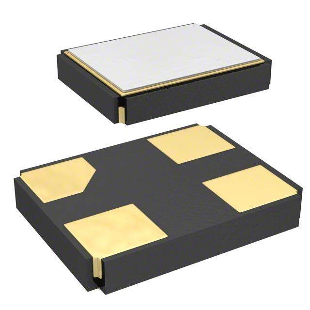
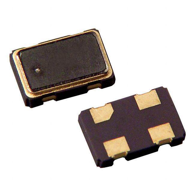
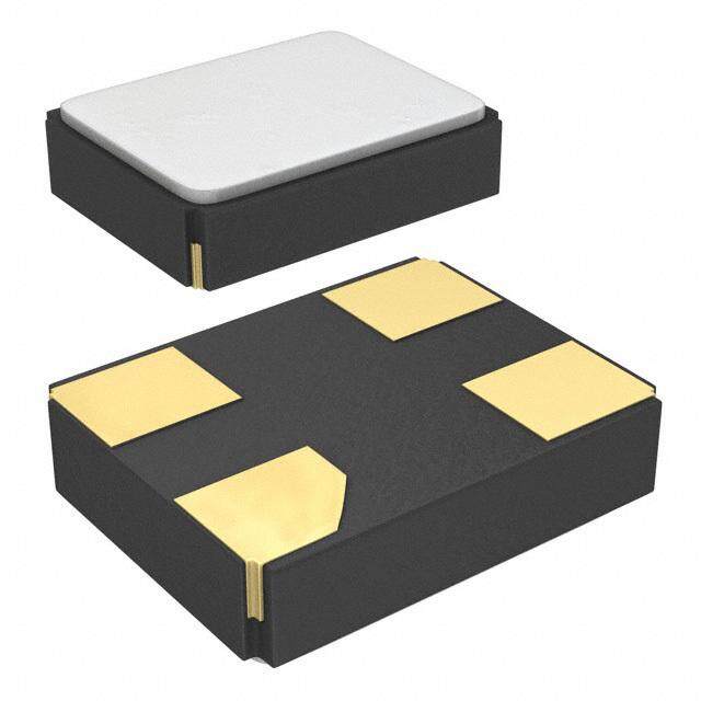
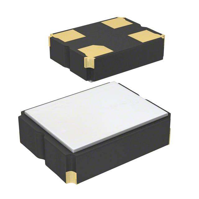
SiT3807 Standard Frequency MEMS VCXO The Smart Timing Choice TheSmartTimingChoice Dimensions and Patterns Package Size – Dimensions (Unit: mm)[15] Recommended Land Pattern (Unit: mm) 2.7 x 2.4 x 0.75 mm (100% compatible with 2.5 x 2. 0 mm footprint) 1.9 2.7 ± 0.05 1.00 YXXXX 2.4 ± 0.05 1.25 0.50 1.5 0.85 0 1. 0.75 ± 0.05 1.1 3.2 x 2.5 x 0.75 mm 2.2 3.2 ± 0.05 2.1 #4 #3 #3 #4 5 0 YXXXX 5 ± 0. 0.9 1.9 2. 0.7 2 #1 #2 #2 #1 1. 5 0.9 0.0 1.4 ± 5 7 0. 5.0 x 3.2 x 0.75 mm #6 #5 #4 #4 #5 #6 1.20 YXXXX #1 #2 #3 #3 #2 #1 0.75±0.05 7.0 x 5.0x 0.90 mm 7.0±0.10 5.08 5.08 #6 #5 #4 #4 #5 #6 YXXXX 5.0±0.10 2.60 1.10 80 3. #1 #2 #3 #3 #2 #1 0 1.40 1.6 0.90 ±0.10 1.60 Note: 15.Top marking: Y denotes manufacturing origin and XXXX denotes manufacturing lot number. The value of “Y” will depend on the assembly location of the device. Rev. 1.01 Page 9 of 11 www.sitime.com
SiT3807 Standard Frequency MEMS VCXO The Smart Timing Choice TheSmartTimingChoice Ordering Information SiT3807AC -22-33EH-49.152000D Packing Method Part Family “T”: 12 mm Tape & Reel, 3ku reel “SiT3807” “Y”: 12 mm Tape & Reel, 1ku reel “D”: 8 mm Tape & Reel, 3ku reel Revision Letter “E”: 8 mm Tape & Reel, 1ku reel “A” is the revision Blank for Bulk Temperature Range Frequency See Supported Frequencies Table “C” Commercial, -20 to 70ºC below “I” Industrial, -40 to 85ºC Pull Range Options Output Drive Strength “M” for ±25 ppm “–” Default (datasheet limits) “B” for ±50 ppm See rise/fall tables on page 7 “E” for ±100 ppm “L” “S” “U” “X” “Z” “G” for ±150 ppm “A” “D” “F” “K” “M” “H” for ±200 ppm “R” “T” “W” “Y” “N” “B” “E” “G” “Q” “P” Feature Pin Package “N” for No Connect in 6-pin devices, “G” 2.5 x 2.0 mm x mm Default value in 4-pin device “2” 4-pin, 3.2 x 2.5 mm x mm “E” for Output Enable (6-pin only) “C” 6-pin, 5.0 x 3.2 mm x mm “S” for Standby (6-pin only) “D” 6-pin, 7.0 x 5.0 mm x mm Supply Voltage Frequency Stability “18” for 1.8 V ±5% “2” for ±25 ppm “25” for 2.5 V ±10% “3” for ±50 ppm “28” for 2.8 V ±10% “33” for 3.3 V ±10% Table 11. Supported Frequencies 1.544000 MHz 4.096000 MHz 6.176000 MHz 8.000000 MHz 8.192000 MHz 10.000000 MHz 11.289600 MHz 12.288000 MHz 12.352000 MHz 13.500000 MHz 16.000000 MHz 16.348000 MHz 16.8 MHz 19.440000 MHz 20.000000 MHz 24.576000 MHz 24.700000 MHz 25.000000 MHz 25.576000 MHz 27.000000 MHz 30.000000 MHz 31.720000 MHz 32.000000 MHz 32.768000 MHz 35.328000 MHz 38.880000 MHz 39.322000 MHz 40.000000 MHz 44.736000 MHz 49.152000 MHz Table 12. APR Definition Absolute pull range (APR) = Norminal pull range (PR) - frequency stability (F_stab) - Aging (F_aging) APR Frequency Stability Nominal Pull Range ± 25 ± 50 APR (PPM) ± 25 – – ± 50 ± 20 – ± 100 ± 70 ± 45 ± 150 ± 120 ± 95 ± 200 ± 170 ± 145 Table 13. Ordering Codes for Supported Tape & Reel Packing Method[16] Device Size 12 mm T&R (3ku) 12 mm T&R (1ku) 8 mm T&R (3ku) 8 mm T&R (1ku) 2.5 x 2.0 mm – – D E 3.2 x 2.5 mm – – D E 5.0 x 3.2 mm T Y – – 7.0 x 5.0 mm T Y – – Note: 16.“–” indicates “not available.” Rev. 1.01 Page 10 of 11 www.sitime.com
SiT3807 Standard Frequency MEMS VCXO The Smart Timing Choice The Smart Timing Choice Table 14. Additional Information Document Description Download Link Manufacturing Tape & Reel dimension, http://www.sitime.com/component/docman/doc_download/85-manufaturing-notes-for-sitime-oscillators Notes reflow profile and other manufacturing related info Qualification RoHS report, reliability reports, http://www.sitime.com/support/quality-and-reliability Reports composition reports Performance Additional performance data http://www.sitime.com/support/performance-measurement-report Reports such as phase noise, current consumption and jitter for selected frequencies Termination Termination design http://www.sitime.com/support/application-notes Techniques recommendations Layout Techniques Layout recommendations http://www.sitime.com/support/application-notes VCXO Definition of key VCXO http://www.sitime.com/support2/documents/AN10020_VCXO_SpecDefinitions_rev1.pdf Specifications specifications such as APR and Kv VCXO in PLL Selection of VCXO parameters http://www.sitime.com/support2/documents/AN10021_VCXO_PLL_Design_Guidelines_1v0.pdf Design and trade-offs in PLL designs Revision History Table 15. Datasheet Version and Change Log Version Release Date Change Summary 0.6 1/24/2013 Preliminary 1.0 1/18/14 • Updated features and application • Updated electrical specifications table • Updated figure 4, • Added new 6-pin device for figure 5 • Updated timing diagrams • Updated programmable drive strength section • Updated ordering information drawing • Updated APR table • Updated ordering codes for tape and reel table • Reformatted additional information table columns 1.01 1/8/15 • Corrected CLK and VDD functionality description in Table 2 • Revised VIN functionality description in Table 3 © SiTime Corporation 2015. The information contained herein is subject to change at any time without notice. SiTime assumes no responsibility or liability for any loss, damage or defect of a Product which is caused in whole or in part by (i) use of any circuitry other than circuitry embodied in a SiTime product, (ii) misuse or abuse including static discharge, neglect or accident, (iii) unauthorized modification or repairs which have been soldered or altered during assembly and are not capable of being tested by SiTime under its normal test conditions, or (iv) improper installation, storage, handling, warehousing or transportation, or (v) being subjected to unusual physical, thermal, or electrical stress. Disclaimer: SiTime makes no warranty of any kind, express or implied, with regard to this material, and specifically disclaims any and all express or implied warranties, either in fact or by operation of law, statutory or otherwise, including the implied warranties of merchantability and fitness for use or a particular purpose, and any implied warranty arising from course of dealing or usage of trade, as well as any common-law duties relating to accuracy or lack of negligence, with respect to this material, any SiTime product and any product documentation. Products sold by SiTime are not suitable or intended to be used in a life support application or component, to operate nuclear facilities, or in other mission critical applications where human life may be involved or at stake. All sales are made conditioned upon compliance with the critical uses policy set forth below. CRITICAL USE EXCLUSION POLICY BUYER AGREES NOT TO USE SITIME'S PRODUCTS FOR ANY APPLICATION OR IN ANY COMPONENTS USED IN LIFE SUPPORT DEVICES OR TO OPERATE NUCLEAR FACILITIES OR FOR USE IN OTHER MISSION-CRITICAL APPLICATIONS OR COMPONENTS WHERE HUMAN LIFE OR PROPERTY MAY BE AT STAKE. SiTime owns all rights, title and interest to the intellectual property related to SiTime's products, including any software, firmware, copyright, patent, or trademark. The sale of SiTime products does not convey or imply any license under patent or other rights. SiTime retains the copyright and trademark rights in all documents, catalogs and plans supplied pursuant to or ancillary to the sale of products or services by SiTime. Unless otherwise agreed to in writing by SiTime, any reproduction, modification, translation, compilation, or representation of this material shall be strictly prohibited. Rev. 1.01 Page 11 of 11 www.sitime.com
The Smart Timing Choice The Smart Timing Choice Supplemental Information The Supplemental Information section is not part of the datasheet and is for informational purposes only. SiTime Corporation 990 Almanor Avenue, Sunnyvale, CA 94085 (408) 328-4400 www.sitime.com
The Smart Timing Choice The Smart Timing Choice Silicon MEMS Outperforms Quartz SiTime Corporation 990 Almanor Avenue, Sunnyvale, CA 94085 (408) 328-4400 www.sitime.com Silicon MEMS Outperforms Quartz Rev. 1.1 Revised October 5, 2013
Silicon MEMS Outperforms Quartz The Smart Timing Choice The Smart Timing Choice Best Reliability Best Electro Magnetic Susceptibility (EMS) Silicon is inherently more reliable than quartz. Unlike quartz SiTime’s oscillators in plastic packages are up to 54 times suppliers, SiTime has in-house MEMS and analog CMOS more immune to external electromagnetic fields than quartz expertise, which allows SiTime to develop the most reliable oscillators as shown in Figure 3. products. Figure 1 shows a comparison with quartz Why is SiTime Best in Class: technology. • Internal differential architecture for best common mode Why is SiTime Best in Class: noise rejection • SiTime’s MEMS resonators are vacuum sealed using an • Electrostatically driven MEMS resonator is more immune advanced EpiSeal™ process, which eliminates foreign par- to EMS ticles and improves long term aging and reliability • World-class MEMS and CMOS design expertise SiTime vs Quartz Mean Time Between Failure (Million Hours) Electro Magnetic Susceptibility (EMS) - 30 SiTime 500 B) - 40 - 39 - 40 - 42 - 43 - 45 d IDT (Fox) 38 SiTime (s - 50 r 20X Better u Epson 28 pS - 60 54SXi TBimeteter e g a - 70 - 73 TXC 16 re v A - 80 Pericom 14 - 90 0 200 400 600 Kyocera Epson TXC CW SiLabs SiTime Figure 1. Reliability Comparison[1] Figure 3. Electro Magnetic Susceptibility (EMS)[3] Best Aging Best Power Supply Noise Rejection Unlike quartz, MEMS oscillators have excellent long term SiTime’s MEMS oscillators are more resilient against noise on aging performance which is why every new SiTime product the power supply. A comparison is shown in Figure 4. specifies 10-year aging. A comparison is shown in Figure 2. Why is SiTime Best in Class: Why is SiTime Best in Class: • On-chip regulators and internal differential architecture for • SiTime’s MEMS resonators are vacuum sealed using an common mode noise rejection advanced EpiSeal process, which eliminates foreign parti- • Best analog CMOS design expertise cles and improves long term aging and reliability • Inherently better immunity of electrostatically driven MEMS resonator SiTime MEMS vs. Quartz Aging p-p Power Supply Noise Rejection V SiTIme NDK Epson Kyocera SiTime MEMS Oscillator Quartz Oscillator m 5.0 10 r e p PM) 68 2XS iBTiemttee r 8.0 r ettiJ eas)vm/sp(e s34..00 Aging (±P 24 1.5 3.0 3.5 hP detargetn IeioN detecnjI 12..00 3XS iBTSiemitTteiemre 0 vtidi 0.010 100 1,000 10,000 1-Year 10-Year dA Power Supply Noise Frequency (kHz) Figure 2. Aging Comparison[2] Figure 4. Power Supply Noise Rejection[4] Silicon MEMS Outperforms Quartz Rev. 1.1 www.sitime.com
Silicon MEMS Outperforms Quartz The Smart Timing Choice The Smart Timing Choice Best Vibration Robustness Best Shock Robustness High-vibration environments are all around us. All electronics, SiTime’s oscillators can withstand at least 50,000 g shock. from handheld devices to enterprise servers and storage They all maintain their electrical performance in operation systems are subject to vibration. Figure 5 shows a comparison during shock events. A comparison with quartz devices is of vibration robustness. shown in Figure 6. Why is SiTime Best in Class: Why is SiTime Best in Class: • The moving mass of SiTime’s MEMS resonators is up to • The moving mass of SiTime’s MEMS resonators is up to 3000 times smaller than quartz 3000 times smaller than quartz • Center-anchored MEMS resonator is the most robust • Center-anchored MEMS resonator is the most robust design design Vibration Sensitivity vs. Frequency Differential XO Shock Robustness -500 g 16 SiTime TXC Epson Connor Winfield Kyocera SiLabs M) 14.3 g) 100.00 PP 14 12.6 vity (ppb/ 10.00 eviation ( 1102 siti y D 8 ation Sen 1.00 USpBi eTtotitm e3re0 x Frequenc 46 3.9 2.9 2.5 USpBi eTtotitm e2re5 x br k 2 Vi 0.10 Pea 0 0.6 10 100 1000 Vibration Frequency (Hz) Kyocera Epson TXC CW SiLabs SiTime Figure 5. Vibration Robustness[5] Figure 6. Shock Robustness[6] Notes: 1. Data Source: Reliability documents of named companies. 2. Data source: SiTime and quartz oscillator devices datasheets. 3. Test conditions for Electro Magnetic Susceptibility (EMS): • According to IEC EN61000-4.3 (Electromagnetic compatibility standard) • Field strength: 3V/m • Radiated signal modulation: AM 1 kHz at 80% depth • Carrier frequency scan: 80 MHz – 1 GHz in 1% steps • Antenna polarization: Vertical • DUT position: Center aligned to antenna Devices used in this test: SiTime, SiT9120AC-1D2-33E156.250000 - MEMS based - 156.25 MHz Epson, EG-2102CA 156.2500M-PHPAL3 - SAW based - 156.25 MHz TXC, BB-156.250MBE-T - 3rd Overtone quartz based - 156.25 MHz Kyocera, KC7050T156.250P30E00 - SAW based - 156.25 MHz Connor Winfield (CW), P123-156.25M - 3rd overtone quartz based - 156.25 MHz SiLabs, Si590AB-BDG - 3rd overtone quartz based - 156.25 MHz 4. 50 mV pk-pk Sinusoidal voltage. Devices used in this test: SiTime, SiT8208AI-33-33E-25.000000, MEMS based - 25 MHz NDK, NZ2523SB-25.6M - quartz based - 25.6 MHz Kyocera, KC2016B25M0C1GE00 - quartz based - 25 MHz Epson, SG-310SCF-25M0-MB3 - quartz based - 25 MHz 5. Devices used in this test: same as EMS test stated in Note 3. 6. Test conditions for shock test: • MIL-STD-883F Method 2002 • Condition A: half sine wave shock pulse, 500-g, 1ms • Continuous frequency measurement in 100 μs gate time for 10 seconds Devices used in this test: same as EMS test stated in Note 3 7.Additional data, including setup and detailed results, is available upon request to qualified customers. Please contact productsupport@sitime.com. Silicon MEMS Outperforms Quartz Rev. 1.1 www.sitime.com
Document Feedback Form The Smart Timing Choice The Smart Timing Choice SiTime values your input in improving our documentation. Click here for our online feedback form or fill out and email the form below to productsupport@sitime.com. 1. Does the Electrical Characteristics table provide complete information? Yes No If No, what parameters are missing? _________________________________________________________________________________________________ 2. Is the organization of this document easy to follow? Yes No If “No,” please suggest improvements that we can make: _________________________________________________________________________________________________ 3. Is there any application specific information that you would like to see in this document? (Check all that apply) EMI Termination recommendations Shock and vibration performance Other If “Other,” please specify: _________________________________________________________________________________________________ 4. Are there any errors in this document? Yes No If “Yes”, please specify (what and where): _________________________________________________________________________________________________ 5. Do you have additional recommendations for this document? _________________________________________________________________________________________________ Name ________________________________________________________________________________ Title ________________________________________________________________________________ Company_________________________________________________________________________________________ Address _________________________________________________________________________________________ City / State or Province / Postal Code / Country ___________________________________________________________ Telephone __________________________________ Application________________________________________________________________________________________ Would you like a reply? Yes No Thank you for your feedback. Please click the email icon in your Adobe Reader tool bar and send to productsupport@sitime.com. Or you may use our online feedback form. Feedback Form Rev. 1.0 www.sitime.com