ICGOO在线商城 > 集成电路(IC) > PMIC - 全,半桥驱动器 > SIC769CD-T1-E3
 Datasheet下载
- 型号: SIC769CD-T1-E3
- 制造商: Vishay
- 库位|库存: xxxx|xxxx
- 要求:
| 数量阶梯 | 香港交货 | 国内含税 |
| +xxxx | $xxxx | ¥xxxx |
查看当月历史价格
查看今年历史价格
SIC769CD-T1-E3产品简介:
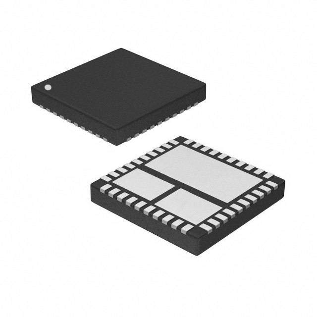
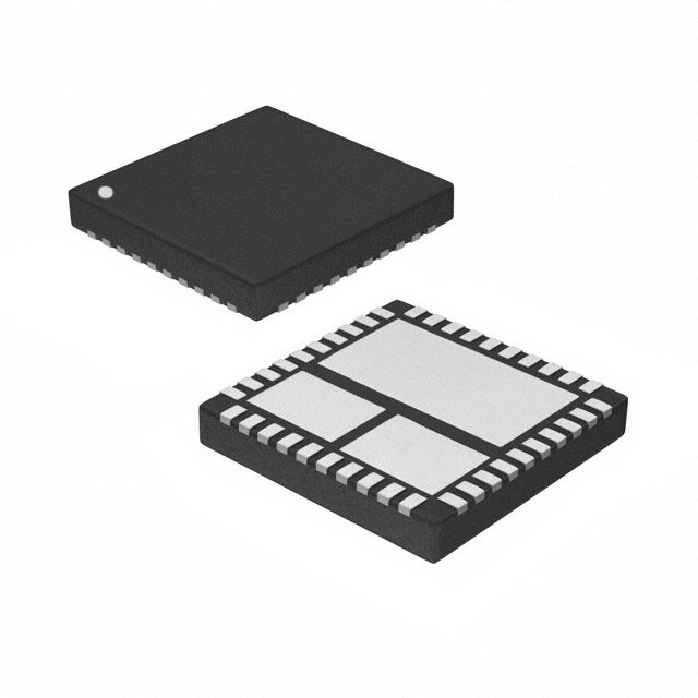
ICGOO电子元器件商城为您提供SIC769CD-T1-E3由Vishay设计生产,在icgoo商城现货销售,并且可以通过原厂、代理商等渠道进行代购。 SIC769CD-T1-E3价格参考¥28.75-¥32.34。VishaySIC769CD-T1-E3封装/规格:PMIC - 全,半桥驱动器, Half Bridge Driver Synchronous Buck Converters DrMOS PowerPAK® MLP66-40。您可以下载SIC769CD-T1-E3参考资料、Datasheet数据手册功能说明书,资料中有SIC769CD-T1-E3 详细功能的应用电路图电压和使用方法及教程。
Vishay Siliconix 的 SIC769CD-T1-E3 是一款半桥驱动器,属于电源管理集成电路(PMIC)的一部分,常用于需要高效功率转换和控制的应用场景。该器件主要应用于以下领域:

1. 电源转换系统:如DC-DC转换器、AC-DC电源适配器等,适用于需要高效率、高频开关性能的电源设计。

2. 电机驱动:用于无刷直流电机(BLDC)或永磁同步电机(PMSM)的驱动控制,常见于工业自动化、电动工具和家用电器中。

3. 照明系统:例如LED照明驱动电源,特别是在需要调光或高效能电源管理的场合。

4. 汽车电子:包括车载充电系统、DC-DC转换模块、电机控制等,满足汽车应用中对可靠性和效率的高要求。

5. 工业控制设备:如伺服驱动器、变频器和不间断电源(UPS),适用于需要高集成度和稳定性的工业环境。

SIC769CD-T1-E3 支持高侧和低侧MOSFET驱动,具备较强的抗干扰能力和保护功能,适合在高频、高效率的功率变换系统中使用。
| 参数 | 数值 |
| 产品目录 | 集成电路 (IC)半导体 |
| 描述 | IC CTLR PFC STAGE PPAK MLP66-40门驱动器 35A 3.0-16.0V Built-In PWM Cont |
| 产品分类 | PMIC - MOSFET,电桥驱动器 - 内部开关集成电路 - IC |
| 品牌 | Vishay SiliconixVishay / Siliconix |
| 产品手册 | |
| 产品图片 |
|
| rohs | 符合RoHS无铅 / 符合限制有害物质指令(RoHS)规范要求 |
| 产品系列 | 电源管理 IC,门驱动器,Vishay / Siliconix SIC769CD-T1-E3DrMOS |
| 数据手册 | |
| 产品型号 | SIC769CD-T1-E3SIC769CD-T1-E3 |
| 上升时间 | 8 ns |
| 下降时间 | 8 ns |
| 产品 | MOSFET Gate Drivers |
| 产品种类 | 门驱动器 |
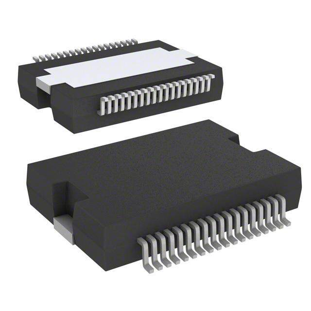
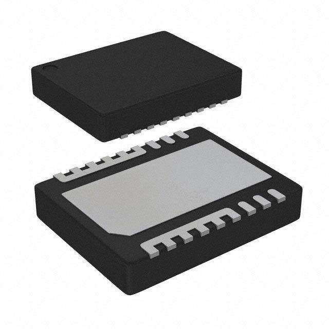
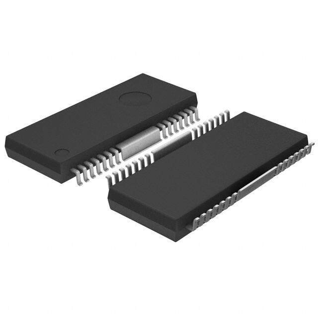
| 供应商器件封装 | PowerPAK® MLP66-40 |
| 其它名称 | SIC769CD-T1-E3DKR |
| 包装 | Digi-Reel® |
| 商标 | Vishay / Siliconix |
| 安装类型 | 表面贴装 |
| 安装风格 | SMD/SMT |
| 导通电阻 | - |
| 封装 | Reel |
| 封装/外壳 | PowerPAK® MLP66-40 |
| 封装/箱体 | PowerPAK MLP 66-40 |
| 工作温度 | -40°C ~ 125°C |
| 工厂包装数量 | 3000 |
| 最大工作温度 | + 125 C |
| 最小工作温度 | - 40 C |
| 标准包装 | 1 |
| 激励器数量 | 2 Driver |
| 特色产品 | http://www.digikey.cn/product-highlights/zh/sic769sic769asic762-integrated-solutions-drmos/50330 |
| 电压-电源 | 3 V ~ 16 V |
| 电流-峰值输出 | - |
| 电流-输出/通道 | 35A |
| 电源电压-最大 | 16 V |
| 电源电压-最小 | 3 V |
| 电源电流 | 0.4 mA |
| 类型 | Non-Inverting高端/低端驱动器 |
| 视频文件 | http://www.digikey.cn/classic/video.aspx?PlayerID=1364138032001&width=640&height=505&videoID=2318583557001 |
| 输入类型 | PWM |
| 输出数 | 1 |
| 输出电压 | 0.8 V to 2 V |
| 输出电流 | 30 A |
| 零件号别名 | SIC769CD-E3 |


- 商务部:美国ITC正式对集成电路等产品启动337调查
- 曝三星4nm工艺存在良率问题 高通将骁龙8 Gen1或转产台积电
- 太阳诱电将投资9.5亿元在常州建新厂生产MLCC 预计2023年完工
- 英特尔发布欧洲新工厂建设计划 深化IDM 2.0 战略
- 台积电先进制程称霸业界 有大客户加持明年业绩稳了
- 达到5530亿美元!SIA预计今年全球半导体销售额将创下新高
- 英特尔拟将自动驾驶子公司Mobileye上市 估值或超500亿美元
- 三星加码芯片和SET,合并消费电子和移动部门,撤换高东真等 CEO
- 三星电子宣布重大人事变动 还合并消费电子和移动部门
- 海关总署:前11个月进口集成电路产品价值2.52万亿元 增长14.8%

PDF Datasheet 数据手册内容提取
SiC769 Vishay Siliconix Integrated DrMOS Power Stage DESCRIPTION • FEATURES The SiC769CD is an integrated solution that contains PWM (cid:129) Integrated Gen III MOSFETs and DrMOS optimized n-channel MOSFETs (high side and low side) and compliant gate driver IC a full featured MOSFET driver IC. The device complies with (cid:129) Enables V switching at 1 MHz core the Intel DrMOS standard for desktop and server Vcore power (cid:129) Easily achieve > 90 % efficiency in multi-phase, stages. The SiC769CD delivers up to 35 A continuous output low output voltage solutions current and operates from an input voltage range of 3 V to (cid:129) Low ringing on the VSWH pin reduces EMI 16 V. The integrated MOSFETs are optimized for output (cid:129) Pin compatible with DrMOS 6 x 6 version 3.0 voltages in the ranges of 0.8 V to 2 V with a nominal input (cid:129) Tri-state PWM input function prevents negative output voltage of 12 V. The device can also deliver very high power voltage swing at 5 V output for ASIC applications. (cid:129) 5 V logic levels on PWM The SiC769CD incorporates an advanced MOSFET gate (cid:129) MOSFET threshold voltage optimized for 5 V driver bias driver IC. This IC accepts a single PWM input from the V R supply controller and converts it into the high side and low side (cid:129) Automatic skip mode operation (SMOD) for light load MOSFET gate drive signals. The driver IC is designed to efficiency implement the skip mode (SMOD) function for light load (cid:129) Under-voltage lockout efficiency improvement. Adaptive dead time control also (cid:129) Built-in bootstrap schottky diode works to improve efficiency at all load points. The SiC769CD has a thermal warning (THDN) that alerts the system of (cid:129) Adaptive deadtime and shoot through protection excessive junction temperature. The driver IC includes an (cid:129) Thermal shutdown warning flag enable pin, UVLO and shoot through protection. (cid:129) Low profile, thermally enhanced PowerPAK® MLP 6 x 6 The SiC769CD is optimized for high frequency buck 40 pin package applications. Operating frequencies in excess of 1 MHz can • Halogen-free according to IEC 61249-2-21 definition easily be achieved. (cid:129) Compliant to RoHS Directive 2002/95/EC The SiC769CD is packaged in Vishay Siliconix high performance PowerPAK MLP6 x 6 package. Compact APPLICATIONS co-packaging of components helps to reduce stray (cid:129) CPU and GPU core voltage regulation inductance, and hence increases efficiency. (cid:129) Server, computer, workstation, game console, graphics boards, PC SiC769CD APPLICATION DIAGRAMM 5 V VIN V D G V RV H IN VCIN SMOD BOOT G Controlle PWM PDWSBML# ate Driver PVHSWAHSE VO r THDN SiC769CD C P G G G ND L ND Figure 1 Document Number: 64981 www.vishay.com S11-0975-Rev. F, 16-May-11 1 This document is subject to change without notice. THE PRODUCTS DESCRIBED HEREIN AND THIS DOCUMENT ARE SUBJECT TO SPECIFIC DISCLAIMERS, SET FORTH AT www.vishay.com/doc?91000
SiC769 Vishay Siliconix ORDERING INFORMATION Part Number Package SiC769CD-T1-E3 PowerPAK MLP66-40 SiC769DB Reference board ABSOLUTE MAXIMUM RATINGS (T = 25 °C, unless otherwise noted) A Parameter Symbol Min. Max. Unit Input Voltage VIN - 0.3 20 Switch Node Voltage (DC) VSW - 0.3 20 Drive Input Voltage VDRV - 0.3 7 Control Input Voltage VCIN - 0.3 7 V , V , Logic Pins VPWM, VDSBL# - 0.3 VCIN + 0.3 V THDN SMOD Boot Voltage DC (referenced to CGND) - 0.3 27 V BS Boot Voltage < 200 ns Transient (referenced to CGND) - 0.3 29 Boot to Phase Voltage DC - 0.3 7 V BS_PH Boot to Phase Voltage < 200 ns - 0.3 9 Ambient Temperature Range TA - 40 125 Maximum Junction Temperature TJ 150 Storage Junction Temperature TSTG - 65 150 °C Soldering Peak Temperature 260 Note: a.T = 25 °C and all voltages referenced to P = C unless otherwise noted. A GND GND Stresses beyond those listed under "Absolute Maximum Ratings" may cause permanent damage to the device. These are stress ratings only, and functional operation of the device at these or any other conditions beyond those indicated in the operational sections of the specifications is not implied. Exposure to absolute maximum rating/conditions for extended periods may affect device reliability. RECOMMENDED OPERATING CONDITIONS Parameter Symbol Min. Typ. Max. Unit Input Voltage V 3 12 16 IN Control Input Voltage V 4.5 5.5 CIN V Drive Input Voltage V 4.5 5.5 DRV Switch Node V 12 16 SW_DC Note: a.Recommended operating conditions are specified over the entire temperature range, and all voltages referenced to P = C unless GND GND otherwise noted. THERMAL RESISTANCE RATINGS Parameter Symbol Typ. Max. Unit Maximum Power Dissipation at T = 25 °C P 25 PCB D_25C W Maximum Power Dissipation at T = 100 °C P 10 PCB D_100C Thermal Resistance from Junction to Top R 15 th_J_TOP °C/W Thermal Resistance from Junction to PCB R 5 th_J_PCB www.vishay.com Document Number: 64981 2 S11-0975-Rev. F, 16-May-11 This document is subject to change without notice. THE PRODUCTS DESCRIBED HEREIN AND THIS DOCUMENT ARE SUBJECT TO SPECIFIC DISCLAIMERS, SET FORTH AT www.vishay.com/doc?91000
SiC769 Vishay Siliconix ELECTRICAL SPECIFICATIONS Test Conditions Unless Specified V = V = 5 V, DSBL# SMOD V = 12 V, V = V 5 V, IN VDRV VCIN Parameter Symbol T = 25 °C Min. Typ.a Max. Unit A Power Supplies V = 0 V, no switching 20 DSBL# V Control Input Current I V = 5 V, no switching 400 µA CIN VCIN DSBL# V = 5 V, f = 300 kHz, D = 0.1 600 DSBL# s f = 300 kHz, D = 0.1 11 16 Drive Input Current (Dynamic) I s mA VDRV f = 1000 kHz, D = 0.1 40 54 s Bootstrap Supply Bootstrap Switch Forward Voltage V V = 5 V, forward bias current 2 mA 0.60 0.75 V BS Diode VCIN Control Inputs (PWM, DSBL#, SMOD) PWM Rising Threshold V 3.5 3.8 4.2 th_pwm_r PWM Falling Threshold V 0.8 1.0 1.2 th_pwm_f V PWM Tristate Rising Threshold V 0.9 1.3 1.8 th_tri_r PWM Tristate Falling Threshold V 3.4 3.7 4.0 th_tri_f PWM Tristate Rising Threshold Hysteresis V 200 hys_tri_r mV PWM Tristate Falling Threshold Hysteresis V 300 hys_tri_f Tristate Hold-Off Timeb t 150 ns TSHO V = 5 V 250 PWM Input Current I PWM µA PWM V = 0 V - 250 PWM V Rising (low to high) 2 SMOD, DSBL# Logic Input Voltage LOGIC_LH V V Falling (high to low) 0.8 LOGIC_LH Pull Down Impedance R 40 THDN 5 k resistor pull-up to V THDN Output Low V CIN 0.04 V THDNL Protection Thermal Warning Flag Set 150 Thermal Warning Flag Clear 135 °C Thermal Warning Flag Hysteresis 15 Under Voltage Lockout Rising, on threshold 3.3 3.9 V V Under Voltage Lockout UVLO Falling, off threshold 2.5 2.9 Under Voltage Lockout Hysteresis V 400 mV UVLO_HYST High Side Gate Discharge Resistorb R V = V = 0 V; V = 12 V 20.2 k HS_DSCRG VDRV VCIN IN Notes: a.Typical limits are established by characterization and are not production tested. b.Guaranteed by design. Document Number: 64981 www.vishay.com S11-0975-Rev. F, 16-May-11 3 This document is subject to change without notice. THE PRODUCTS DESCRIBED HEREIN AND THIS DOCUMENT ARE SUBJECT TO SPECIFIC DISCLAIMERS, SET FORTH AT www.vishay.com/doc?91000
SiC769 Vishay Siliconix MOSFET SPECIFICATIONS Test Conditions Unless Specified V = V = 5 V, VCIN DSBL# Parameter Symbol V = 12 V, T = 25 °C Min. Typ.a Max. Unit VIN A V V = 0, I = 250 µA 20 V DS GS DS High Side V = 5 V, resistance measured R GH 6 m DS(on)_H at package pins V V = 0, I = 250 µA 20 V DS GS DS Low Side V = 5 V, resistance measured R GL 1.7 m DS(on)_L at package pins Note: a. Typical MOSFET Parameters are provided as a design guide. TIMING SPECIFICATIONS Test Conditions Unless Specified V = V = V = 5 V, VDRV VCIN DSBL# Parameter Symbol V = 12 V, T = 25 °C Min. Typ. Max. Unit VIN A Turn Off Propagation Delay t 25 % of PWM to 90 % of GH 10 20 30 High Sidea d_on_HS Rise Time High Side t 10 % to 90 % of GH 8 r_HS Fall Time High Side t 90 % to 10 % of GH 8 f_HS Turn Off Propagation Delay Low Sidea td_off_LS 75 % of PWM to 90 % of GL 10 20 30 ns Rise Time Low Side t 10 % to 90 % of GL 8 r_LS Fall Time Low Side t 90 % to 10 % of GL 8 f_LS Dead Time Rising t 10 % of GL to 10 % of GH 15 dead_on Dead Time Falling t 10 % of GH to 10 % of GL 15 dead_off Note: a. Min. and Max. are not 100 % production tested. www.vishay.com Document Number: 64981 4 S11-0975-Rev. F, 16-May-11 This document is subject to change without notice. THE PRODUCTS DESCRIBED HEREIN AND THIS DOCUMENT ARE SUBJECT TO SPECIFIC DISCLAIMERS, SET FORTH AT www.vishay.com/doc?91000
SiC769 Vishay Siliconix TIMING DEFINITIONS PWM 75% 25% GH 90% 90% GL 10% 10% SW 1 2 3 4 5 6 7 8 Region Definition Symbol 1 Turn off propagation delay LS t d_off_LS 2 Fall time LS t f_LS 3 Dead time rising t dead_on 4 Rise time HS t r_HS 5 Turn off propagation delay HS t d_off_HS 6 Fall time HS t f_HS 7 Dead time falling t dead_off 8 Rise time LS t r_LS Note: GH is referenced to the high side source. GL is referenced to the low side source. SiC769CD BLOCK DIAGRAM THTDHDNN VVDDRRVV BBOOOOTT GGHH Thermal MoThnerimtoalr and WarnMWionanrigntoinrg& VVININ VCVICNIN UUVVLLOO DSBDSLB#L# 2020KK VVCCININ -- VVSSWWHH PLWogMic CAronstis-- ++ Vref=1V PWPWMM aMCnSPtaodaCWtcen oMSnMhttrrLtaoioaonclgh<eii cnee CoCnCLoCAodononntntugir-tdoCrcuilroccLottoisiloo sgn-icn +-+- LLGG VREFV=DVD R1RVV V VVreRf=E1VF= 1 V CGCNGDND Zero- ZCeruo-rCruerrnentt Dectect Detect -- VVSWSHWH ++ PPGNGDND PGPNGDND SMOD# GL SMOD# GL Figure 2 Document Number: 64981 www.vishay.com S11-0975-Rev. F, 16-May-11 5 This document is subject to change without notice. THE PRODUCTS DESCRIBED HEREIN AND THIS DOCUMENT ARE SUBJECT TO SPECIFIC DISCLAIMERS, SET FORTH AT www.vishay.com/doc?91000
SiC769 Vishay Siliconix DETAILED OPERATIONAL DESCRIPTION Voltage Input (V ) IN PWM Input with Tristate Function This is the power input to the drain of the high-side Power The PWM input receives the PWM control signal from the V MOSFET. This pin is connected to the high power R controller IC. The PWM input is designed to be compatible intermediate BUS rail. with standard controllers using two state logic (H and L) and Switch Node (VSWH and PHASE) advanced controllers that incorporate Tristate logic (H, L and The Switch node VSWH is the circuit PWM regulated output. Tristate) on the PWM output. For two state logic, the PWM This is the output applied to the filter circuit to deliver the input operates as follows. When PWM is driven above regulated high output for the buck converter. The PHASE pin Vth_pwm_r the low side is turned off and the high side is turned is internally connected to the switch node VSWH. This pin is on. When PWM input is driven below V the high side to be used exclusively as the return pin for the BOOT th_pwm_f turns off and the Low side turns on. For Tristate logic, the capacitor. A 20.2 k resistor is connected between GH and PWM input operates as above for driving the MOSFETs. PHASE to provide a discharge path for the HS MOSFET in However, there is an third state that is entered into as the the event that VCIN goes to zero while VIN is still applied. PWM output of Tristate compatible controller enters its high Ground connections (C and P ) GND GND impedance state during shut-down. The high impedance P (power ground) should be externally connected to GND state of the controller's PWM output allows the SiC769CD to C (control signal ground). The layout of the Printed GND pull the PWM input into the Tristate region (see the Tristate Circuit Board should be such that the inductance separating Voltage Threshold Diagram below). If the PWM input stays in the C and P should be a minimum. Transient GND GND this region for the Tristate Hold-Off Period, tTSHO, both high differences due to inductance effects between these two pins side and low side MOSFETs are turned off. This function should not exceed 0.5 V. allows the VR phase to be disabled without negative output Control and Drive Supply Voltage Input (VDRV,VCIN) voltage swing caused by inductor ringing and saves a V is the bias supply for the gate drive control IC. V is CIN DRV Schottky diode clamp. The PWM and Tristate regions are the bias supply for the gate drivers. It is recommended to separated by hysteresis to prevent false triggering. The separate these pins through a resistor. This creates a low SiC769CD incorporates PWM voltage thresholds that are pass filtering effect to avoid coupling of high frequency gate compatible with 5 V logic. drive noise into the IC. Disable (DSBL#) Bootstrap Circuit (BOOT) In the low state, the DSBL# pin shuts down the driver IC and The internal bootstrap switch and an external bootstrap disables both high-side and low-side MOSFET. In this state, capacitor form a charge pump that supplies voltage to the the standby current is minimized. If DSBL# is left BOOT pin. An integrated bootstrap diode is incorporated so unconnected an internal pull-down resistor will pull the pin that only an external capacitor is necessary to complete the down to CGND and shut down the IC. bootstrap circuit. Connect a boot strap capacitor with one leg Diode Emulation Mode (SMOD) Skip Mode tied to BOOT pin and the other tied to PHASE pin. When SMOD pin is low the diode emulation mode is enabled. Shoot-Through Protection and Adaptive Dead Time This is a non-synchronous conversion mode that improves (AST) light load efficiency by reducing switching losses. Conducted The SiC769CD has an internal adaptive logic to avoid shoot losses that occur in synchronous buck regulators when through and optimize dead time. The shoot through inductor current is negative are also reduced. Circuitry in the protection ensures that both high-side and low-side gate drive IC detects the inductor valley current when MOSFET are not turned on the same time. The adaptive inductor current crosses zero and automatically stops dead time control operates as follows. When PWM input switching the low side MOSFET. See SMOD Operation goes high the LS gate starts to go low after a few ns. When Diagram for additional details. This function can be also be this signal crosses through 1.7 V the logic to switch the HS used for a pre-biased output voltage. If SMOD is left gate on is activated. When PWM goes low the HS gate goes unconnected, an internal pull up resistor will pull the pin up to low. When the HS gate-to-source drive signal crosses VCIN (Logic High) to disable the SMOD function. through 1.7 V the logic to turn on the LS gate is activated. Thermal Shutdown Warning (THDN) This feature helps to adjust dead time as gate transitions The THDN pin is an open drain signal that flags the presence change with respect to output current and temperature. of excessive junction temperature. Connect a maximum of Under Voltage Lockout (UVLO) 20 k to pull this pin up to VCIN. An internal temperature During the start up cycle, the UVLO disables the gate drive sensor detects the junction temperature. The temperature holding high-side and low-side MOSFET gate low until the threshold is 150 °C. When this junction temperature is input voltage rail has reached a point at which the logic exceeded the THDN flag is set. When the junction circuitry can be safely activated. The SiC769CD also temperature drops below 135 °C the device will clear the incorporates logic to clamp the gate drive signals to zero THDN signal. The SiC769CD does not stop operation when when the UVLO falling edge triggers the shutdown of the the flag is set. The decision to shutdown must be made by an device. As an added precaution, a 20.2 k resistor is external thermal control function. connected between GH and PHASE to provide a discharge path for the HS MOSFET. www.vishay.com Document Number: 64981 6 S11-0975-Rev. F, 16-May-11 This document is subject to change without notice. THE PRODUCTS DESCRIBED HEREIN AND THIS DOCUMENT ARE SUBJECT TO SPECIFIC DISCLAIMERS, SET FORTH AT www.vishay.com/doc?91000
SiC769 Vishay Siliconix DEVICE TRUTH TABLE DSBL# SMOD PWM GH GL Open X X L L L X X L L H L L L H (I > 0), L (I 0) L L H L H H L H H H H L H H L L H TRISTATE PWM VOLTAGE THRESHOLD DIAGRAM PWM Vth_pwm_r Vth_tri_f Vth_tri_r Vth_pwm_f GH tTSHO GL tTSHO Figure 3 SMOD OPERATION DIAGRAM DSBL SMOD PWM GH GL IL > 0 IL = 0 VSW td(ON) td(OFF) Figure 4 Document Number: 64981 www.vishay.com S11-0975-Rev. F, 16-May-11 7 This document is subject to change without notice. THE PRODUCTS DESCRIBED HEREIN AND THIS DOCUMENT ARE SUBJECT TO SPECIFIC DISCLAIMERS, SET FORTH AT www.vishay.com/doc?91000
SiC769 Vishay Siliconix PIN CONFIGURATION WM SBL# HDN GND L SWH SWH SWH SWH SWH P D T C G V V V V V 0 9 8 7 6 5 4 3 2 1 4 3 3 3 3 3 3 3 3 3 SMOD 1 30VSWH VCIN 2 AGND 29VSWH VDRV 3 P1 28 PGND BOOT 4 27 PGND CGND 5 VSWH 26 PGND GH 6 P3 25 PGND PHASE 7 24 PGND VIN8 VPI2N 23 PGND VIN 9 22 PGND VIN 10 21 PGND 1 1 1 1 1 1 1 1 1 2 1 2 3 4 5 6 7 8 9 0 V V V V V P P P P P IN NI IN IN S G G G G G W N N N N N H D D D D D Figure 5 - PowerPAK MLP 6 x 6 40P Pin Out - Top View PIN DESCRIPTION Pin Number Symbol Description 1 SMOD Disable low side gate operation. Active low. 2 V This will be the bias supply input for control IC (5 V). CIN 3 V IC bias supply and gate drive supply voltage (5 V). DRV 4 BOOT High side driver bootstrap voltage pin for external bootstrap capacitor. 5, 37, PAD1 C Control signal ground. It should be connected to P externally. All pins internally connected. GND GND 6 GH Gate signal output pin for high side MOSFET. Pin for monitoring. 7 PHASE Return pin for the HS bootstrap capacitor. Connect a 0.1 µF ceramic capacitor from this pin to the boot pin (4). 8 to 14, PAD2 V Input voltage for power stage. It is the drain of the high-side MOSFET. IN 15, 29 to 35, It is the phase node between high side MOSFET source and low side MOSFET drain. It should be connected VSWH PAD3 to an output inductor. All pins internally connected. 16 to 28 P Power ground. GND 36 GL Gate signal output pin for low side MOSFET. Pin for monitoring. 38 THDN Thermal shutdown open drain output. Use a 10K pull up resistor to V . CIN 39 DSBL# Disable pin. Active low. 40 PWM PWM input logic signal. Compatible with Tristate controller function. www.vishay.com Document Number: 64981 8 S11-0975-Rev. F, 16-May-11 This document is subject to change without notice. THE PRODUCTS DESCRIBED HEREIN AND THIS DOCUMENT ARE SUBJECT TO SPECIFIC DISCLAIMERS, SET FORTH AT www.vishay.com/doc?91000
SiC769 Vishay Siliconix ELECTRICAL CHARACTERISTICS 1.0 1.6 1.5 0.8 1.4 0.6 V) A) (H 1.3 m S (N L T CI B 1.2 I 0.4 S D 1.1 0.2 1.0 0.0 0.9 - 40- 25- 10 5 20 35 50 65 80 95 110125140 - 40- 25- 10 5 20 35 50 65 80 95 110125140 Temperature (°C) Temperature (°C) I (mA) vs. Temperature at Frequency = 300 kHz DSBL Falling Threshold (V) vs. Temperature (°C) CIN D = 10 %, V = V = 5 V V = V = 5 V CIN DRV CIN DRV 1.3 20 18 1.2 16 WM T (V)SH 11..01 I (mA)DRV 1124 P 10 0.9 8 0.8 6 - 40- 25- 10 5 20 35 50 65 80 95 110125140 - 40- 25- 10 5 20 35 50 65 80 95 110125140 Temperature (°C) Temperature (°C) PWM Falling Threshold (V) vs. Temperature (°C) I (mA) vs. Temperature at Frequency = 300 kHz DRV V = V = 5 V D = 10 %, V = V = 5 V CIN DRV CIN DRV Document Number: 64981 www.vishay.com S11-0975-Rev. F, 16-May-11 9 This document is subject to change without notice. THE PRODUCTS DESCRIBED HEREIN AND THIS DOCUMENT ARE SUBJECT TO SPECIFIC DISCLAIMERS, SET FORTH AT www.vishay.com/doc?91000
SiC769 Vishay Siliconix 1.80 4.4 1.75 4.2 1.70 4.0 M T (V)SH 3.8 BL T (V)SH 11..6605 W 3.6 S P D 1.55 3.4 1.50 3.2 1.45 3.0 1.40 - 40- 25- 10 5 20 35 50 65 80 95 110125140 - 40- 25- 10 5 20 35 50 65 80 95 110125140 Temperature (°C) Temperature (°C) PWM Rising Threshold (V) vs. Temperature (°C) DSBL Rising Threshold (V) vs. Temperature (°C) V = V = 5 V V = V = 5 V CIN DRV CIN DRV ELECTRICAL CHARACTERISTICS 1.6 60 1.5 50 1.4 V) 40 (H 1.3 A) D TS (mN 30 MO 1.2 ICI S 20 1.1 1.0 10 0.9 0 - 40- 25- 10 5 20 35 50 65 80 95 110125140 - 40- 25- 10 5 20 35 50 65 80 95 110125140 Temperature (°C) Temperature (°C) SMOD Falling Threshold (V) vs. Temperature (°C) I + I (mA) vs. Temperature at Frequency = 1 MHz CIN DRV V = V = 5 V D = 10 %, V = V = 5 V CIN DRV CIN DRV www.vishay.com Document Number: 64981 10 S11-0975-Rev. F, 16-May-11 This document is subject to change without notice. THE PRODUCTS DESCRIBED HEREIN AND THIS DOCUMENT ARE SUBJECT TO SPECIFIC DISCLAIMERS, SET FORTH AT www.vishay.com/doc?91000
SiC769 Vishay Siliconix 1.6 4.4 4.2 1.5 4.0 1.4 V) V) (H (H 3.8 TS 1.3 TS WM WM 3.6 P P 1.2 3.4 1.1 3.2 1.0 3.0 - 40- 25- 10 5 20 35 50 65 80 95 110125140 - 40- 25- 10 5 20 35 50 65 80 95 110125140 Temperature (°C) Temperature (°C) PWM Falling Tristate (V) vs. Temperature (°C) PWM Rising Tristate Threshold (V) vs. Temperature (°C) V = V = 5 V V = V = 5 V CIN DRV CIN DRV 1.80 1.75 1.70 V) 1.65 (H S T 1.60 D O M S 1.55 1.50 1.45 1.40 - 40- 25- 10 5 20 35 50 65 80 95 110125140 Temperature (°C) SMOD Rising Threshold (V) vs. Temperature (°C) V = V = 5 V CIN DRV 50 45 A) 40 m (V R D I 35 30 25 - 40- 25- 10 5 20 35 50 65 80 95 110125140 Temperature (°C) I (mA) vs. Temperature at Frequency = 1 MHz DRV D = 10 %, V = V = 5 V CIN DRV Document Number: 64981 www.vishay.com S11-0975-Rev. F, 16-May-11 11 This document is subject to change without notice. THE PRODUCTS DESCRIBED HEREIN AND THIS DOCUMENT ARE SUBJECT TO SPECIFIC DISCLAIMERS, SET FORTH AT www.vishay.com/doc?91000
SiC769 Vishay Siliconix ELECTRICAL CHARACTERISTICS 2.5 2.5 2.3 2.3 2.1 2.1 1.9 1.9 V) 1.7 V) 1.7 (H (H TS 1.5 TS 1.5 L L B B S 1.3 S 1.3 D D 1.1 1.1 0.9 0.9 0.7 0.7 0.5 0.5 4.7 4.8 4.9 5.0 5.1 5.2 5.3 5.4 5.5 5.6 4.7 4.8 4.9 5.0 5.1 5.2 5.3 5.4 5.5 5.6 VCIN (V) VCIN (V) DSBL Falling Threshold vs. V DSBL Rising Threshold vs. V CIN CIN 2.5 2.5 2.3 2.3 2.1 2.1 1.9 1.9 BL T (V)SH 11..57 OD T (V)SH 11..57 S 1.3 M 1.3 D S 1.1 1.1 0.9 0.9 0.7 0.7 0.5 0.5 4.7 4.8 4.9 5.0 5.1 5.2 5.3 5.4 5.5 5.6 4.7 4.8 4.9 5.0 5.1 5.2 5.3 5.4 5.5 5.6 VCIN (V) VCIN (V) SMOD Falling Threshold vs. V SMOD Rising Threshold vs. V CIN CIN 1.15 4.4 4.2 1.10 4.0 V) 1.05 V) (H (H 3.8 S S T T M M W 1.00 W 3.6 P P 3.4 0.95 3.2 0.90 3.0 4.7 4.8 4.9 5.0 5.1 5.2 5.3 5.4 5.5 5.6 4.7 4.8 4.9 5.0 5.1 5.2 5.3 5.4 5.5 5.6 VCIN (V) VCIN (V) PWM Falling Threshold vs. V PWM Rising Threshold vs. V CIN CIN www.vishay.com Document Number: 64981 12 S11-0975-Rev. F, 16-May-11 This document is subject to change without notice. THE PRODUCTS DESCRIBED HEREIN AND THIS DOCUMENT ARE SUBJECT TO SPECIFIC DISCLAIMERS, SET FORTH AT www.vishay.com/doc?91000
SiC769 Vishay Siliconix ELECTRICAL CHARACTERISTICS VIN VIN VOUT VOUT VCIN VCIN Startup at V = 12 V, V = 1.2 V, Power Off at V = 12 V, V = 1.2 V, IN OUT IN OUT F = 1 MHz, I = 30 A F = 1 MHz, I = 30 A S OUT S OUT SMOD lind SMOD lind VSW VSW Disable SMOD at V = 12 V, V = 1.2 V, F = 1 MHz Enable SMOD at V = 12 V, V = 1.2 V, F = 1 MHz IN OUT S IN OUT S VSW VSW GH GH PWM GL PWM GL Driver Performance at V = 12 V, V = 1.2 V, Driver Performance at V = 12 V, V = 1.2 V, IN OUT IN OUT F = 1 MHz, I = 10 A F = 1 MHz, I = 10 A S OUT S OUT Document Number: 64981 www.vishay.com S11-0975-Rev. F, 16-May-11 13 This document is subject to change without notice. THE PRODUCTS DESCRIBED HEREIN AND THIS DOCUMENT ARE SUBJECT TO SPECIFIC DISCLAIMERS, SET FORTH AT www.vishay.com/doc?91000
SiC769 Vishay Siliconix TYPICAL POWER LOSS IN SIC769CD PowerPAK MLP66-40 PACKAGE 9 8 7 W) n ( 6 o pati 5 si s 1 MHz Di 4 e g a k 3 c Pa 300 kHz 2 1 0 0 5 10 15 20 25 30 35 40 I (A) OUT V = 12 V, V = 1.2 V, V = V = 5 V; No Air Flow IN OUT DRV CIN IHLP5050EZ-01 Inductor: 1 MHz = 220 nH; 300 kHz = 470 nH P = P + P + P - P LOSS_PKG VCIN VDRV VIN OUT_VSW Figure 6 - SiC769CD PowerPAK MLP66-40 Package TYPICAL EFFICIENCY CURVES 95 90 500 kHz 300 kHz %) 85 y ( c n e 1 MHz ci Effi 80 75 70 0 5 10 15 20 25 30 35 40 I (A) OUT V = 12 V, V = 1.2 V, V = V = 5 V; No Air Flow IN OUT DRV CIN IHLP5050EZ-01 Inductor: 1 MHz = 220 nH, 0.8 mΩ; 500 kHz = 330 nH, 1.1 mΩ; 300 kHz = 470 nH, 1.3 mΩ Efficiency % = 100 x P /(P + P + P ) VOUT VCIN VDRV VIN Figure 7 www.vishay.com Document Number: 64981 14 S11-0975-Rev. F, 16-May-11 This document is subject to change without notice. THE PRODUCTS DESCRIBED HEREIN AND THIS DOCUMENT ARE SUBJECT TO SPECIFIC DISCLAIMERS, SET FORTH AT www.vishay.com/doc?91000
SiC769 Vishay Siliconix PACKAGE DIMENSIONS K1 2 x K2 Pin 51 do6t A D 0.10 C A A A10.08 C 0.41 D2-1 Pin #1 dent by marking A2 31 40 2 x 0.10 C B 30 1 e 2 2- E ( 6 MmLmP x6 66- 4m0m) A B X e E 0 C M E2-1 (Nd-1) ref. 0.1 2-3 4 E B 21 10 20 D2-3 D2-2 11 C (Nd-1)X e ref. Top View Side View Bottom View MILLIMETERS INCHES DIM Min. Nom. Max. Min. Nom. Max. A(8) 0.70 0.75 0.80 0.027 0.029 0.031 A1 0.00 - 0.05 0.000 - 0.002 A2 0.20 ref. 0.008 ref. b(4) 0.20 0.25 0.30 0.078 0.098 0.011 D 6.00 BSC 0.236 BSC e 0.50 BSC 0.019 BSC E 6.00 BSC 0.236 BSC L 0.35 0.40 0.45 0.013 0.015 0.017 N(3) 40 40 Nd(3) 10 10 Ne(3) 10 10 D2-1 1.45 1.50 1.55 0.057 0.059 0.061 D2-2 1.45 1.50 1.55 0.057 0.059 0.061 D2-3 2.35 2.40 2.45 0.095 0.094 0.096 E2-1 4.35 4.40 4.45 0.171 0.173 0.175 E2-2 1.95 2.00 2.05 0.076 0.078 0.080 E2-3 1.95 2.00 2.05 0.076 0.078 0.080 K1 0.73 BSC 0.028 BSC K2 0.21 BSC 0.008 BSC Notes: 1. Use millimeters as the primary measurement. 2. Dimensioning and tolerances conform to ASME Y14.5M-1994. 3. N is the number of terminals. Nd is the number of terminals in X-direction and Ne is the number of terminals in Y-direction . 4. Dimension b applies to plated terminal and is measured between 0.20 mm and 0.25 mm from terminal tip. 5. The pin #1 identifier must be existed on the top surface of the package by using indentation mark or other feature of package body . 6. Exact shape and size of this feature is optional. 7. Package warpage max. 0.08 mm. 8. Applied only for terminals. Figure 8 - PowerPAK MLP 66-40 Document Number: 64981 www.vishay.com S11-0975-Rev. F, 16-May-11 15 This document is subject to change without notice. THE PRODUCTS DESCRIBED HEREIN AND THIS DOCUMENT ARE SUBJECT TO SPECIFIC DISCLAIMERS, SET FORTH AT www.vishay.com/doc?91000
SiC769 Vishay Siliconix LAND PATTERN DIMENSIONS 2.200 2.200 0.100 0.100 0.100 0.100 0.276 0.200 0.276 0.025 0.025 1 1 0.1000.600 40 40 0 1.70 100 0. 0 2 0 3 0 0 0.310 0.1 60 0. 2. 0 0 1 0. 4.600 0.100 0.100 Figure 9 - PowerPAK MLP 66-40 TAPE AND REEL CARRIER TAPE DIMENSIONS + 0.1 Ø 1.5 - 0.0 12.00 Ø 1.50 min. 2.00 ± 0.10 see note 3 0.30 ± 0.05 4.00 see note 1 1.75 ± 0.1 A R 0.3 max. 7.5 ± 0.1 see note 3 Bo 16.0 ± 0.3 A Ko Ao 0.25 Section A-A Ao = 6.30 R 0.25 Bo = 6.30 Ko = 1.10 Notes: 1. 10 sprocket hole pitch cumulative tolerance ± 0.2. 2. Camber in compliance with EIA 481. 3. Pocket position relative to sprocket hole measured as true position of pocket, not pocket hole. Figure 10 - PowerPAK MLP 66-40 Vishay Siliconix maintains worldwide manufacturing capability. Products may be manufactured at one of several qualified locations. Reliability data for Silicon Technology and Package Reliability represent a composite of all qualified locations. For related documents such as package/tape drawings, part marking, and reliability data, see www.vishay.com/ppg?64981. www.vishay.com Document Number: 64981 16 S11-0975-Rev. F, 16-May-11 This document is subject to change without notice. THE PRODUCTS DESCRIBED HEREIN AND THIS DOCUMENT ARE SUBJECT TO SPECIFIC DISCLAIMERS, SET FORTH AT www.vishay.com/doc?91000
Package Information www.vishay.com Vishay Siliconix PowerPAK® MLP66-40 Case Outline 2 x K1 Pin 51 do6t A D 0.10 C A A A10.08 C 0.41 K2 D2-1 by marking A2 31 40 2 x 0.10 C B 30 1 e 2 2- E ( 6 MmLmP x6 66- 4m0m) A B X e E 0 C M E2-1 (Nd-1) ref. 0.1 2-3 4 E B 21 10 20 D2-3 D2-2 11 C (Nd-1)X e ref. Top View Side View Bottom View MILLIMETERS INCHES DIM. MIN. NOM. MAX. MIN. NOM. MAX. A (8) 0.70 0.75 0.80 0.027 0.029 0.031 A1 0.00 - 0.05 0.000 - 0.002 A2 0.20 ref. 0.008 ref. b (4) 0.20 0.25 0.30 0.078 0.098 0.011 D 6.00 BSC 0.236 BSC e 0.50 BSC 0.019 BSC E 6.00 BSC 0.236 BSC L 0.35 0.40 0.45 0.013 0.015 0.017 N (3) 40 40 Nd (3) 10 10 Ne (3) 10 10 D2-1 1.45 1.50 1.55 0.057 0.059 0.061 D2-2 1.45 1.50 1.55 0.057 0.059 0.061 D2-3 2.35 2.40 2.45 0.095 0.094 0.096 E2-1 4.35 4.40 4.45 0.171 0.173 0.175 E2-2 1.95 2.00 2.05 0.076 0.078 0.080 E2-3 1.95 2.00 2.05 0.076 0.078 0.080 K1 0.73 BSC 0.028 BSC K2 0.21 BSC 0.008 BSC ECN: T14-0826-Rev. B, 12-Jan-15 DWG: 5986 Notes 1. Use millimeters as the primary measurement 2. Dimensioning and tolerances conform to ASME Y14.5M. - 1994 3. N is the number of terminals. Nd is the number of terminals in X-direction and Ne is the number of terminals in Y-direction 4. Dimension b applies to plated terminal and is measured between 0.20 mm and 0.25 mm from terminal tip 5. The pin #1 identifier must be existed on the top surface of the package by using indentation mark or other feature of package body 6. Exact shape and size of this feature is optional 7. Package warpage max. 0.08 mm 8. Applied only for terminals Revision: 12-Jan-15 1 Document Number: 64846 For technical questions, contact: powerictechsupport@vishay.com THIS DOCUMENT IS SUBJECT TO CHANGE WITHOUT NOTICE. THE PRODUCTS DESCRIBED HEREIN AND THIS DOCUMENT ARE SUBJECT TO SPECIFIC DISCLAIMERS, SET FORTH AT www.vishay.com/doc?91000
Legal Disclaimer Notice www.vishay.com Vishay Disclaimer ALL PRODUCT, PRODUCT SPECIFICATIONS AND DATA ARE SUBJECT TO CHANGE WITHOUT NOTICE TO IMPROVE RELIABILITY, FUNCTION OR DESIGN OR OTHERWISE. Vishay Intertechnology, Inc., its affiliates, agents, and employees, and all persons acting on its or their behalf (collectively, “Vishay”), disclaim any and all liability for any errors, inaccuracies or incompleteness contained in any datasheet or in any other disclosure relating to any product. Vishay makes no warranty, representation or guarantee regarding the suitability of the products for any particular purpose or the continuing production of any product. To the maximum extent permitted by applicable law, Vishay disclaims (i) any and all liability arising out of the application or use of any product, (ii) any and all liability, including without limitation special, consequential or incidental damages, and (iii) any and all implied warranties, including warranties of fitness for particular purpose, non-infringement and merchantability. Statements regarding the suitability of products for certain types of applications are based on Vishay’s knowledge of typical requirements that are often placed on Vishay products in generic applications. Such statements are not binding statements about the suitability of products for a particular application. It is the customer’s responsibility to validate that a particular product with the properties described in the product specification is suitable for use in a particular application. Parameters provided in datasheets and / or specifications may vary in different applications and performance may vary over time. All operating parameters, including typical parameters, must be validated for each customer application by the customer’s technical experts. Product specifications do not expand or otherwise modify Vishay’s terms and conditions of purchase, including but not limited to the warranty expressed therein. Except as expressly indicated in writing, Vishay products are not designed for use in medical, life-saving, or life-sustaining applications or for any other application in which the failure of the Vishay product could result in personal injury or death. Customers using or selling Vishay products not expressly indicated for use in such applications do so at their own risk. Please contact authorized Vishay personnel to obtain written terms and conditions regarding products designed for such applications. No license, express or implied, by estoppel or otherwise, to any intellectual property rights is granted by this document or by any conduct of Vishay. Product names and markings noted herein may be trademarks of their respective owners. © 2017 VISHAY INTERTECHNOLOGY, INC. ALL RIGHTS RESERVED Revision: 08-Feb-17 1 Document Number: 91000