ICGOO在线商城 > SIB406EDK-T1-GE3
 Datasheet下载
- 型号: SIB406EDK-T1-GE3
- 制造商: Vishay
- 库位|库存: xxxx|xxxx
- 要求:
| 数量阶梯 | 香港交货 | 国内含税 |
| +xxxx | $xxxx | ¥xxxx |
查看当月历史价格
查看今年历史价格
SIB406EDK-T1-GE3产品简介:
ICGOO电子元器件商城为您提供SIB406EDK-T1-GE3由Vishay设计生产,在icgoo商城现货销售,并且可以通过原厂、代理商等渠道进行代购。 提供SIB406EDK-T1-GE3价格参考以及VishaySIB406EDK-T1-GE3封装/规格参数等产品信息。 你可以下载SIB406EDK-T1-GE3参考资料、Datasheet数据手册功能说明书, 资料中有SIB406EDK-T1-GE3详细功能的应用电路图电压和使用方法及教程。
| 参数 | 数值 |
| 产品目录 | |
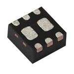
| 描述 | MOSFET N-CH 20V 6A SC-75-6 |
| 产品分类 | FET - 单 |
| FET功能 | 逻辑电平门 |
| FET类型 | MOSFET N 通道,金属氧化物 |
| 品牌 | Vishay Siliconix |
| 数据手册 | |
| 产品图片 |
|
| 产品型号 | SIB406EDK-T1-GE3 |
| rohs | 无铅 / 符合限制有害物质指令(RoHS)规范要求 |
| 产品系列 | TrenchFET® |
| 不同Id时的Vgs(th)(最大值) | 1.4V @ 250µA |
| 不同Vds时的输入电容(Ciss) | 350pF @ 10V |
| 不同Vgs时的栅极电荷(Qg) | 12nC @ 10V |
| 不同 Id、Vgs时的 RdsOn(最大值) | 46 毫欧 @ 3.9A,4.5V |
| 供应商器件封装 | PowerPAK® SC-75-6L 单 |
| 其它名称 | SIB406EDK-T1-GE3CT |
| 功率-最大值 | 10W |
| 包装 | 剪切带 (CT) |
| 安装类型 | 表面贴装 |
| 封装/外壳 | PowerPAK® SC-75-6L |
| 标准包装 | 1 |
| 漏源极电压(Vdss) | 20V |
| 电流-连续漏极(Id)(25°C时) | 6A (Tc) |


PDF Datasheet 数据手册内容提取
SiB406EDK www.vishay.com Vishay Siliconix N-Channel 20 V (D-S) MOSFET FEATURES PowerPAK® SC-75-6L Single D • TrenchFET® power MOSFET D 6 S 5 • New thermally enhanced PowerPAK® SC-75 4 package - Small footprint area - Low on-resistance 1.6 S7 2 D1 • Typical ESD protection 560 V mm 1 1.6 mm G3 D • pMleaatesreia sl eec awtewgwo.rvizisahtiaoyn.c: ofmor/ dodce?fi9n9it9io1n2s of complianc e Top View Bottom View Marking code: AD APPLICATIONS D PRODUCT SUMMARY • Load switch for portabl e applications V (V) 20 DS • High frequency DC/D C RDS(on) max. () at VGS = 4.5 V 0.046 G converter RDS(on) max. () at VGS = 2.5 V 0.063 Q typ. (nC) 3.5 g I (A) a 6 D Configuration Single N-Channel MOSFET S ORDERING INFORMATION Package SC-75 Lead (Pb)-free and halogen-free SiB406EDK-T1-GE3 ABSOLUTE MAXIMUM RATINGS (T = 25 °C, unless otherwise noted) A PARAMETER SYMBOL LIMIT UNIT Drain-source voltage V 20 DS V Gate-source voltage V ± 12 GS T = 25 °C 6 a C T = 70 °C 6 a Continuous drain current (T = 150 °C) C I J T = 25 °C D 5.1 b, c A T = 70 °C 4.1 b, c A A Pulsed drain current I 15 DM T = 25 °C 6 a Continuous source-drain diode current C I T = 25 °C S 1.6 b, c A T = 25 °C 10 C T = 70 °C 6.4 Maximum power dissipation C P W T = 25 °C D 1.95 b, c A T = 70 °C 1.25 b, c A Operating junction and storage temperature range T , T -55 to +150 J stg °C Soldering recommendations (peak temperature) d, e 260 THERMAL RESISTANCE RATINGS PARAMETER SYMBOL TYPICAL MAXIMUM UNIT Maximum junction-to-ambient b, f t 5 s RthJA 51 64 °C/W Maximum junction-to-case (drain) Steady state R 10 12.5 thJC Notes a. Package limited b. Surface mounted on 1" x 1" FR4 board c. t = 5 s d. See solder profile (www.vishay.com/doc?73257). The PowerPAK SC-75 is a leadless package. The end of the lead terminal is exposed copper (not plated) as a result of the singulation process in manufacturing. A solder fillet at the exposed copper tip cannot be guarantee d and is not required to ensure adequate bottom side solder interconnection e. Rework conditions: manual soldering with a soldering iron is not recommended for leadless components f. Maximum under steady state conditions is 100 °C/W S-83095-Rev. A, 29-Dec-08 1 Document Number: 69088 For technical questions, contact: pmostechsupport@vishay.com THIS DOCUMENT IS SUBJECT TO CHANGE WITHOUT NOTICE. THE PRODUCTS DESCRIBED HEREIN AND THIS DOCUMENT ARE SUBJECT TO SPECIFIC DISCLAIMERS, SET FORTH AT www.vishay.com/doc?91000
SiB406EDK www.vishay.com Vishay Siliconix SPECIFICATIONS (T = 25 °C, unless otherwise noted) J PARAMETER SYMBOL TEST CONDITIONS MIN. TYP. MAX. UNIT Static Drain-source breakdown voltage V V = 0 V, I = 250 μA 20 - - V DS GS D VDS temperature coefficient VDS/TJ - 23 - I = 250 μA mV/°C D VGS(th) temperature coefficient VGS(th)/TJ - -3.3 - Gate-source threshold voltage V V = V , I = 250 μA 0.6 - 1.4 V GS(th) DS GS D Gate-source leakage I V = 0 V, V = ± 12 V - - ± 8 GSS DS GS V = 20 V, V = 0 V - - -1 μA DS GS Zero gate voltage drain current I DSS V = 20 V, V = 0 V, T = 55 °C - - -10 DS GS J On-state drain current a ID(on) VDS 5 V, VGS = 4.5 V 10 - - A V = 4.5 V, I = 3.9 A - 0.037 0.046 Drain-source on-state resistance a RDS(on) GS D V = 2.5 V, I = 3.3 A - 0.051 0.063 GS D Forward transconductance a g V = 10 V, I = 3.9 A - 14 - S fs DS D Dynamic b Input capacitance C - 350 - iss Output capacitance Coss VDS = 10 V, VGS = 0 V, f = 1 MHz - 63 - pF Reverse transfer capacitance C - 37 - rss VDS = 10 V, VGS = 10 V, ID = 5.1 A - 7.5 12 Total gate charge Q g - 3.5 5.5 nC Gate-source charge Qgs VDS = 10 V, VGS = 4.5 V, ID = 5.1 A - 0.95 - Gate-drain charge Q - 0.75 - gd Gate resistance Rg f = 1 MHz - 3.5 - Turn-on delay time t - 10 15 d(on) Rise time tr VDD = 10 V, RL = 2.4 - 12 20 Turn-off delay time td(off) ID 4.1 A, VGEN = 4.5 V, Rg = 1 - 18 30 Fall time t - 12 20 f ns Turn-on delay time t - 5 10 d(on) Rise time tr VDD = 10 V, RL = 2.4 - 12 20 Turn-off delay time td(off) ID 4.1 A, VGEN = 10 V, Rg = 1 - 15 25 Fall time t - 10 15 f Drain-Source Body Diode Characteristics Continuous source-drain diode current I T = 25 °C - - 6 S C A Pulse diode forward current I - - 15 SM Body diode voltage VSD IS = 4.1 A, VGS = 0 V - 0.8 1.2 V Body diode reverse recovery time t - 15 30 ns rr Body diode reverse recovery charge Qrr IF = 4.1 A, di/dt = 100 A/μs, - 8 20 nC Reverse recovery fall time ta TJ = 25 °C - 8 - ns Reverse recovery rise time t - 7 - b Notes a. Pulse test; pulse width 300 μs, duty cycle 2 % b. Guaranteed by design, not subject to production testing Stresses beyond those listed under “Absolute Maximum Ratings” may cause permanent damage to the device. These are stress ratings only, and functional operation of the device at these or any other conditions beyond those indicated in the operational sections of the specifications is not implied. Exposure to absolute maximum rating conditions for extended periods may affect device reliability. S-83095-Rev. A, 29-Dec-08 2 Document Number: 69088 For technical questions, contact: pmostechsupport@vishay.com THIS DOCUMENT IS SUBJECT TO CHANGE WITHOUT NOTICE. THE PRODUCTS DESCRIBED HEREIN AND THIS DOCUMENT ARE SUBJECT TO SPECIFIC DISCLAIMERS, SET FORTH AT www.vishay.com/doc?91000
SiB406EDK www.vishay.com Vishay Siliconix TYPICAL CHARACTERISTICS (25 °C, unless otherwise noted) 4 10-2 10-3 mA) 3 A) 10-4 - Gate Current (IGSS 12 IGSS at 25 °C - Gate Current (IGSS 11110000----8765 TJ = 150 °C TJ = 25 °C 10-9 0 10-10 0 3 6 9 12 15 18 0 3 6 9 12 15 18 VGS-Gate-to-SourceVoltage(V) VGS-Gate-to-SourceVoltage(V) Gate Current vs. Gate-Source Voltage Gate Current vs. Gate-Source Voltage 15 5 VGS=5Vthru3V VGS=2.5V 12 4 A) A) TC=-55 °C ( ( Current 9 Current 3 Drain 6 Drain 2 - ID VGS=2V - ID TC=25 °C 3 1 TC=125 °C VGS=1.5V 0 0 0.0 0.5 1.0 1.5 2.0 2.5 3.0 0.0 0.5 1.0 1.5 2.0 VDS-Drain-to-SourceVoltage(V) VGS-Gate-to-SourceVoltage(V) Output Characteristics Transfer Characteristics 0.12 500 Ω() 0.09 400 Ciss ce F) - On-ResistanS(on) 0.06 VGS=2.5V VGS=4.5V C - Capacitance(p 230000 RD 0.03 Coss 100 Crss 0.00 0 0 3 6 9 12 15 0 2 4 6 8 10 12 14 16 18 20 ID-DrainCurrent(A) VDS-Drain-to-SourceVoltage(V) On-Resistance vs. Drain Current and Gate Voltage Capacitance S-83095-Rev. A, 29-Dec-08 3 Document Number: 69088 For technical questions, contact: pmostechsupport@vishay.com THIS DOCUMENT IS SUBJECT TO CHANGE WITHOUT NOTICE. THE PRODUCTS DESCRIBED HEREIN AND THIS DOCUMENT ARE SUBJECT TO SPECIFIC DISCLAIMERS, SET FORTH AT www.vishay.com/doc?91000
SiB406EDK www.vishay.com Vishay Siliconix TYPICAL CHARACTERISTICS (25 °C, unless otherwise noted) 10 1.7 ID=5.1A ID=3.9A (V) 8 1.5 e SourceVoltag 6 VDS=10V VDS=16V n-Resistance malized) 11..13 VGS=4.5V,2.5V Gate-to- 4 - OS(on)(Nor 0.9 - S RD VG 2 0.7 0 0.5 0 2 4 6 8 - 50 - 25 0 25 50 75 100 125 150 Qg-TotalGateCharge(nC) TJ-JunctionTemperature(°C) Gate Charge On-Resistance vs. Junction Temperature 100 0.20 ID=2A Ω) 0.16 nt(A) 10 ance( Curre Resist 0.12 - SourceIS 1 TJ=150 °C TJ=25 °C - On-RDS(on) 0.08 TJ=125 °C 0.04 TJ=25 °C 0.1 0.00 0.0 0.2 0.4 0.6 0.8 1.0 1.2 1.4 0 1 2 3 4 5 VSD-Source-to-DrainVoltage(V) VGS-Gate-to-SourceVoltage(V) Source-Drain Diode Forward Voltage On-Resistance vs. Gate-to-Source Voltage 1.3 30 1.2 25 1.1 ID=250 µA 20 V) 1.0 W) (GS(th) 0.9 ower ( 15 V P 10 0.8 0.7 5 0.6 0 - 50 - 25 0 25 50 75 100 125 150 0.001 0.01 0.1 1 10 100 1000 TJ-Temperature(°C) Pulse (s) Threshold Voltage Single Pulse Power (Junction-to-Ambient) S-83095-Rev. A, 29-Dec-08 4 Document Number: 69088 For technical questions, contact: pmostechsupport@vishay.com THIS DOCUMENT IS SUBJECT TO CHANGE WITHOUT NOTICE. THE PRODUCTS DESCRIBED HEREIN AND THIS DOCUMENT ARE SUBJECT TO SPECIFIC DISCLAIMERS, SET FORTH AT www.vishay.com/doc?91000
SiB406EDK www.vishay.com Vishay Siliconix TYPICAL CHARACTERISTICS (25 °C, unless otherwise noted) 100 LimitedbyRDS(on)* 10 A) 100µs ( nt e urr 1ms C 1 n ai 10ms Dr -D 100ms I 0.1 1s,10s TA=25 °C DC SinglePulse BVDSSLimited 0.01 0.1 1 10 100 VDS-Drain-to-SourceVoltage(V) *VGS>minimumVGSatwhichRDS(on)isspecified Safe Operating Area, Junction-to-Ambient 15 12 12 Current(A) 9 sipation (W) 69 Drain 6 PackageLimited er Dis w -D Po I 3 3 0 0 0 25 50 75 100 125 150 25 50 75 100 125 150 TC-CaseTemperature(°C) TC - Case Temperature (°C) Current Derating a Power Derating Note a. The power dissipation P is based on T max. = 150 °C, using junction-to-case thermal resistance, and is more useful in settling the upper D J dissipation limit for cases where additional heatsinking is used. It is used to determine the current rating, when this rating falls below the package limit S-83095-Rev. A, 29-Dec-08 5 Document Number: 69088 For technical questions, contact: pmostechsupport@vishay.com THIS DOCUMENT IS SUBJECT TO CHANGE WITHOUT NOTICE. THE PRODUCTS DESCRIBED HEREIN AND THIS DOCUMENT ARE SUBJECT TO SPECIFIC DISCLAIMERS, SET FORTH AT www.vishay.com/doc?91000
SiB406EDK www.vishay.com Vishay Siliconix TYPICAL CHARACTERISTICS (25 °C, unless otherwise noted) 1 DutyCycle=0.5 nt e Transiance 0.2 ctivemped 0.1 Notes: edEffeermalI 0.1 0.05 PDM zh maliT 0.02 t1 Nor 1.DutyCyclet,2D= tt12 2.PerUnitBase=RthJA=100 °C/W 3.TJM-TA=PDMZthJA(t) SinglePulse 4.SurfaceMounted 0.01 10-4 10-3 10-2 10-1 1 10 100 1000 Square Wave Pulse Duration (s) Normalized Thermal Transient Impedance, Junction-to-Ambient 1 DutyCycle=0.5 nt e 0.2 edEffectiveTransiermalImpedance 0.1 S0.in1gle0P.0u2lse0.05 alizTh m or N 0.01 10-4 10-3 10-2 10-1 SquareWavePulseDuration(s) Normalized Thermal Transient Impedance, Junction-to-Case Vishay Siliconix maintains worldwide manufacturing capability. Products may be manufactured at one of several qualified locations. Reliability data for Silico n Technology and Package Reliability represent a composite of all qualified locations. For related documents such as package / tape drawings, part marking, and reliability data, see www.vishay.com/ppg?69088. S-83095-Rev. A, 29-Dec-08 6 Document Number: 69088 For technical questions, contact: pmostechsupport@vishay.com THIS DOCUMENT IS SUBJECT TO CHANGE WITHOUT NOTICE. THE PRODUCTS DESCRIBED HEREIN AND THIS DOCUMENT ARE SUBJECT TO SPECIFIC DISCLAIMERS, SET FORTH AT www.vishay.com/doc?91000
Package Information Vishay Siliconix PowerPAK® SC75-6L e b e b PIN1 PIN2 PIN3 PIN1 PIN2 PIN3 L L D2 K4 K 2 1 E 1 1 E D1 3 E D1 D1 E E K K PIN6 PIN5 PIN4 PIN6 PIN5 PIN4 K3 K1 KK22 K2 K1 K2 BACKSIDE VIEW OF SINGLE BACKSIDE VIEW OF DUAL D A Notes: 1. All dimensions are in millimeters 2. Package outline exclusive of mold flash and metal burr 3. Package outline inclusive of plating E A1 C Z z DETAIL Z SINGLE PAD DUAL PAD DIM MILLIMETERS INCHES MILLIMETERS INCHES Min Nom Max Min Nom Max Min Nom Max Min Nom Max A 0.675 0.75 0.80 0.027 0.030 0.032 0.675 0.75 0.80 0.027 0.030 0.032 A1 0 - 0.05 0 - 0.002 0 - 0.05 0 - 0.002 b 0.18 0.25 0.33 0.007 0.010 0.013 0.18 0.25 0.33 0.007 0.010 0.013 C 0.15 0.20 0.25 0.006 0.008 0.010 0.15 0.20 0.25 0.006 0.008 0.010 D 1.53 1.60 1.70 0.060 0.063 0.067 1.53 1.60 1.70 0.060 0.063 0.067 D1 0.57 0.67 0.77 0.022 0.026 0.030 0.34 0.44 0.54 0.013 0.017 0.021 D2 0.10 0.20 0.30 0.004 0.008 0.012 E 1.53 1.60 1.70 0.060 0.063 0.067 1.53 1.60 1.70 0.060 0.063 0.067 E1 1.00 1.10 1.20 0.039 0.043 0.047 0.51 0.61 0.71 0.020 0.024 0.028 E2 0.20 0.25 0.30 0.008 0.010 0.012 E3 0.32 0.37 0.42 0.013 0.015 0.017 e 0.50 BSC 0.020 BSC 0.50 BSC 0.020 BSC K 0.180 TYP 0.007 TYP 0.245 TYP 0.010 TYP K1 0.275 TYP 0.011 TYP 0.320 TYP 0.013 TYP K2 0.200 TYP 0.008 TYP 0.200 BSC 0.008 TYP K3 0.255 TYP 0.010 TYP K4 0.300 TYP 0.012 TYP L 0.15 0.25 0.35 0.006 0.010 0.014 0.15 0.25 0.35 0.006 0.010 0.014 T 0.03 0.08 0.13 0.001 0.003 0.005 ECN: C-07431 − Rev. C, 06-Aug-07 DWG: 5935 Document Number: 73000 www.vishay.com 06-Aug-07 1
Application Note 826 Vishay Siliconix RECOMMENDED PAD LAYOUT FOR PowerPAK® SC75-6L Single 1.250 (0.049) 0.250 (0.01) 0.250 (0.01) 0.500 (0.02) 0.400 (0.016) 0.300 (0.012) 0.180 (0.007) 0.370 (0.015) (0.043) 0.620 (0.024) 1.700 (0.067) 1.100 2.000 (0.079) 0.200 (0.008) 0.300 (0.012) 0.300 (0.012) 1 0.545 (0.021) 0.250 (0.01) 0.670 (0.026) 2.000 (0.079) Dimensions in mm/(Inches) Return to Index A P P L I C A T I O N N O T E Document Number: 70488 www.vishay.com Revision: 21-Jan-08 13
Legal Disclaimer Notice www.vishay.com Vishay Disclaimer ALL PRODUCT, PRODUCT SPECIFICATIONS AND DATA ARE SUBJECT TO CHANGE WITHOUT NOTICE TO IMPROV E RELIABILITY, FUNCTION OR DESIGN OR OTHERWISE. Vishay Intertechnology, Inc., its affiliates, agents, and employees, and all persons acting on its or their behalf (collectively, “Vishay”), disclaim any and all liability for any errors, inaccuracies or incompleteness contained in any datasheet or in any other disclosure relating to any product. Vishay makes no warranty, representation or guarantee regarding the suitability of the products for any particular purpose o r the continuing production of any product. To the maximum extent permitted by applicable law, Vishay disclaims (i) any and all liability arising out of the application or use of any product, (ii) any and all liability, including without limitation special, consequential or incidental damages, and (iii) any and all implied warranties, including warranties of fitness for particular purpose, non-infringement and merchantability. Statements regarding the suitability of products for certain types of applications are based on Vishay’s knowledge of typical requirements that are often placed on Vishay products in generic applications. Such statements are not binding statements about the suitability of products for a particular application. It is the customer’s responsibility to validate that a particular product with the properties described in the product specification is suitable for use in a particular application. Parameters provided in datasheets and / or specifications may vary in different applications and performance may vary over time. All operating parameters, including typical parameters, must be validated for each customer application by the customer’s technical experts. Product specifications do not expand or otherwise modify Vishay’s terms and conditions of purchase, including but not limited to the warranty expressed therein. Except as expressly indicated in writing, Vishay products are not designed for use in medical, life-saving, or life-sustainin g applications or for any other application in which the failure of the Vishay product could result in personal injury or death. Customers using or selling Vishay products not expressly indicated for use in such applications do so at their own risk . Please contact authorized Vishay personnel to obtain written terms and conditions regarding products designed for such applications. No license, express or implied, by estoppel or otherwise, to any intellectual property rights is granted by this documen t or by any conduct of Vishay. Product names and markings noted herein may be trademarks of their respective owners. © 2019 VISHAY INTERTECHNOLOGY, INC. ALL RIGHTS RESERVED Revision: 01-Jan-2019 1 Document Number: 91000
Mouser Electronics Authorized Distributor Click to View Pricing, Inventory, Delivery & Lifecycle Information: V ishay: SIB406EDK-T1-GE3