ICGOO在线商城 > SI-3033LSA-TL

 Datasheet下载
- 型号: SI-3033LSA-TL
- 制造商: Sanken
- 库位|库存: xxxx|xxxx
- 要求:
| 数量阶梯 | 香港交货 | 国内含税 |
| +xxxx | $xxxx | ¥xxxx |
查看当月历史价格
查看今年历史价格
SI-3033LSA-TL产品简介:
ICGOO电子元器件商城为您提供SI-3033LSA-TL由Sanken设计生产,在icgoo商城现货销售,并且可以通过原厂、代理商等渠道进行代购。 提供SI-3033LSA-TL价格参考以及SankenSI-3033LSA-TL封装/规格参数等产品信息。 你可以下载SI-3033LSA-TL参考资料、Datasheet数据手册功能说明书, 资料中有SI-3033LSA-TL详细功能的应用电路图电压和使用方法及教程。
| 参数 | 数值 |
| 产品目录 | 集成电路 (IC) |
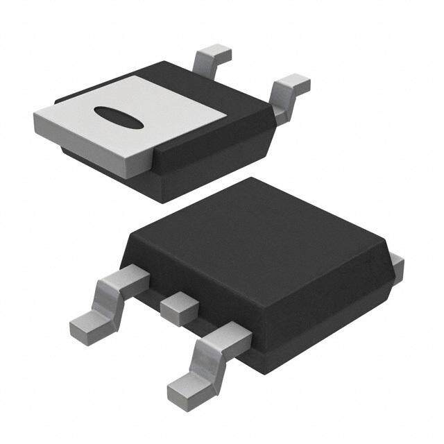
| 描述 | IC REG LDO 3.3V 1A 8SOP |
| 产品分类 | |
| 品牌 | Sanken |
| 数据手册 | |
| 产品图片 |
|
| 产品型号 | SI-3033LSA-TL |
| rohs | 无铅 / 符合限制有害物质指令(RoHS)规范要求 |
| 产品系列 | - |
| 供应商器件封装 | 8-SOP |
| 其它名称 | SI-3033LSA-TLCT |
| 包装 | 剪切带 (CT) |
| 安装类型 | 表面贴装 |
| 封装/外壳 | 8-SOIC(0.173",4.40mm 宽) |
| 工作温度 | -30°C ~ 85°C |
| 标准包装 | 1 |
| 电压-跌落(典型值) | - |
| 电压-输入 | 高达 5.2V |
| 电压-输出 | 3.3V |
| 电流-输出 | 1A |
| 电流-限制(最小值) | - |
| 稳压器拓扑 | 正,固定式 |
| 稳压器数 | 1 |


.jpg)


- 商务部:美国ITC正式对集成电路等产品启动337调查
- 曝三星4nm工艺存在良率问题 高通将骁龙8 Gen1或转产台积电
- 太阳诱电将投资9.5亿元在常州建新厂生产MLCC 预计2023年完工
- 英特尔发布欧洲新工厂建设计划 深化IDM 2.0 战略
- 台积电先进制程称霸业界 有大客户加持明年业绩稳了
- 达到5530亿美元!SIA预计今年全球半导体销售额将创下新高
- 英特尔拟将自动驾驶子公司Mobileye上市 估值或超500亿美元
- 三星加码芯片和SET,合并消费电子和移动部门,撤换高东真等 CEO
- 三星电子宣布重大人事变动 还合并消费电子和移动部门
- 海关总署:前11个月进口集成电路产品价值2.52万亿元 增长14.8%

_renders/CS4265-CNZR.jpg)

PDF Datasheet 数据手册内容提取
1-1-4 Linear Regulator ICs SI-3000LSA Series Surface-Mount, Low Current Consumption, Low Dropout Voltage ■ Features ■ Absolute Maximum Ratings (Ta=25°C) •Compact surface-mount package (SOP8) Parameter Symbol Ratings Unit •Output current: 1 A DC Input Voltage VIN 16 V Output control terminal voltage VC VIN V •Low circuit current at output OFF: Iq(OFF) ≤ 1 DC Output Current IO 1 A µA (VC = 0 V) PD1*1 1.16 W Power Dissipation •Low dropout voltage: VDIF≤0.8 V (at IO = 1 A) PD2*2 1.1 W VDIF ≤1.2 V (IO = 1 A) for SI-3018LSA Junction Temperature Tj*3 –30 to +150 °C Operating Ambient Temperature Top –30 to +150 °C •4 types of output voltages (1.8 V, 2.5 V, 3.3 V, Storage Temperature Tstg –30 to +150 °C 5.0 V) available Thermal Resistance (Junction to Lead (pin 8)) θj-L 36 °C/W •Output ON/OFF control terminal voltage Thermal Resistance (Junction to Ambient Air) θj-a*2 100 °C/W compatible with LS-TTL *1:When mounted on glass-epoxy board 56.5 × 56.5 mm (copper laminate area 100%). •Built-in foldback-type-overcurrent and thermal *2:When mounted on glass-epoxy board 40 × 40 mm (copper laminate area 100%). *3:Thermal protection circuits may be activated if the junction temperature exceeds 135°C. protection circuits ■ Applications •Auxiliary power supplies for PC •Battery-driven electronic equipment ■ Recommended Operating Conditions Ratings Parameter Symbol Unit SI-3018LSA SI-3025LSA SI-3033LSA SI-3050LSA DC Input Voltage Range VIN 3.1 to 3.5*1 *2 to 3.5*1 *2 to 5.2*1 *2 to 8.0 V DC Output Current Range IO 0 to 1 A Operating Junction Temperature Tjop –20 to +125 °C Operating Ambient Temperature Taop –30 to +85 °C *1:VIN (max) and IO (max) are restricted by the relation PD = (VIN – VO) × IO. Please calculate these values referring to the reference data on page 71. *2:Refer to the Dropout Voltage parameter. ■ Electrical Characteristics (Ta=25°C, VC=2V, unless otherwise specified) Ratings Parameter Symbol SI-3018LSA SI-3025LSA SI-3033LSA SI-3050LSA Unit min. typ. max. min. typ. max. min. typ. max. min. typ. max. VO 1.764 1.800 1.836 2.450 2.500 2.550 3.234 3.300 3.366 4.90 5.00 5.10 Output Voltage V Conditions VIN=3.3V, IO=0.5A VIN=3.3V, IO=0.5A VIN=5V, IO=0.5A VIN=6V, IO=0.5A VDIF – 0.4 0.4 0.4 Conditions – IO≤0.5A IO≤0.5A IO≤0.5A Dropout Voltage V 0.6 1.2 0.8 0.8 0.8 Conditions IO≤1A ∆VLINE 2 10 2 10 3 10 3 15 Line Regulation mV Conditions VIN=3.1 to 3.5V, IO=0.3A VIN=3.1 to 3.5V, IO=0.3A VIN=4.5 to 5.5V, IO=0.3A VIN=6 to 7V, IO=0.3A ∆VOLOAD 10 20 10 20 10 20 10 30 Load Regulation mV Conditions VIN=3.3V, IO=0 to 1A VIN=3.3V, IO=0 to 1A VIN=5V, IO=0 to 1A VIN=6V, IO=0 to 1A Temperature Coefficient of ∆VO/∆Ta ±0.3 ±0.3 ±0.3 ±0.5 Output Voltage Conditions VIN=3.3V, IO=5mA, Tj=0 to 100°C VIN=3.3V, IO=5mA, Tj=0 to 100°C VIN=5V, IO=5mA, Tj=0 to 100°C VIN=6V, IO=5mA, Tj=0 to 100°C mV/°C RREJ 60 57 55 55 Ripple Rejection dB Conditions VIN=3.3V, f=100 to 120HZ VIN=3.3V, f=100 to 120HZ VIN=5V, f=100 to 120HZ VIN=6V, f=100 to 120HZ Iq 1.7 2.5 1.7 2.5 1.7 2.5 1.7 2.5 Quiescent Circuit Current mA Conditions VIN=3.3V, IO=0A VIN=3.3V, IO=0A VIN=5V, IO=0A VIN=6V, IO=0A Iq(OFF) 1 1 1 1 Circuit Current at Output OFF µA Conditions VIN=3.3V, IO=0A, VC=0V VIN=3.3V, IO=0A, VC=0V VIN=5V, IO=0A, VC=0V VIN=6V, IO=0A, VC=0V Overcurrent Protection IS1 1.2 1.2 1.2 1.2 Starting Current*1,3 Conditions VIN=3.3V VIN=3.3V VIN=5V VIN=6V A Control Voltage (Output ON)*2 VC, IH 2.0 2.0 2.0 2.0 V Control Voltage (Output OFF)*2 VC, IL 0.8 0.8 0.8 0.8 VC IC, IH 40 80 40 80 40 80 40 80 Control Current (Output ON) µA Terminal Conditions VC=2V IC, IL 0 –5 0 –5 0 –5 0 –5 Control Current (Output OFF) µA Conditions VC=0V *1:Is1 is specified at the 5% drop point of output voltage VO on the condition that VIN = 3.3 V (5 V for SI-3033LSA), and IO = 0.5 A. *2:Output is OFF when the output control terminal VC is open. Each input level is equivalent to LS-TTL level. Therefore, the device can be driven directly by LS-TTLs. *3:These products cannot be used in the following applications. Because these applications require a certain current at start-up and so the built-in foldback-type overcurrent protection may cause errors during start-up stage. (1) Constant current load (2) Positive and negative power supply (3) Series-connected power supply (4) VO adjustment by raising ground voltage 70 ICs
SI-3000LSA Series ■ External Dimensions (SOP8) (Unit : mm) 5.1±0.4 1.27 0.4±0.1 0.15+–00..105 Pin Assignment 8 7 6 5 0.1±0.5 qw VNICN (Leave open) e VIN 0.2±4.4 0.3±6.2 rt VGCND y GND 1 2 3 4 u VO 0.995max. 1.27 0 to 10° i VO 0.1±1.50.15±1.55 PFllaamstmic aMboililtdy :P UaLck9a4gVe-0 Type 0.4±0.1 00.1.120M 0.05±0.05 Product Mass: Approx. 0.1g ■ Block Diagram VIN 1 8 VO NC 2 7 VO + – VIN 3 TSD 6 GND VC 4 5 GND ■ Typical Connection Diagram VIN VO 1 8 CO: Output capacitor (22 µF or larger) + CIN 234 765 + oad CIN:ITnhpius tc caappaaccitiotorr i s(1 r0e qµuFi)red in the case of an inductive input line or long VIN L wiring. GND CO Tantalum capacitors are recommended for CIN and CO, particularly at VC low temperatures. * Leave pin 2 open. ■ Reference Data PCB Copper Laminate Area vs. Junction to Allowable Output Current Ambient Air Thermal Resistance (vs. VIN-VOUT Voltage Difference) VIN-IO max 150 1.2 140 P16C0Bm (mgl a(4ss0-×e4p0o)x my,m 40×40mm) 1.0 Tj = 120°C (20% derating of 150°C) The inner frame stage, on which the PTr is mounted, 130 is directly connected to the VOUT pin. 0.8 θ°(C/W)j-a 111210000 Imax) (A)out ( 00..64 θj-a=100°C/WTa=25°C Tararhdoeiuarnetidofo ntr.hee, eVnOlUaTr gpiinng i st hreea clloyp epfeferc ltaivmei nfoart ea ahreeaat 90 80 0.2 Ta=85°C 70 0 100 1000 5000 1 2 3 4 Copper Laminate Area (mm2) VIN-VOUT Voltage Difference (V) ICs 71