ICGOO在线商城 > 集成电路(IC) > PMIC - 稳压器 - DC DC 切换控制器 > SG2525AP

 Datasheet下载
- 型号: SG2525AP
- 制造商: STMicroelectronics
- 库位|库存: xxxx|xxxx
- 要求:
| 数量阶梯 | 香港交货 | 国内含税 |
| +xxxx | $xxxx | ¥xxxx |
查看当月历史价格
查看今年历史价格
SG2525AP产品简介:
ICGOO电子元器件商城为您提供SG2525AP由STMicroelectronics设计生产,在icgoo商城现货销售,并且可以通过原厂、代理商等渠道进行代购。 SG2525AP价格参考。STMicroelectronicsSG2525AP封装/规格:PMIC - 稳压器 - DC DC 切换控制器, 降压,推挽 稳压器 正 输出 降压,升压/降压 DC-DC 控制器 IC 16-SO。您可以下载SG2525AP参考资料、Datasheet数据手册功能说明书,资料中有SG2525AP 详细功能的应用电路图电压和使用方法及教程。
SG2525AP是由STMicroelectronics(意法半导体)制造的一款PMIC(电源管理集成电路),具体分类为DC-DC切换控制器。该器件广泛应用于需要高效、可靠电源转换的场合,尤其适合那些要求高精度电压调节和较大电流输出的应用。

 应用场景

1. 工业控制系统:
   SG2525AP适用于工业自动化设备中的电源管理系统。它能够为PLC(可编程逻辑控制器)、传感器、执行器等提供稳定可靠的电源。其高效的DC-DC转换特性可以确保在复杂电磁环境下依然保持性能稳定,减少电力损耗,延长设备使用寿命。

2. 通信基础设施:
   在基站、路由器、交换机等通信设备中,SG2525AP用于将输入电压转换为所需的稳定输出电压。它支持宽范围输入电压,能够在不同供电条件下正常工作,保证通信设备的稳定运行,特别是在远程或野外环境中。

3. 消费电子设备:
   例如笔记本电脑、平板电脑和智能电视等消费电子产品中,SG2525AP可以作为电源管理芯片,提供高效的电源转换。其低功耗特性和紧凑的封装设计使得它可以轻松集成到小型化、便携式的设备中,同时确保设备在长时间使用时不会过热。

4. 汽车电子系统:
   汽车内的各种电子模块,如车载信息娱乐系统、导航系统、驾驶辅助系统等,都需要稳定的电源供应。SG2525AP可以承受较大的电压波动和温度变化,确保这些系统在各种工况下都能正常工作,提高行车安全性和舒适性。

5. 医疗设备:
   在医疗仪器中,如监护仪、超声设备等,SG2525AP可以提供精确的电压调节,确保设备的测量精度和可靠性。其低噪声特性有助于减少对敏感信号的干扰,提升诊断结果的准确性。

总之,SG2525AP凭借其高性能、高可靠性和灵活性,广泛应用于各类需要高效电源管理的领域,为现代电子设备提供了坚实的电源保障。
| 参数 | 数值 |
| 产品目录 | 集成电路 (IC)半导体 |
| Cuk | 无 |
| 描述 | IC REG CTRLR PWM VM 16-SOIC开关控制器 Voltage Mode w/Sync |
| 产品分类 | |
| 品牌 | STMicroelectronics |
| 产品手册 | |
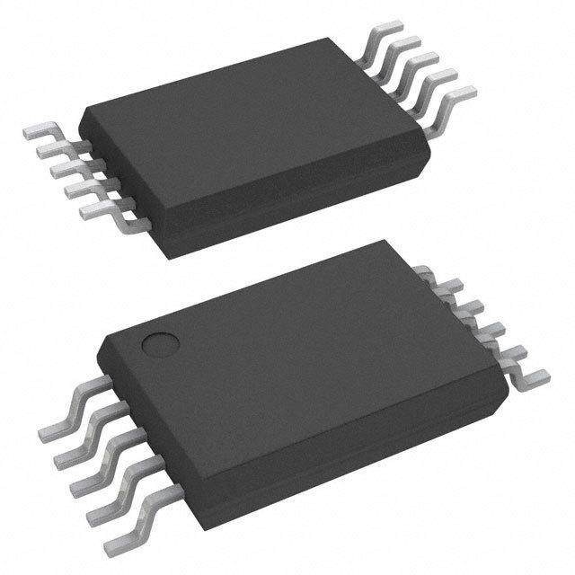
| 产品图片 |
|
| rohs | 符合RoHS无铅 / 符合限制有害物质指令(RoHS)规范要求 |
| 产品系列 | 电源管理 IC,开关控制器 ,STMicroelectronics SG2525AP- |
| 数据手册 | |
| 产品型号 | SG2525AP |
| PWM类型 | 电压模式 |
| 产品 | Voltage Controllers |
| 产品培训模块 | http://www.digikey.cn/PTM/IndividualPTM.page?site=cn&lang=zhs&ptm=26258 |
| 产品目录页面 | |
| 产品种类 | 开关控制器 |
| 倍增器 | 无 |
| 其它名称 | 497-6726-5 |
| 其它有关文件 | http://www.st.com/web/catalog/sense_power/FM142/CL1454/SC352/PF75183?referrer=70071840 |
| 分频器 | 无 |
| 包装 | 管件 |
| 升压 | 无 |
| 占空比 | 49% |
| 占空比-最大 | 49 % |
| 反向 | 无 |
| 反激式 | 无 |
| 商标 | STMicroelectronics |
| 安装风格 | SMD/SMT |
| 封装 | Tube |
| 封装/外壳 | 16-SOIC(0.154",3.90mm 宽) |
| 封装/箱体 | SO-16 |
| 工作温度 | -25°C ~ 85°C |
| 工厂包装数量 | 50 |
| 开关频率 | 500 kHz |
| 最大工作温度 | + 85 C |
| 最小工作温度 | - 25 C |
| 标准包装 | 50 |
| 电压-电源 | 8 V ~ 35 V |
| 类型 | PWM Controllers |
| 系列 | SG2525 |
| 输出数 | 2 |
| 输出电压 | 5.15 V |
| 输出端数量 | 2 Output |
| 降压 | 无 |
| 隔离式 | 无 |
| 频率-最大值 | 500kHz |


- 商务部:美国ITC正式对集成电路等产品启动337调查
- 曝三星4nm工艺存在良率问题 高通将骁龙8 Gen1或转产台积电
- 太阳诱电将投资9.5亿元在常州建新厂生产MLCC 预计2023年完工
- 英特尔发布欧洲新工厂建设计划 深化IDM 2.0 战略
- 台积电先进制程称霸业界 有大客户加持明年业绩稳了
- 达到5530亿美元!SIA预计今年全球半导体销售额将创下新高
- 英特尔拟将自动驾驶子公司Mobileye上市 估值或超500亿美元
- 三星加码芯片和SET,合并消费电子和移动部门,撤换高东真等 CEO
- 三星电子宣布重大人事变动 还合并消费电子和移动部门
- 海关总署:前11个月进口集成电路产品价值2.52万亿元 增长14.8%


PDF Datasheet 数据手册内容提取
SG2525A SG3525A ® REGULATING PULSE WIDTH MODULATORS . . .8 TO 35 V OPERATION .5.1 V REFERENCE TRIMMED TO – 1 % .100 Hz TO 500 KHz OSCILLATOR RANGE .SEPARATE OSCILLATOR SYNC TERMINAL .ADJUSTABLE DEADTIME CONTROL .INTERNAL SOFT-START PULSE-BY-PULSE SHUTDOWN .INPUT UNDERVOLTAGE LOCKOUT WITH HYSTERESIS DIP16 16(Narrow) .LATCHING PWM TO PREVENT MULTIPLE PULSES DUAL SOURCE/SINK OUTPUT DRIVERS DESCRIPTION The SG3525A series of pulse width modulator inte- turn off through the PWM latch with pulsed shut- grated circuits are designed to offer improved per- down, as well as soft-start recycle with longer shut- formance and lowered external parts count when down commands. These functions are also control- used in designing all types of switching power sup- led by an undervoltage lockout which keeps the out- plies. The on-chip + 5.1 V reference is trimmed to – puts off and the soft-start capacitor discharged for 1 % and the input common-mode range of the error sub-normal input voltages. This lockout circuitry in- amplifier includes the reference voltage eliminating cludes approximately 500 mV of hysteresis for jitter- external resistors. A sync input to the oscillator al- free operation. Another feature of these PWM cir- lows multiple units to be slaved or a single unit to be cuits is a latch following the comparator. Once a synchronized to an external system clock. A single PWM pulses has been terminated for any reason, resistor between the CT and the discharge terminals the outputs will remain off for the duration of the pe- provide a wide range of dead time ad- justment. riod. The latch is reset with each clock pulse. The These devices also feature built-in soft-start circuitry output stages are totem-pole designs capable of with only an external timing capacitor required. A sourcing or sinking in excess of 200 mA. The shutdown terminal controls both the soft-start circu- SG3525A output stage features NOR logic, giving a ity and the output stages, providing instantaneous LOW output for an OFF state. PIN CONNECTIONS AND ORDERING NUMBERS (top view) Type Plastic DIP SO16 SG2525A SG2525AN SG2525AP SG3525A SG3525AN SG3525AP June 2000 1/12
SG2525A-SG3525A ABSOLUTE MAXIMUM RATINGS Symbol Parameter Value Unit Vi Supply Voltage 40 V VC Collector Supply Voltage 40 V IOSC Oscillator Charging Current 5 mA Io Output Current, Source or Sink 500 mA IR Reference Output Current 50 mA IT Current through CT Terminal 5 mA Logic Inputs – 0.3 to + 5.5 V Analog Inputs – 0.3 to Vi V Ptot Total Power Dissipation at Tamb = 70 (cid:176) C 1000 mW Tj Junction Temperature Range – 55 to 150 (cid:176) C Tstg Storage Temperature Range – 65 to 150 (cid:176) C Top Operating Ambient Temperature : SG2525A – 25 to 85 (cid:176) C SG3525A 0 to 70 (cid:176) C THERMAL DATA Symbol Parameter SO16 DIP16 Unit Rth j-pins Thermal Resistance Junction-pins Max 50 (cid:176) C/W Rth j-amb Thermal Resistance Junction-ambient Max 80 (cid:176) C/W Rth j-alumina Thermal Resistance Junction-alumina (*) Max 50 (cid:176) C/W * Thermal resistance junction-alumina with the device soldered on the middle of an alumina supporting substrate measuring 15 · 20 mm ; 0.65 mm thickness with infinite heatsink. BLOCK DIAGRAM 2/12
SG2525A-SG3525A ELECTRICAL CHARACTERISTICS (V# i = 20 V, and over operating temperature, unless otherwise specified) SG2525A SG3525A Symbol Parameter Test Conditions Unit Min. Typ. Max. Min. Typ. Max. REFERENCE SECTION VREF Output Voltage Tj = 25 (cid:176) C 5.05 5.1 5.15 5 5.1 5.2 V D VREF Line Regulation Vi = 8 to 35 V 10 20 10 20 mV D VREF Load Regulation IL = 0 to 20 mA 20 50 20 50 mV D VREF/D T* Temp. Stability Over Operating Range 20 50 20 50 mV * Total Output Variation Line, Load and 5 5.2 4.95 5.25 V Temperature Short Circuit Current VREF = 0 Tj = 25 (cid:176) C 80 100 80 100 mA * Output Noise Voltage 10 Hz £ f £ 10 kHz, 40 200 40 200 m Vrms Tj = 25 (cid:176) C D VREF* Long Term Stability Tj = 125 (cid:176) C, 1000 hrs 20 50 20 50 mV OSCILLATOR SECTION * * *, • Initial Accuracy Tj = 25 (cid:176) C – 2 – 6 – 2 – 6 % *, • Voltage Stability Vi = 8 to 35 V – 0.3 – 1 – 1 – 2 % D f/D T* Temperature Stability Over Operating Range – 3 – 6 – 3 – 6 % fMIN Minimum Frequency RT = 200 KW CT = 0.1 m F 120 120 Hz fMAX Maximum Frequency RT = 2 KW CT = 470 pF 400 400 KHz Current Mirror IRT = 2 mA 1.7 2 2.2 1.7 2 2.2 mA *, • Clock Amplitude 3 3.5 3 3.5 V *, • Clock Width Tj = 25 (cid:176) C 0.3 0.5 1 0.3 0.5 1 m s Sync Threshold 1.2 2 2.8 1.2 2 2.8 V Sync Input Current Sync Voltage = 3.5 V 1 2.5 1 2.5 mA ERROR AMPLIFIER SECTION (VCM = 5.1 V) VOS Input Offset Voltage 0.5 5 2 10 mV Ib Input Bias Current 1 10 1 10 m A Ios Input Offset Current 1 1 m A DC Open Loop Gain RL ‡ 10 MW 60 75 60 75 dB * Gain Bandwidth Gv = 0 dB Tj = 25 (cid:176) C 1 2 1 2 MHz Product *, z DC Transconduct. 30 KW £ RL £ 1 MW 1.1 1.5 1.1 1.5 ms Tj = 25 (cid:176) C Output Low Level 0.2 0.5 0.2 0.5 V Output High Level 3.8 5.6 3.8 5.6 V CMR Comm. Mode Reject. VCM = 1.5 to 5.2 V 60 75 60 75 dB PSR Supply Voltage Vi = 8 to 35 V 50 60 50 60 dB Rejection 3/12
SG2525A-SG3525A ELECTRICAL CHARACTERISTICS (continued) SG2525A SG3525A Symbol Parameter Test Conditions Unit Min. Typ. Max. Min. Typ. Max. PWM COMPARATOR Minimum Duty-cycle 0 0 % • Maximum Duty-cycle 45 49 45 49 % • Input Threshold Zero Duty-cycle 0.7 0.9 0.7 0.9 V Maximum Duty-cycle 3.3 3.6 3.3 3.6 V * Input Bias Current 0.05 1 0.05 1 m A SHUTDOWN SECTION Soft Start Current VSD = 0 V, VSS = 0 V 25 50 80 25 50 80 m A Soft Start Low Level VSD = 2.5 V 0.4 0.7 0.4 0.7 V Shutdown Threshold To outputs, VSS = 5.1 V 0.6 0.8 1 0.6 0.8 1 V Tj = 25 (cid:176) C Shutdown Input Current VSD = 2.5 V 0.4 1 0.4 1 mA * Shutdown Delay VSD = 2.5 V Tj = 25 (cid:176) C 0.2 0.5 0.2 0.5 m s OUTPUT DRIVERS (each output) (VC = 20 V) Output Low Level Isink = 20 mA 0.2 0.4 0.2 0.4 V Isink = 100 mA 1 2 1 2 V Output High Level Isource = 20 mA 18 19 18 19 V Isource = 100 mA 17 18 17 18 V Under-Voltage Lockout Vcomp and Vss = High 6 7 8 6 7 8 V IC Collector Leakage VC = 35 V 200 200 m A tr* Rise Time CL = 1 nF, Tj = 25 (cid:176) C 100 600 100 600 ns tf* Fall Time CL = 1 nF, Tj = 25 (cid:176) C 50 300 50 300 ns TOTAL STANDBY CURRENT Is Supply Current Vi = 35 V 14 20 14 20 mA * These parameters, although guaranteed over the recommended operating conditions, are not 100 % tested in production. • Tested at fosc = 40 KHz (RT = 3.6 KW , CT = 10nF, RD = 0 W ). Approximate oscillator frequency is defined by : 1 f = CT (0.7 RT + 3 RD) . DC transconductance (gM) relates to DC open-loop voltage gain (Gv) according to the following equation : Gv = gM RL where RL is the resistance from pin 9 to ground. The minimum gM specification is used to calculate minimum Gv when the error amplifier output is loaded. 4/12
SG2525A-SG3525A TEST CIRCUIT 5/12
SG2525A-SG3525A RECOMMENDED OPERATING CONDITIONS (•) Parameter Value Input Voltage (Vi) 8 to 35 V Collector Supply Voltage (VC) 4.5 to 35 V Sink/Source Load Current (steady state) 0 to 100 mA Sink/Source Load Current (peak) 0 to 400 mA Reference Load Current 0 to 20 mA Oscillator Frequency Range 100 Hz to 400 KHz Oscillator Timing Resistor 2 KW to 150 KW Oscillator Timing Capacitor 0.001 m F to 0.1 m F Dead Time Resistor Range 0 to 500 W (cid:215) ( ) Range over which the device is functional and parameter limits are guaranteed. • Figure 1 : Oscillator Charge Time vs. RT Figure 2 : Oscillator Discharge Time vs. RD and CT. and CT. Figure 3 : Output Saturation Figure 4 : Error Amplifier Voltage Gain and Characteristics. Phase vs. Frequency. 6/12
SG2525A-SG3525A Figure 5 : Error Amplifier. PRINCIPLES OF OPERATION SHUTDOWN OPTIONS (see Block Diagram) ately set providing the fastest turn-off signal to the outputs ; and a 150 m A current sink begins to dis- Since both the compensation and soft-start termi- charge the external soft-start capacitor. If the shut- nals (Pins 9 and 8) have current source pull-ups, down command is short, the PWM signal is termi- either can readily accept a pull-down signal which only has to sink a maximum of 100 m A to turn off the nated without significant discharge of the soft-start capacitor, thus, allowing, for example, a convenient outputs. This is subject to the added requirement of implementation of pulse-by-pulse current limiting. discharging whatever external capacitance may be Holding Pin 10 high for a longer duration, however, attached to these pins. will ultimately discharge this external capacitor, re- An alternate approach is the use of the shutdown cir- cycling slow turn-on upon release. cuitry of Pin 10 which has been improved to en- hance the available shutdown options. Activating Pin 10 should not be left floating as noise pickup this circuit by applying a positive signal on Pin 10 could conceivably interrupt normal operation. performs two functions : the PWM latch is immedi- 7/12
SG2525A-SG3525A Figure 6 : Oscillator Schematic. Figure 7 : Output Circuit (1/2 circuit shown). 8/12
SG2525A-SG3525A Figure 8. Figure 9. For single-ended supplies, the driver outputs are In conventional push-pull bipolar designs, forward grounded. The VC terminal is switched to ground by base drive is controlled by R1 - R3. Rapid turn-off the totem-pole source transistors on alternate oscil- times for the power devices are achieved with lator cycles. speed-up capacitors C1 and C2. Figure 10. Figure 11. The low source impedance of the output drivers pro- Low power transformers can be driven directly. vides rapid charging of Power Mos input capaci- Automatic reset occurs during dead time, when both tance while minimizing external components. ends of the primary winding are switched to ground. 9/12
SG2525A-SG3525A mm inch OUTLINE AND DIM. MECHANICAL DATA MIN. TYP. MAX. MIN. TYP. MAX. a1 0.51 0.020 B 0.77 1.65 0.030 0.065 b 0.5 0.020 b1 0.25 0.010 D 20 0.787 E 8.5 0.335 e 2.54 0.100 e3 17.78 0.700 F 7.1 0.280 I 5.1 0.201 L 3.3 0.130 DIP16 Z 1.27 0.050 10/12
SG2525A-SG3525A mm inch DIM. OUTLINE AND MIN. TYP. MAX. MIN. TYP. MAX. MECHANICAL DATA A 1.75 0.069 a1 0.1 0.25 0.004 0.009 a2 1.6 0.063 b 0.35 0.46 0.014 0.018 b1 0.19 0.25 0.007 0.010 C 0.5 0.020 c1 45˚ (typ.) D (1) 9.8 10 0.386 0.394 E 5.8 6.2 0.228 0.244 e 1.27 0.050 e3 8.89 0.350 F (1) 3.8 4 0.150 0.157 G 4.6 5.3 0.181 0.209 L 0.4 1.27 0.016 0.050 M 0.62 0.024 SO16 Narrow S 8˚(max.) (1) D and F do not include mold flash or protrusions. Mold flash or potrusions shall not exceed 0.15mm (.006inch). 11/12
SG2525A-SG3525A Information furnished is believed to be accurate and reliable. However, STMicroelectronics assumes no responsibility for the conse- quences of use of such information nor for any infringement of patents or other rights of third parties which may result from its use. No license is granted by implication or otherwise under any patent or patent rights of STMicroelectronics. Specification mentioned in this publication are subject to change without notice. This publication supersedes and replaces all information previously supplied. STMi- croelectronics products are not authorized for use as critical components in life support devices or systems without express written approval of STMicroelectronics. The ST logo is a registered trademark of STMicroelectronics © 2000 STMicroelectronics – Printed in Italy – All Rights Reserved STMicroelectronics GROUP OF COMPANIES Australia - Brazil - China - Finland - France - Germany - Hong Kong - India - Italy - Japan - Malaysia - Malta - Morocco - Singapore - Spain - Sweden - Switzerland - United Kingdom - U.S.A. http://www.st.com 12/12
Mouser Electronics Authorized Distributor Click to View Pricing, Inventory, Delivery & Lifecycle Information: S TMicroelectronics: SG2525AN SG2525AP SG3525AN SG3525AP SG3525AP013TR SG2525AP013TR E-SG3525AP E-SG2525AP