 Datasheet下载
- 型号: SDC15.TCT
- 制造商: SEMTECH
- 库位|库存: xxxx|xxxx
- 要求:
| 数量阶梯 | 香港交货 | 国内含税 |
| +xxxx | $xxxx | ¥xxxx |
查看当月历史价格
查看今年历史价格
SDC15.TCT产品简介:
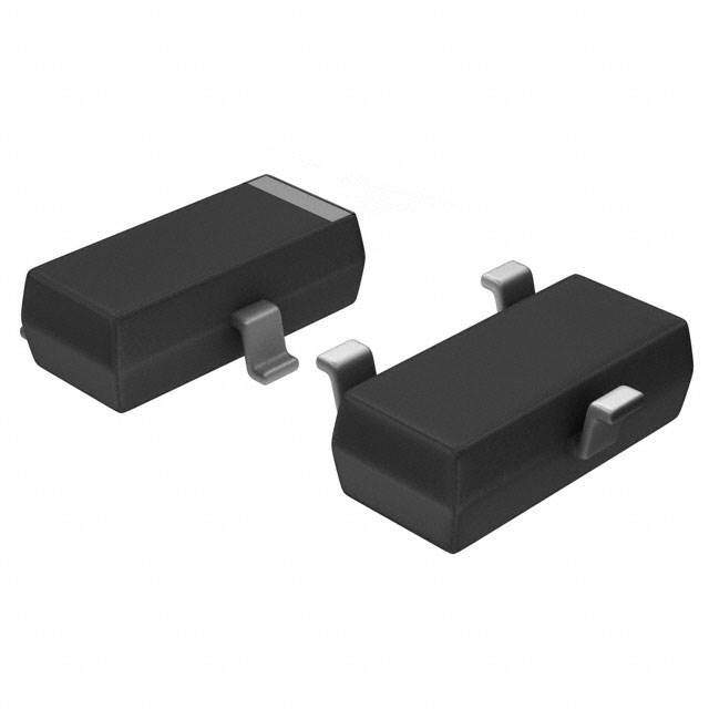
ICGOO电子元器件商城为您提供SDC15.TCT由SEMTECH设计生产,在icgoo商城现货销售,并且可以通过原厂、代理商等渠道进行代购。 SDC15.TCT价格参考¥2.14-¥2.14。SEMTECHSDC15.TCT封装/规格:TVS - 二极管, 21.2V Clamp 10A (8/20µs) Ipp Tvs Diode Surface Mount SOT-23-3。您可以下载SDC15.TCT参考资料、Datasheet数据手册功能说明书,资料中有SDC15.TCT 详细功能的应用电路图电压和使用方法及教程。
Semtech Corporation的SDC15.TCT是一款瞬态电压抑制(TVS)二极管,属于TVS二极管类别,主要用于电子设备中的静电放电(ESD)保护。该器件采用紧凑型封装,具备低电容特性,适用于高速数据接口的信号完整性保护。

SDC15.TCT典型应用场景包括:便携式消费类电子产品如智能手机、平板电脑和可穿戴设备,用于保护USB接口(如USB 2.0、USB Type-C)、HDMI端口、音频插孔等高速信号线路免受ESD冲击;也可应用于笔记本电脑、数码相机和其他带有敏感数据接口的设备中。其快速响应时间和高可靠性使其符合IEC 61000-4-2国际ESD标准(通常支持±15kV空气放电和接触放电),能有效吸收瞬态过电压,防止下游集成电路损坏。

此外,SDC15.TCT因其小型化设计,适合空间受限的高密度PCB布局,广泛用于需要高性能电磁兼容(EMC)防护的终端产品中。总体而言,该TVS二极管适用于对ESD防护要求严苛、信号速率较高且注重可靠性的消费电子与通信设备领域。
| 参数 | 数值 |
| 产品目录 | |
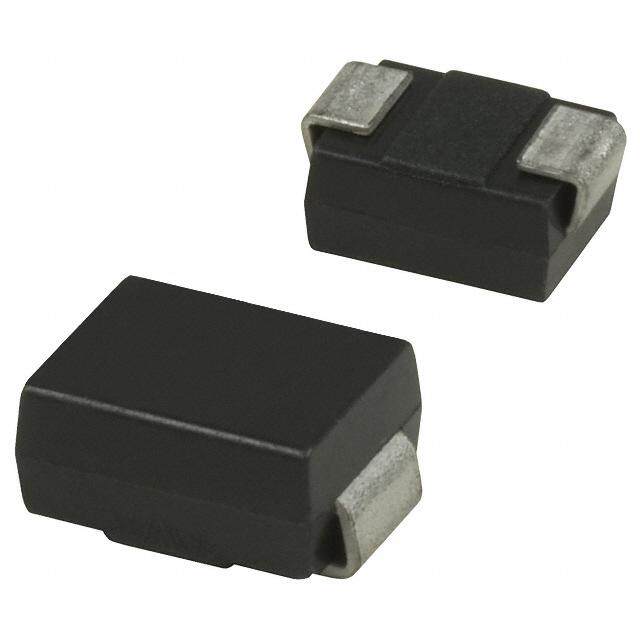
| 描述 | TVS DIODE 12.8VWM 21.2VC SOT23 |
| 产品分类 | |
| 品牌 | Semtech |
| 数据手册 | |
| 产品图片 |
|
| 产品型号 | SDC15.TCT |
| rohs | 无铅 / 符合限制有害物质指令(RoHS)规范要求 |
| 产品系列 | - |
| 不同频率时的电容 | 120pF @ 1MHz |
| 产品目录页面 | |
| 供应商器件封装 | SOT-23-3 |
| 其它名称 | SDC15DKR |
| 功率-峰值脉冲 | 300W |
| 包装 | Digi-Reel® |
| 单向通道 | 2 |
| 双向通道 | - |
| 安装类型 | 表面贴装 |
| 封装/外壳 | TO-236-3,SC-59,SOT-23-3 |
| 工作温度 | -55°C ~ 125°C (TJ) |
| 应用 | 通用 |
| 标准包装 | 1 |
| 电压-击穿(最小值) | 14.3V |
| 电压-反向关态(典型值) | 12.8V (最小值) |
| 电压-箝位(最大值)@Ipp | 21.2V |
| 电流-峰值脉冲(10/1000µs) | 10A (8/20µs) |
| 电源线路保护 | 无 |
| 类型 | 齐纳 |


- 商务部:美国ITC正式对集成电路等产品启动337调查
- 曝三星4nm工艺存在良率问题 高通将骁龙8 Gen1或转产台积电
- 太阳诱电将投资9.5亿元在常州建新厂生产MLCC 预计2023年完工
- 英特尔发布欧洲新工厂建设计划 深化IDM 2.0 战略
- 台积电先进制程称霸业界 有大客户加持明年业绩稳了
- 达到5530亿美元!SIA预计今年全球半导体销售额将创下新高
- 英特尔拟将自动驾驶子公司Mobileye上市 估值或超500亿美元
- 三星加码芯片和SET,合并消费电子和移动部门,撤换高东真等 CEO
- 三星电子宣布重大人事变动 还合并消费电子和移动部门
- 海关总署:前11个月进口集成电路产品价值2.52万亿元 增长14.8%


PDF Datasheet 数据手册内容提取
SDC15 TVS Diode Array for ESD Protection of 12V Data and Power Lines PPRROOTTEECCTTIIOONN PPRROODDUUCCTTSS Description Features The SDC15 transient voltage suppressor (TVS) is (cid:139) 300 watts peak pulse power (t = 8/20µs) p designed to protect components which are connected (cid:139) 40 watts peak pulse power (t = 10/1000µs) to data and transmission lines from voltage surges p (cid:139) Transient protection for data and power lines to caused by electrostatic discharge (((((EEEEESSSSSDDDDD))))), electrical fast IEC 61000-4-2 (ESD) ±15kV (air), ±8kV (contact) transients (((((EEEEEFFFFFTTTTT))))) , and llllliiiiiggggghhhhhtttttnnnnniiiiinnnnnggggg. IEC 61000-4-4 (EFT) 40A (5/50ns) TVS diodes are characterized by their high surge IEC 61000-4-5 (Lightning) 12A (1.2/50µs) capability, low operating and clamping voltages, and (cid:139) Protects one bidirectional line fast response time. This makes them ideal for use as (cid:139) Low clamping voltage board level protection of sensitive semiconductor (cid:139) Low leakage current components. The dual-junction common-cathode (cid:139) High surge capability design allows the user to protect one data or power (cid:139) Solid-state silicon avalanche technology line operating at ±12 volts. The low profile SOT23 package allows flexibility in the design of “crowded” Mechanical Characteristics circuit boards. (cid:139) JEDEC SOT23 package The SDC15 TVS will meet the surge requirements of (cid:139) Molding compound flammability rating: UL 94V-0 IEC 61000-4-2 (Formerly IEC 801-2), Level 4, “Human (cid:139) Marking : DC15 Body Model” for air and contact discharge. (cid:139) Packaging : Tape and Reel per EIA 481 Applications (cid:139) RS-232 Data Lines (cid:139) Portable Electronics (cid:139) Industrial Controls (cid:139) Set-Top Box (cid:139) Servers, Notebook, and Desktop PC (cid:139) 12V DC Supply Protection Circuit Diagram Schematic & PIN Configuration SOT23 (Top View) Revision 12/15/04 1 www.semtech.com
SDC15 PPRROOTTEECCTTIIOONN PPRROODDUUCCTTSS Absolute Maximum Rating Rating Symbol Value Units PeakPulsePower (tp = 8/20µs) P 300 Watts pk PeakPulseCurrent (tp = 8/20µs) I 10 A PP Non-RepetitivePeakForward Current(tp=100µs) I 4 A FSMAX Thermal Resistance,Junction toAmbient θ 556 °C/W JA Lead Soldering Temperature T 260 (10 sec.) °C L Operating Temperature T -55 to+125 °C J StorageTemperature T -55 to+150 °C STG Electrical Characteristics SDC15 Parameter Symbol Conditions Minimum Typical Maximum Units ReverseStand-Off Voltage V 12.8 V RWM ReverseBreakdown Voltage V I= 1mA, 14.3 16.4 V BR t Between Pin 1 and 2 (each direction) ReverseLeakageCurrent I V = 12.8V, T=25°C 100 nA R RWM Between Pin 1 and 2 (each direction) Forward Voltage V I= 100mA, 1.3 V F F Pin 1 to3 and Pin 2 to3 TemperatureCoefficientof VBR αVBR 12 mV/°C Clamping Voltage V I = 1.9A, 21.2 V C PP tp = 10/10000µs Between Pin 1 and 2 (each direction) Junction Capacitance C V = 0V, f = 1MHz 120 pF j R Pin 1 to2 2004 Semtech Corp. 2 www.semtech.com
SDC15 PROTECTION PRODUCTS Typical Characteristics Non-Repetitive Peak Pulse Power vs. Pulse Time Power Derating Curve 10 110 100 W) 90 P (kpk 1 or IPP 80 er - wer 70 w o 60 Po d P 50 k Pulse 0.1 % of Rate 3400 a e 20 P 10 0 0.01 0 25 50 75 100 125 150 0.1 1 10 100 1000 Ambient Temperature - TA (oC) Pulse Duration - t (µs) p Pulse Waveform Clamping Voltage vs. Peak Pulse Current 110 25 Waveform 100 Parameters: 90 tr = 8µs td = 20µs V) 80 (C Percent of IPP 45670000 e-t td = IPP/2 mping Voltage - V 1250 30 a Waveform Cl Parameters: 20 tr = 8µs 10 td = 20µs 10 0 0 5 10 15 20 25 30 1 2 3 4 5 6 7 8 9 10 11 12 Time (µs) Peak Pulse Current - IPP (A) Forward Voltage vs. Forward Current 3 2.5 V) V (F 2 e - g a olt 1.5 V d orwar 1 Waveform F Parameters: 0.5 tr = 8µs td = 20µs 0 0 1 2 3 4 5 6 7 8 9 10 11 12 Forward Current - I (A) F 2004 Semtech Corp. 3 www.semtech.com
SDC15 PPRROOTTEECCTTIIOONN PPRROODDUUCCTTSS Applications Information Device Connection for Protection of One Data Line Device Schematic and Pin Configuration The SDC15 is designed to protect one data or I/O line operating at ±12 volts. Connection options are as follows: (cid:122) Common mode protection: Pin 1 is connected to the data line and pin 2 is connected to ground. For best results, this pin should be connected directly to a ground plane on the board. The path length should be kept as short as possible to minimize parasitic inductance. Pin 3 is not connected. (cid:122) Differential protection: Pin 1 is connected to one line and pin 2 is connected to the second line. Pin 3 is not connected. Circuit Board Layout Recommendations for Suppres- RS-232 Transceiver Protection Example sion of ESD. Good circuit board layout is critical for the suppression of fast rise-time transients such as ESD. The following guidelines are recommended: (cid:122) Place the SDC15 near the input terminals or connectors to restrict transient coupling. (cid:122) Minimize the path length between the SDC15 and the protected line. (cid:122) Minimize all conductive loops including power and ground loops. (cid:122) The ESD transient return path to ground should be kept as short as possible. (cid:122) Never run critical signals near board edges. (cid:122) Use ground planes whenever possible. Matte Tin Lead Finish Matte tin has become the industry standard lead-free replacement for SnPb lead finishes. A matte tin finish is composed of 100% tin solder with large grains. Since the solder volume on the leads is small com- pared to the solder paste volume that is placed on the land pattern of the PCB, the reflow profile will be determined by the requirements of the solder paste. Therefore, these devices are compatible with both lead-free and SnPb assembly techniques. In addition, unlike other lead-free compositions, matte tin does not have any added alloys that can cause degradation of the solder joint. 2004 Semtech Corp. 4 www.semtech.com
SDC15 PROTECTION PRODUCTS Outline Drawing - SOT23 D A DIMENSIONS INCHES MILLIMETERS e1 DIM MIN NOMMAX MINNOMMAX 3 H AA1 ..000305 -- ..000444 00..0819 -- 01..1102 B A2 .035 .037 .040 0.88 0.95 1.02 b .012 - .020 0.30 - 0.51 GAUGE 0 c c .003 - .007 0.08 - 0.18 SEATING PLANE D .110 .114 .120 2.80 2.90 3.04 E PLANE E .082 .093 .104 2.10 2.37 2.64 E1 0.25 E1 .047 .051 .055 1.20 1.30 1.40 C e .075 1.90 BSC L e1 .037 0.95 BSC L1 L .015 .020 .024 0.40 0.50 0.60 DETAIL A L1 .022 (0.55) N 3 3 1 2 0 0° - 8° 0° - 8° aaa .004 0.10 bxN bbb .008 0.20 e bbb C A B A A2 3X aaa C SEE DETAIL A SIDE VIEW SEATING PLANE A1 C NOTES: 1. CONTROLLING DIMENSIONS ARE IN MILLIMETERS (ANGLES IN DEGREES). 2. DATUMS - A - AND - B - TO BE DETERMINED AT DATUM PLANE -H- 3. DIMENSIONS "E1" AND "D" DO NOT INCLUDE MOLD FLASH, PROTRUSIONS OR GATE BURRS. Land Pattern - SOT23 X Y DIMENSIONS DIM INCHES MILLIMETERS C (.087) (2.20) Z G C E .037 0.95 E1 .075 1.90 G .031 0.80 X .039 1.00 Y .055 1.40 Z .141 3.60 Y E E1 NOTES: 1. THIS LAND PATTERN IS FOR REFERENCE PURPOSES ONLY CONSULT YOUR MANUFACTURING GROUP TO ENSURE YOUR COMPANY'S MANUFACTURING GUIDELINES ARE MET. Note 1 : Grid placement cou2.rtyRaEFrEdR EisN C8E xIP C8- SeMl-e78m2Ae.nts (4mm x 4mm) in accordance with the international grid detailed in IEC Publication 97. 2004 Semtech Corp. 5 www.semtech.com
SDC15 PPRROOTTEECCTTIIOONN PPRROODDUUCCTTSS Ordering Information Lead Qtyper Part Number ReelSize Finish Reel SDC15.TC SnPb 3,000 7Inch SDC15.TCT Pb Free 3,000 7Inch Contact Information Semtech Corporation Protection Products Division 200 Flynn Road, Camarillo, CA 93012 Phone: (805)498-2111 FAX (805)498-3804 2004 Semtech Corp. 6 www.semtech.com