 Datasheet下载
- 型号: SP3012-06UTG
- 制造商: Littelfuse
- 库位|库存: xxxx|xxxx
- 要求:
| 数量阶梯 | 香港交货 | 国内含税 |
| +xxxx | $xxxx | ¥xxxx |
查看当月历史价格
查看今年历史价格
SP3012-06UTG产品简介:
ICGOO电子元器件商城为您提供SP3012-06UTG由Littelfuse设计生产,在icgoo商城现货销售,并且可以通过原厂、代理商等渠道进行代购。 SP3012-06UTG价格参考。LittelfuseSP3012-06UTG封装/规格:TVS - 二极管, 。您可以下载SP3012-06UTG参考资料、Datasheet数据手册功能说明书,资料中有SP3012-06UTG 详细功能的应用电路图电压和使用方法及教程。
Littelfuse Inc.生产的SP3012-06UTG是一种TVS(瞬态电压抑制)二极管,广泛应用于各种电子设备中以提供静电放电(ESD)、雷击和其他瞬态过电压保护。以下是该型号的具体应用场景:

1. 通信设备:在路由器、交换机、调制解调器等网络设备中,SP3012-06UTG用于保护数据线和信号线免受瞬态电压的损害。它能够快速响应并钳位过电压,确保通信接口的安全性和稳定性。

2. 消费电子产品:如智能手机、平板电脑、笔记本电脑等便携式设备中,此TVS二极管可以保护USB端口、HDMI接口及其他外部连接点,防止因插入或拔出外设时产生的静电或电压波动对内部电路造成破坏。

3. 工业控制系统:在PLC(可编程逻辑控制器)、传感器、执行器等工业自动化组件里,它可以有效抵御恶劣环境下可能出现的电气干扰,保障系统运行的可靠性和安全性。

4. 汽车电子:现代汽车中的娱乐系统、导航系统、车身控制模块等都需要强大的抗干扰能力。SP3012-06UTG可用于保护CAN总线、LIN总线等车载网络以及电源输入端,避免因外界因素导致的故障。

5. 医疗设备:对于心电图机、超声波仪器等精密医疗设备而言,稳定的电源供应至关重要。该TVS二极管能为这些设备的关键部位提供有效的过压保护,确保其正常工作,同时保护患者安全。

总之,SP3012-06UTG凭借其卓越的性能和可靠性,在众多领域发挥着重要作用,成为众多设计工程师首选的防护元件之一。
| 参数 | 数值 |
| 产品目录 | |
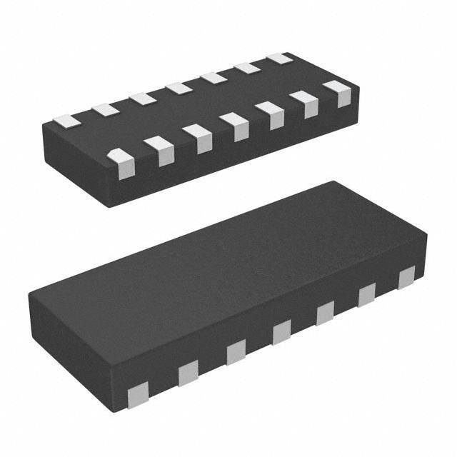
| 描述 | TVS DIODE 5VWM 7VC 14UDFNTVS二极管阵列 6 Ch 12KV 0.5pF |
| 产品分类 | |
| 品牌 | Littelfuse |
| 产品手册 | |
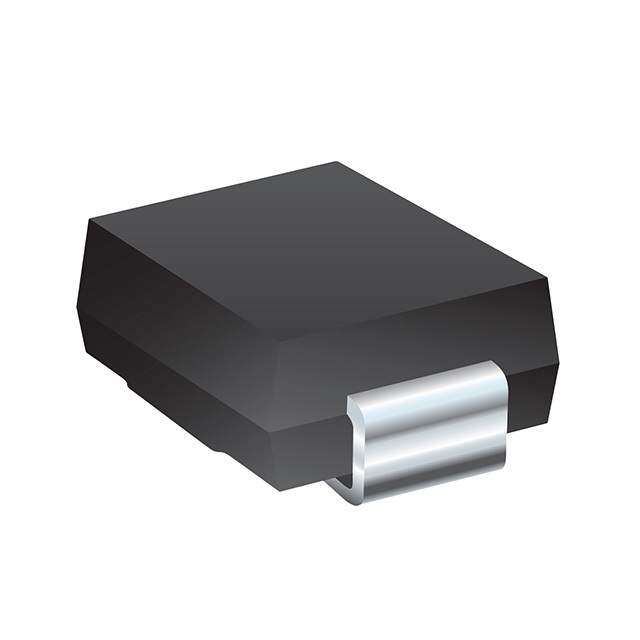
| 产品图片 |
|
| rohs | 符合RoHS无铅 / 符合限制有害物质指令(RoHS)规范要求 |
| 产品系列 | 二极管与整流器,TVS二极管,TVS二极管阵列,Littelfuse SP3012-06UTGSP3012, SPA® |
| 数据手册 | |
| 产品型号 | SP3012-06UTG |
| 不同频率时的电容 | 0.5pF @ 1MHz |
| 产品培训模块 | http://www.digikey.cn/PTM/IndividualPTM.page?site=cn&lang=zhs&ptm=25590 |
| 产品种类 | TVS二极管阵列 |
| 供应商器件封装 | 14-UDFN(3.5x1.35) |
| 其它名称 | F5914TR |
| 功率-峰值脉冲 | - |
| 包装 | 带卷 (TR) |
| 单向通道 | - |
| 双向通道 | 6 |
| 商标 | Littelfuse |
| 商标名 | SPA |
| 安装类型 | 表面贴装 |
| 封装 | Reel |
| 封装/外壳 | 14-UFDFN |
| 封装/箱体 | uDFN |
| 尺寸 | 1.35 mm W x 3.5 mm L x 0.5 mm H |
| 峰值浪涌电流 | 4 A |
| 工作温度 | -40°C ~ 125°C |
| 工作电压 | 6 V |
| 工厂包装数量 | 3000 |
| 应用 | 通用 |
| 最大工作温度 | + 125 C |
| 最小工作温度 | - 55 C |
| 标准包装 | 3,000 |
| 电压-击穿(最小值) | - |
| 电压-反向关态(典型值) | 5V(最小值) |
| 电压-箝位(最大值)@Ipp | 7V (标准) |
| 电容 | 0.5 pF |
| 电流-峰值脉冲(10/1000µs) | 2A (8/20µs) |
| 电源线路保护 | 是 |
| 端接类型 | SMD/SMT |
| 类型 | 转向装置(轨至轨) |
| 系列 | SP3012 |
| 通道 | 6 Channels |
| 钳位电压 | 7 V |


- 商务部:美国ITC正式对集成电路等产品启动337调查
- 曝三星4nm工艺存在良率问题 高通将骁龙8 Gen1或转产台积电
- 太阳诱电将投资9.5亿元在常州建新厂生产MLCC 预计2023年完工
- 英特尔发布欧洲新工厂建设计划 深化IDM 2.0 战略
- 台积电先进制程称霸业界 有大客户加持明年业绩稳了
- 达到5530亿美元!SIA预计今年全球半导体销售额将创下新高
- 英特尔拟将自动驾驶子公司Mobileye上市 估值或超500亿美元
- 三星加码芯片和SET,合并消费电子和移动部门,撤换高东真等 CEO
- 三星电子宣布重大人事变动 还合并消费电子和移动部门
- 海关总署:前11个月进口集成电路产品价值2.52万亿元 增长14.8%


PDF Datasheet 数据手册内容提取
TVS Diode Array (SPA ® Diodes) Low Capacitance ESD Protection - SP3012 Series SP3012 Series 0.5pF Diode Array for USB3.0 RoHS Pb GREEN Description The SP3012 Series integrates either 3, 4 or 6 channels of ultra low capacitance rail-to-rail diodes and an additional zener diode to provide protection for electronic equipment that may experience destructive electrostatic discharges (ESD). These robust devices can safely absorb repetitive ESD strikes above the maximum level specified in the IEC 61000-4-2 international standard (±8kV contact discharge) without performance degradation. The extremely low loading capacitance also makes it ideal for protecting high speed signal lines such as USB3.0, HDMI, USB2.0, and eSATA. Features Pinout *Pins 6, 7, 9, 10 are not internally connected • ESD, IEC 61000-4-2, • Small form factor μDFN but should be connected to the trace. 4 5 6 ±12kV contact, ±25kV air (JEDEC MO-229) and 6 7 8 9 10 • EFT, IEC 61000-4-4, 40A SOT23-6 (JEDEC MO- (t =5/50ns) 178AB) packages provide P flow through routing to • Lightning, IEC 61000- simplify PCB layout 3 2 1 5 4 3 2 1 4-5 2nd edition, 4A SP3012-03UTG SP3012-04UTG (AEC-Q101 Qualified) (t =8/20μs) • AEC-Q101 Qaulified P 8 14 6 5 4 • Low capacitance of 0.5pF • RoHS compliant and lead- (TYP) per I/O free • Low leakage current of 1.5μA (MAX) at 5V 7 1 Applications SP3012-06UTG (AEC-Q101 Qualified) 1 2 3 *Pins 1, 2, 3, 4, 5, 6, 7 are not internally connected but should be connected to the opposite pin SP3012-04HTG • LCD/PDP TVs • Set Top Boxes with the PCB trace. • External Storages • Smartphones Functional Block Diagram • DVD/Blu-ray Players • Ultrabooks/Notebooks • Desktops • Digital Cameras SP3012-03UTG SP3012-06UTG • MP3/PMP • Automotive Electronics Application Example for USB3.0 PIN 1 PIN 11 PIN 8 PIN 4 PIN 12 PIN 13 PIN 9 PIN 5 PIN 14 USB Port USB Controller V BUS GND (PIN 2) PIN 10 SP3012-04UTG SP3012-04HTG SSTX+ SSTX - IC PIN 1 PIN 1 SSRX+ PIN 2 PIN 3 PIN 4 PIN 4 SSRX- PIN 5 PIN 6 GND SP3012 -06UTG D+ GND (PIN 3, 8) GND (PIN 2) D- Additional Information Signal GND Life Support Note: Not Intended for Use in Life Support or Life Saving Applications The products shown herein are not designed for use in life sustaining or life saving Datasheet Resources Samples applications unless otherwise expressly indicated. © 2019 Littelfuse, Inc. Specifications are subject to change without notice. Revised: 09/17/19
TVS Diode Array (SPA ® Diodes) Low Capacitance ESD Protection - SP3012 Series Absolute Maximum Ratings Symbol Parameter Value Units I Peak Current (t=8/20μs) 4.0 A PP p T Operating Temperature -40 to 125 °C OP T Storage Temperature -55 to 150 °C STOR 2 CAUTION: Stresses above those listed in “Absolute Maximum Ratings” may cause permanent damage to the device. This is a stress only rating and operation of the device at these or any other 1 conditions above those indicated in the operational sections of this specification is not implied. 0 3 P Electrical Characteristics (T =25ºC) S OP Parameter Symbol Test Conditions Min Typ Max Units Reverse Standoff Voltage V I ≤ 1µA 5.0 V RWM R Reverse Leakage Current I V=5V, Any I/O to GND 1.5 µA LEAK R I =1A, t=8/20µs, Fwd 6.6 7.9 V Clamp Voltage1 V PP p C I =2A, t=8/20µs, Fwd 7.0 8.4 V PP p Dynamic Resistance R (V - V ) / (I - I ) 0.4 Ω DYN C2 C1 PP2 PP1 IEC61000-4-2 (Contact) ±12 kV ESD Withstand Voltage1 V ESD IEC61000-4-2 (Air) ±25 kV Diode Capacitance1 C Reverse Bias=0V, f=1 MHz 0.5 0.65 pF I/O-GND Diode Capacitance1 C Reverse Bias=0V, f=1 MHz 0.3 0.4 pF I/O-/O Note: 1 Parameter is guaranteed by design and/or device characterization. Capacitance vs. Bias Voltage Insertion Loss (S21) I/O to GND 1.0 0 -3 0.8 -6 Capacitance (pF)00..46 Attenuation (dB)---111-9852 -21 0.2 -24 -27 0.0 -30 0.0 1.0 2.0 3.0 4.0 5.0 100 Frequency (MHz) 1000 Bias Voltage (V) Clamping Voltage vs. I Transmission Line Pulsing(TLP) Plot PP 15 14 10.0 13 12 8.0 )A11 ( tn10 e 9 6.0 rruC 8 P 7 L T 6 e (V)4.0 5 g 4 a olt 3 p V2.0 2 m a 1 Cl 0.0 0 1 2 Current (A) 3 4 0 1 2 3 4 5 6 7 8 9 10 11 TLP Voltage (V) © 2019 Littelfuse, Inc. Specifications are subject to change without notice. Revised: 09/17/19
TVS Diode Array (SPA ® Diodes) Low Capacitance ESD Protection - SP3012 Series Pulse Waveform Product Characteristics Pre-Plated Frame (µDFN) Lead Plating 110% Matte Tin (SOT23) 100% Lead Material Copper Alloy 90% Lead Coplanarity 0.0004 inches (0.102mm) 80% Substitute Material Silicon of IPP 6700%% Body Material Molded Epoxy ent 50% Flammability UL 94 V-0 Perc 40% Notes : 30% 1. All dimensions are in millimeters 20% 2. Dimensions include solder plating. 3. Dimensions are exclusive of mold flash & metal burr. 10% 4. Blo is facing up for mold and facing down for trim/form, i.e. reverse trim/form. 0% 5. Package surface matte finish VDI 11-13. 0.0 5.0 10.0 15.0 20.0 25.0 30.0 Time (μs) Soldering Parameters Reflow Condition Pb – Free assembly tP - Temperature Min (Ts(min)) 150°C TP CCrriittiiccaall ZZoonnee Pre Heat - Temperature Max (Ts(max)) 200°C e RRaammpp--uupp TTLL ttoo TTPP ATvera gtoe Tra m- Rp- Ta umimpp er-a u(tmpe iR(nLa ittqoeu midauxs)) ( Ttes)mp (TL) to peak 6330°°CC –// ss1ee8cc0oo nnsdde cmmsaaxx rutarepm TS(mTaxL) tL RRaammpp--ddoown S(max) L e PPrreehheeaatt T Reflow -- TTeemmppeerraattuurree ((TtL)) (Liquidus) 26107 –° C1 50 seconds TS(min) tS L Peak Temperature (T) 260+0/-5 °C P 25 Time within 5°C of actual peak Temperature (tp) 20 – 40 seconds time to peak temperature Time Ramp-down Rate 6°C/second max Time 25°C to peak Temperature (T) 8 minutes Max. P Do not exceed 260°C Ordering Information Part Numbering System SP 3012 –xx x T G Part Number Package Min. Order Qty. TVS Diode Arrays SP3012-03UTG µDFN-6 3000 (SPA® Diodes) G= Green SP3012-04UTG µDFN-10 3000 SP3012-06UTG µDFN-14 3000 T= Tape & Reel SP3012-04HTG SOT23-6 3000 Series Package Number of Channels U= µDFN-6 (1.6x1.6mm) 03 = 3 channel µDFN-10 (2.5x1.0mm) 04 = 4 channel µDFN-14 (3.5x1.35mm) Part Marking System 06 = 6 channel H= SOT23-6 (3.0x1.75mm) V * * Product Series Number of V = SP3012 Channels Assembly Site 3 = 3 channel 4 = 4 channel 6 = 6 channel © 2019 Littelfuse, Inc. Specifications are subject to change without notice. Revised: 09/17/19
TVS Diode Array (SPA ® Diodes) Low Capacitance ESD Protection - SP3012 Series Application Information Signal Integrity of High-Speed Data Interfaces Figure 1: PCB Layout of the SP3012-06UTG for USB 3.0 Adding external ESD protection to a high-speed data port is not trivial for a variety of reasons. J1 1. ESD protection devices will add parasitic capacitance to each data line from line to GND and line to line causing impedance mismatches between the differential pairs. This ultimately affects the signal eye-diagram and whether or not the transceiver can distinguish a “1” from a “0”. U1 2. ESD devices should be placed as close as possible to the port being protected to maximize their effect (i.e. clamping capability) and minimize the effect that PCB trace inductance can have during an ESD transient. Depending on the package size and pinout this could be challenging Figure 2 shows the USB 3.0 eye diagram that resulted and the bigger the package, the larger the land pattern from the PCB layout above with the SP3012-06UTG must be, which adds more parasitic capacitance. soldered on the landing pattern. 3. Stub traces can add another element of discontinuity 500 adversely affecting signal integrity so ESD protection is best employed when it’s “overlaid” on the data lines or when the signals can simply pass underneath the device. Taking all of this into account Littelfuse developed the SP3012 Series which was designed specifically 0 for protection of high-speed data ports such as HDMI 1.3/1.4 and USB 3.0. They present less than 0.5pF from line to GND and only 0.3pF from line to line minimizing impedance mismatch between the differential pairs. Wfrms:500 Furthermore, the SP3012 is rated up to ±12kV (contact -500 Base: 27.0000 ns Scale:33.0 ps/div discharge) which far exceeds the maximum requirement of the IEC 61000-4-2 standard. Figure 2: USB 3.0 Eye Diagram with the SP3012-06UTG There are two options available (4 channel and 6 channel) and both are housed in leadless µDFN packages so the Using a similar layout as above, Figure 3 shows the eye data lines can pass directly underneath the device to diagram that resulted using the SP3012-04UTG to protect reduce discontinuities and maintain signal integrity. the Super-Speed data lines and the SP3003-02UTG to protect the legacy data pair. 500 USB 3.0 Eye Diagram Data Figure 1 shows the layout used for the SP3012-06UTG in a USB 3.0 application. The traces routed toward the top are the two legacy USB 2.0 lines (D+/D-) that run at the slower speed of 480Mbps and therefore are not as critical as the 0 5Gbps Super-Speed traces. Wfrms:850 -500 Base: 27.0000 ns Scale:33.0 ps/div Figure 3: USB 3.0 Eye Diagram with the SP3012-04UTG © 2019 Littelfuse, Inc. Specifications are subject to change without notice. Revised: 09/17/19
TVS Diode Array (SPA ® Diodes) Low Capacitance ESD Protection - SP3012 Series Package Dimensions — μDFN-6 Bottom View Top View Package μDFN-6 (1.6x1.6x0.5mm) D2 JEDEC MO-229 D A 0.05 C Millimeters Inches L Symbol 6 5 4 4 5 6 0.05 C Min Max Min Max A 0.45 0.55 0.018 0.022 E A1 0.00 0.05 0.000 0.002 A3 0.152Ref 0.006 Ref E2 Pin 1 Index Area 1 2 3 3 2 1 Pin 1 chamfer b 0.20 0.30 0.008 0.012 B 0.10 x 45’ D 1.55 1.65 0.061 0.065 ℮ D2 1.05 1.30 0.042 0.052 E 1.50 1.70 0.060 0.067 Side View E2 0.40 0.65 0.016 0.026 0.05 C A1 A3 e 0.50 BSC 0.020BSC A Seating plane L 0.164 0.316 0.006 0.012 C b 0.10 M C AB 0.05 M C Embossed Carrier Tape & Reel Specification — μDFN-6 D Millimetres Inches Symbol P2 t Min Max Min Max E 1.65 1.85 0.06 0.07 F 3.45 3.55 0.14 0.14 E D1 1.00 1.25 0.04 0.05 D 1.50 MIN 0.06 MIN W P0 3.90 4.10 0.15 0.16 10P0 40.0+/- 0.20 1.57+/-0.01 W 7.90 8.30 0.31 0.33 P2 1.95 2.05 0.08 0.08 F A0 1.78 1.88 0.07 0.07 0 D1 B B0 1.78 1.88 0.07 0.07 P0 K0 0.84 0.94 0.03 0.04 t 0.25 TYP 0.01 TYP A0 0 K © 2019 Littelfuse, Inc. Specifications are subject to change without notice. Revised: 09/17/19
TVS Diode Array (SPA ® Diodes) Low Capacitance ESD Protection - SP3012 Series Package Dimensions— µDFN-10 (2.5x1.0x0.5mm) Top View Package µDFN-10 (2.5x1.0x0.5mm) Top View D A JEDEC MO-229 D A Millimeters Inches E Symbol Min Nom Max Min Nom Max A 0.48 0.515 0.55 0.019 0.020 0.021 E B Side View A1 0.00 -- 0.05 0.000 0.022 0.05 C A1 A3 A3 0.125 Ref 0.005 Ref Seating A B b 0.15 0.20 0.25 0.006 0.008 0.012 Plane b1 0.05 C SideC View b b1 0.35 0.40 0.45 0.014 0.016 0.018 0.05 C A10.1A03M C A B D 2.40 2.50 2.60 0.094 0.098 0.102 A 0.05 M C E 0.90 1.00 1.10 0.035 0.039 0.043 Seating e 0.50 BSC 0.020 BSC Plane b1 Bottom Vie0.w05 C L 0.30 0.365 0.43 0.012 0.014 0.016 C b R0.125 0.10 MLC A B Soldering Pad Layout Dimensions 0.05 M C 2xR0.075mm (7x) Symbol Inch Millimeter e C (0.034) (0.875) Recomended G 0.008 0.20 Bottom VieSwoldering Pad Layout R0.125 P P1 P 0.020 0.50 P1 0.039 1.00 Y X 0.008 0.20 Z (C) G (Y1) X1 0.016 0.40 L Y 0.027 0.675 X 2xR0.075mm (7x) X1 Y1 (0.061) (1.55) e Z 0.061 1.55 Recomended Alternative Soldering Pad Layout Soldering Pad Layout P1 P1 P P Y Y Z (C) G (Y1) Z (C) G (Y1) X X X1 X1 Embossed Carrier Tape & Reel Specification— µDFN-10 P0 Package µDFN-10 (2.5x1.0x0.5mm) P1 D0 T User Feeding Direction Symbol Millimeters P2 A0 1.30 +/- 0.10 E B0 2.83 +/- 0.10 W D0 Ø 1.50 + 0.10 D1 Ø 1.00 + 0.25 F E 1.75 +/- 0.10 D1 B0 5º Max Pin 1 Location F 3.50 +/- 0.05 K0 0.65 +/- 0.10 A0 P0 4.00 +/- 0.10 P1 4.00 +/- 0.10 5º Max P2 2.00 +/- 0.05 K0 T 0.254 +/- 0.02 W 8.00 + 0.30 /- 0.10 © 2019 Littelfuse, Inc. Specifications are subject to change without notice. Revised: 09/17/19
TVS Diode Array (SPA ® Diodes) Low Capacitance ESD Protection - SP3012 Series Package Dimensions — µDFN-14 (3.5x1.35x0.5mm) Top View µDFN-14 (3.5x1.35x0.5mm) D A JEDEC MO-229 Millimeters Inches Symbol E Min Nom Max Min Nom Max A 0.45 0.50 0.55 0.018 0.020 0.022 PIN 1 Index Area 1 2 3 4 B A1 0.00 0.02 0.05 0.000 0.001 0.002 A2 0.203 Ref 0.008 Ref Side View b 0.15 0.20 0.25 0.006 0.008 0.012 A1 A2 D 3.40 3.50 3.60 0.134 0.138 0.142 Seating A D2 - - - - - - Plane E 1.25 1.35 1.45 0.050 0.054 0.058 b C E1 - - - - - - e 0.500 BSC 0.020 BSC L 0.25 0.30 0.35 0.010 0.012 0.014 Notes: Bottom View 1. Dimension and tolerancing comform to ASME Y14.5M-1994. 2. Controlling dimensions: Millimeter. Converted Inch dimensions are not necessarily exact. Soldering Pad Layout Dimensions Millimeters Inches Pin 1 Identification Symbol Nom Nom Chamfer 0.10X45º D 3.30 0.1299 E 1.65 0.0571 b 0.30 0.0118 L 0.50 0.0197 e 0.50 typ 0.020 typ Recomended s 0.20 0.0078 Soldering Pad Layout s1 0.65 0.0256 Symbol Millimeter Inches Embossed Carrier Tape & Reel Specification — µDFN-14 Symbol Millimeters PP21 P0 D0 E User Feeding Direction A0 1.58 +/- 0.10 B0 3.73 +/- 0.10 D0 Ø 1.50 + 0.10 D1 Ø 0.60 +/- 0.05 F E 1.75 +/- 0.10 W Pin 1 Location F 5.50 +/- 0.05 K0 0.68 + 0.12/ -0.10 D1 A0 P0 2.00 +/- 0.05 T P1 4.00 +/- 0.10 P2 4.00 +/- 0.10 K0 B0 T 0.28 +0.02/ -0.05 W 12.00 + 0.30 /- 0.10 © 2019 Littelfuse, Inc. Specifications are subject to change without notice. Revised: 09/17/19
TVS Diode Array (SPA ® Diodes) Low Capacitance ESD Protection - SP3012 Series Package Dimensions — SOT23-6 Package SOT23 Pins 6 JEDEC MO-178AB Millimeters Inches Symbol Notes Min Max Min Max A 0.900 1.450 0.035 0.057 - A1 0.000 0.150 0.000 0.006 - A2 0.900 1.300 0.035 0.051 - b 0.350 0.500 0.0138 0.0196 - C 0.080 0.220 0.0031 0.009 - D 2.800 3.000 0.11 0.118 3 E 2.600 3.000 0.102 0.118 - E1 1.500 1.750 0.06 0.069 3 e 0.95 Ref 0.0374 ref - e1 1.9 Ref 0.0748 Ref - L 0.30 0.600 0.012 0.023 4,5 N 6 6 6 a 0º 8º 0º 8º - Recommended Solder Pad Layout M 2.590 0.102 - O 0.690 .027 TYP - P 0.990 .039 TYP - R 0.950 0.038 - Notes: M 1. Dimensioning and tolerancing Per ASME Y14.5M-1994. 2. Package conforms to EIAJ SC-74 (1992). 3. Dimensions D and E1 are exclusive of mold flash, protrusions, or gate burrs. 4. Foot length L measured at reference to seating plane. P 5. “L” is the length of flat foot surface for soldering to substrate. 6. “N” is the number of terminal positions. 7. Controlling dimension: MILLIMETER. Converted inch dimensions are not necessarily exact. R O Embossed Carrier Tape & Reel Specification — SOT23-6 8mm TAPE AND REEL 14.4mm 4.0mm ACCESS HOLE 1.5mm 2.0mm 1.75mm DIA. HOLE 13mm 8mm CL 4.0mm 180mm 60mm GENERAL INFORMA TION SOT-23 (8mm POCKET PITCH) 1. 3000 PIECES PER REEL. 2. ORDER IN MUL TIPLES OF FULL REELS ONLY. 3. MEETS EIA-481 REVISION "A" SPECIFICATIONS. 8.4mm USER DIRECTION OF FEED PIN 1 Disclaimer Notice - Information furnished is believed to be accurate and reliable. However, users should independently evaluate the suitability of and test each product selected for their own applications. Littelfuse products are not designed for, and may not be used in, all applications. Read complete Disclaimer Notice at http://www.littelfuse.com/disclaimer-electronics. © 2019 Littelfuse, Inc. Specifications are subject to change without notice. Revised: 09/17/19 COVER TAPE