 Datasheet下载
- 型号: RCLAMP3304P.TCT
- 制造商: SEMTECH
- 库位|库存: xxxx|xxxx
- 要求:
| 数量阶梯 | 香港交货 | 国内含税 |
| +xxxx | $xxxx | ¥xxxx |
查看当月历史价格
查看今年历史价格
RCLAMP3304P.TCT产品简介:
ICGOO电子元器件商城为您提供RCLAMP3304P.TCT由SEMTECH设计生产,在icgoo商城现货销售,并且可以通过原厂、代理商等渠道进行代购。 RCLAMP3304P.TCT价格参考。SEMTECHRCLAMP3304P.TCT封装/规格:TVS - 二极管, 16V Clamp 5A (8/20µs) Ipp Tvs Diode Surface Mount SLP1616P6 (1.6x1.6)。您可以下载RCLAMP3304P.TCT参考资料、Datasheet数据手册功能说明书,资料中有RCLAMP3304P.TCT 详细功能的应用电路图电压和使用方法及教程。
RCLAMP3304P.TCT是Semtech Corporation推出的一款瞬态电压抑制(TVS)二极管,属于低电容、高可靠性保护器件,广泛应用于各类电子设备的静电放电(ESD)和浪涌保护。该器件具有快速响应、低钳位电压和高脉冲吸收能力的特点,适用于对信号完整性要求较高的场景。

典型应用场景包括:便携式消费类电子产品(如智能手机、平板电脑、笔记本电脑)中的高速数据接口保护,例如USB 2.0/3.0、HDMI、DisplayPort等;通信设备中的以太网端口、RS-232/RS-485接口;工业控制系统的信号线与电源线防护;以及智能家居、可穿戴设备中的敏感电路防静电设计。其低电容特性(通常小于1pF)确保了对高速信号传输的干扰最小,保障信号质量。

此外,RCLAMP3304P.TCT采用小型化封装(如DFN),节省PCB空间,适合高密度布局的现代电子产品。工作温度范围宽(-40°C至+125°C),可在严苛环境下稳定运行,增强了系统可靠性。整体而言,该TVS二极管是高速、高灵敏度电子接口抵御瞬态过压的理想选择。
| 参数 | 数值 |
| 产品目录 | |
| 描述 | TVS DIODE 3.3VWM 16VC SLP1616P6 |
| 产品分类 | |
| 品牌 | Semtech |
| 数据手册 | |
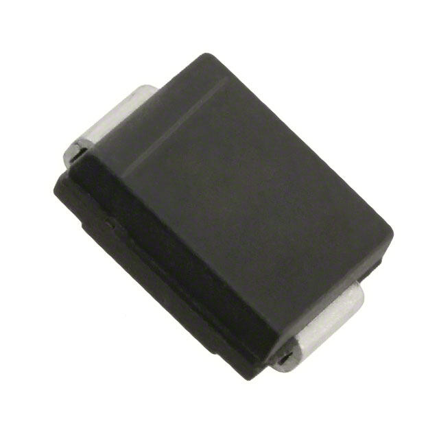
| 产品图片 |
|
| 产品型号 | RCLAMP3304P.TCT |
| rohs | 无铅 / 符合限制有害物质指令(RoHS)规范要求 |
| 产品系列 | RailClamp® |
| 不同频率时的电容 | 0.8pF @ 1MHz |
| 产品目录页面 | |
| 供应商器件封装 | SLP1616P6(1.6x1.6) |
| 其它名称 | RCLAMP3304PTCT |
| 功率-峰值脉冲 | 80W |
| 包装 | 带卷 (TR) |
| 单向通道 | - |
| 双向通道 | 4 |
| 安装类型 | 表面贴装 |
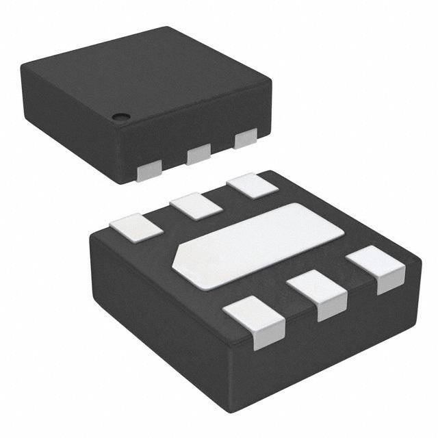
| 封装/外壳 | 6-UFDFN 裸露焊盘 |
| 工作温度 | -40°C ~ 85°C (TJ) |
| 应用 | 医疗卡接口 |
| 标准包装 | 3,000 |
| 电压-击穿(最小值) | 3.5V |
| 电压-反向关态(典型值) | 3.3V (最小值) |
| 电压-箝位(最大值)@Ipp | 16V |
| 电流-峰值脉冲(10/1000µs) | 5A (8/20µs) |
| 电源线路保护 | 是 |
| 类型 | 转向装置(轨至轨) |


- 商务部:美国ITC正式对集成电路等产品启动337调查
- 曝三星4nm工艺存在良率问题 高通将骁龙8 Gen1或转产台积电
- 太阳诱电将投资9.5亿元在常州建新厂生产MLCC 预计2023年完工
- 英特尔发布欧洲新工厂建设计划 深化IDM 2.0 战略
- 台积电先进制程称霸业界 有大客户加持明年业绩稳了
- 达到5530亿美元!SIA预计今年全球半导体销售额将创下新高
- 英特尔拟将自动驾驶子公司Mobileye上市 估值或超500亿美元
- 三星加码芯片和SET,合并消费电子和移动部门,撤换高东真等 CEO
- 三星电子宣布重大人事变动 还合并消费电子和移动部门
- 海关总署:前11个月进口集成电路产品价值2.52万亿元 增长14.8%


PDF Datasheet 数据手册内容提取
RClamp2504P & RClamp3304P RailClamp®®®®® 2.5V & 3.3V TVS Arrays ®®®®® PROTECTION PRODUCTS - RailClamp Description Features RailClamp® is a low capacitance TVS array designed to (cid:139) Transient protection for high-speed data lines to protect high speed data interfaces. This series has been IEC 61000-4-2 (ESD) ±15kV (air), ±8kV (contact) specifically designed to protect sensitive components IEC 61000-4-4 (EFT) 40A (5/50ns) which are connected to data and transmission lines from (cid:139) Array of surge rated diodes with internal TVS Diode overvoltage caused by ESD (electrostatic discharge), CDE (cid:139) Small package saves board space (Cable Discharge Events), and EFT (electrical fast tran- (cid:139) Protects up to four I/O lines sients). (cid:139) Low capacitance (<0.8pF) for high-speed interfaces The monolithic design incorporates surge rated, low (cid:139) Minimal insertion loss to 33333.....00000GGGGGHHHHHzzzzz capacitance steering diodes and a TVS diode in a single (cid:139) Low operating voltage: 2.5V and 3.3V package. Each line has a maximum capacitance of (cid:139) Low leakage current and clamping voltage < 0.8pF to ground. The capacitance of each line is well (cid:139) Solid-state silicon-avalanche technology matched for consistant signal balance. This device is Mechanical Characteristics optimized for ESD protection of portable electronics. It may be used to meet the ESD immunity requirements (cid:139) SLP1616P6 package of IEC 61000-4-2, Level 4 (±15kV air, ±8kV contact (cid:139) RoHS/WEEE Compliant discharge). (cid:139) Nominal Dimensions: 1.6 x 1.6 x 0.58 mm The RClampTM2504P and RClampTM3304P are con- (cid:139) Lead Finish: NiPdAu structed using Semtech’s proprietary EPD process (cid:139) Molding compound flammability rating: UL 94V-0 technology. The EPD process provides low standoff (cid:139) Marking: Marking Code + Date Code voltages with significant reductions in leakage current (cid:139) Packaging: Tape and Reel and capacitance over silicon-avalanche diode pro- cesses. They feature a true operating voltage of 2.5 Applications volts and 3.3 volts for superior protection. (cid:139) Multi Media Card (MMC) Interfaces These devices are in a 6-pin, RoHS/WEEE compliant, (cid:139) SATA Interfaces SLP1616P6 package measuring 1.6 x 1.6 x 0.58mm. (cid:139) SD Card Interfaces The leads are spaced at a pitch of 0.5mm and are (cid:139) SIM Ports finished with lead-free NiPdAu. (cid:139) MDDI Ports (cid:139) MPPI Ports Circuit Diagram Pin Configuration 1.6 1 3 1.6 6 1 2 5 6 0.5 0.58 GND SLP1616P6 (Bottom View) Nominal Dimensions in mm Revision 01/15/2008 1 www.semtech.com
RClamp2504P & RClamp3304P PROTECTION PRODUCTS Absolute Maximum Rating Rating Symbol Value Units PeakPulsePower(tp =8/20μs) P 80 Watts pk PeakPulseCurrent (tp =8/20μs) I 5 A PP ESDperIEC61000-4-2(Air) V 20 kV ESD ESDperIEC61000-4-2(Contact) 12 Operating Temperature T -40to+85 °C J StorageTemperature T -55to+150 °C STG Electrical Characteristics (T=25oC) RClamp2504P Parameter Symbol Conditions Minimum Typical Maximum Units ReverseStand-Off Voltage V Pin 3toGND 2.5 V RWM Punch-Through Voltage V I =2μA 2.7 V PT PT Snap-BackVoltage V I =50mA 2.0 V SB SB ReverseLeakageCurrent I V =2.5V,T=25°C 0.5 μA R RWM Clamping Voltage V I =1A,t =8/20μs 6.5 V C PP p Clamping Voltage V I =5A,t =8/20μs 13 V C PP p Junction Capacitance C VR =0V,f =1MHz 0.8 pF j Any I/Opin toGND VR =0V,f =1MHz 0.4 pF Between I/Opins © 2008 Semtech Corp. 2 www.semtech.com
RClamp2504P & RClamp3304P PROTECTION PRODUCTS RClamp3304P Parameter Symbol Conditions Minimum Typical Maximum Units ReverseStand-Off Voltage V Pin 3toGND 3.3 V RWM Punch-Through Voltage V I =2μA 3.5 V PT PT Snap-Back Voltage V I =50mA 2.8 V SB SB ReverseLeakageCurrent I V =3.3V, T=25°C 0.5 μA R RWM Clamping Voltage V I =1A, t =8/20μs 7.5 V C PP p Any I/OGND Clamping Voltage V I =5A, t =8/20μs 16 V C PP p Any I/OtoGND Junction Capacitance C VR =0V, f =1MHz 0.8 pF j Any I/Opin toGND VR =0V, f =1MHz 0.4 pF Between I/Opins © 2008 Semtech Corp. 3 www.semtech.com
RClamp2504P & RClamp3304P PROTECTION PRODUCTS Typical Characteristics Non-Repetitive Peak Pulse Power vs. Pulse Time Power Derating Curve 10 110 100 W) 90 wer - P (kPP 1 Power or IPP 678000 k Pulse Po 0.1 % of Rated 345000 a e 20 P 10 0 0.01 0 25 50 75 100 125 150 0.1 1 10 100 1000 Pulse Duration - tp (us) Ambient Temperature - TA (oC) Pulse Waveform Normalized Capacitance vs. Reverse Voltage 110 1.2 Waveform 100 Parameters: 90 tr = 8µs 1 80 td = 20µs of IPP 6700 e-t V=0)R0.8 Percent 4500 td = I /2 V) / C(RJ0.6 30 PP C(J0.4 20 10 0.2 0 f = 1 MHz 0 5 10 15 20 25 30 0 0 0.5 1 1.5 2 2.5 3 3.5 Time (µs) Reverse Voltage - VR (V) Clamping Voltage vs. Peak Pulse Current Clamping Voltage vs. Peak Pulse Current I/O to GND I/O to I/O 15 20 RClamp3304P (V)C (V)C15 RClamp3304P e - V 10 e - V g g a a olt olt 10 V RClamp2504P V RClamp2504P g g n n pi 5 pi m Waveform m Waveform Cla Parameters: Cla 5 Parameters: tr = 8μs tr = 8μs td = 20μs td = 20μs 0 0 0 1 2 3 4 5 6 0 1 2 3 4 5 6 Peak Pulse Current - IPP (A) Peak Pulse Current - IPP (A) © 2008 Semtech Corp. 4 www.semtech.com
RClamp2504P & RClamp3304P PROTECTION PRODUCTS Typical Characteristics Insertion Loss S21 (I/O to Gnd) Analog Crosstalk CH1 S21 LOG 20 dB /R EF 0 dB CH1 S21 LOG 6 dB / REF 0 dB 1: -.2624 dB 900 MHz 4 2: -.1344 dB 0 dB 1.8 GHz 2 3 -6 dB 3: -.0603 dB 2.5 GHz -12 dB -18 dB -24 dB -30 dB -36 dB 10 100 1 3 MHz MHz GHz GHz START . 030 MHz STOP 30 00. 0000 00 MHz START . 030 MHz STOP 30 00. 0000 00 MHz ESD Clamping (8kV Contact per IEC 61000-4-2) Note: Data is taken with a 10x attenuator © 2008 Semtech Corp. 5 www.semtech.com
RClamp2504P & RClamp3304P PROTECTION PRODUCTS Applications Information Device Connection for Protection of Four High-Speed FFFFFiiiiiggggguuuuurrrrreeeee 11111..... PPPPPiiiiinnnnn CCCCCooooonnnnnfffffiiiiiggggguuuuurrrrraaaaatttttiiiiiooooonnnnn (((((TTTTToooooppppp SSSSSiiiiidddddeeeee VVVVViiiiieeeeewwwww))))) Data Lines These devices are designed to protect low voltage data lines operating at 2.5 volts or 3.3 volts. When the 1 6 voltage on the protected line exceeds the TVS working voltage, the steering diodes are forward biased, 2 Gnd 5 conducting the transient current away from the sensitive circuitry, through the internal TVS to ground. Data lines are connected at pins 1, 2, 5 and 6. The 3 4 center pin should be connected directly to a ground plane. The path length is kept as short as possible to minimize parasitic inductance. For best results, Pin Identification multiple micro-vias connected to ground are 1,2,5,6 Input/Output Lines recommended. Pins 3 and 4 are not connected. 4 Not Connected Note that pin 3 is connected internally to the cathode 2.5V or3.3V of the low voltage TVS. It is not recommended that 3 (Donot connect thispin toaDCsupply) this pins be directly connected to a DC source greater greaterthan V ) than the snap-back votlage (V ) as the device can SB SB latch on as described below. CenterTab Ground EPD TVS Characteristics These devices are constructed using Semtech’s proprietary EPD technology. By utilizing the EPD tech- nology, the device can effectively operate at 3.3V while Protection of Four Data Lines maintaining excellent electrical characteristics. The EPD TVS employs a complex nppn structure in contrast to the pn structure normally found in tradi- tional silicon-avalanche TVS diodes. Since the EPD TVS devices use a 4-layer structure, they exhibit a slightly different IV characteristic curve when compared 1 to conventional devices. During normal operation, the Gnd device represents a high-impedance to the circuit up to the device working voltage (V ). During an ESD RWM event, the device will begin to conduct and will enter a low impedance state when the punch through voltage (V ) is exceeded. Unlike a conventional device, the low PT voltage TVS will exhibit a slight negative resistance characteristic as it conducts current. This characteris- tic aids in lowering the clamping voltage of the device, and snap-back current (I ). To return to a non- SB but must be considered in applications where DC conducting state, the current through the device must voltages are present. fall below the I (approximately <50mA) and the SB voltage must fall below the V (normally 2.8 volts for a SB When the TVS is conducting current, it will exhibit a 3.3V device). If a 3.3V TVS is connected to 3.3V DC slight “snap-back” or negative resistance source, it will never fall below the snap-back voltage of characteristics due to its structure. This point is 2.8V and will therefore stay in a conducting state. defined on the curve by the snap-back voltage (V ) SB © 2008 Semtech Corp. 6 www.semtech.com
RClamp2504P & RClamp3304P PROTECTION PRODUCTS Typical Applications Gnd 1 SIM Port - Protection of Three Data Lines and VCC © 2008 Semtech Corp. 7 www.semtech.com
RClamp2504P & RClamp3304P PROTECTION PRODUCTS Applications Information - Spice Model RClamp2504P Spice Model RClamp2504P Spice Parameters Parameter Unit D1(LCRD) D2(LCRD) D3(TVS) IS Amp 1E-20 1E-20 2.19E-12 BV Volt 100 100 2.88 VJ Volt 0.7 0.7 0.6 RS Ohm 0.456 0.714 0.195 IBV Amp 1E-3 1E-3 1E-3 CJO Farad 0.3E-12 0.3E-12 63E-12 TT sec 2.541E-9 2.541E-9 2.541E-9 M -- 0.01 0.01 0.16 N -- 1.1 1.1 1.1 EG eV 1.11 1.11 1.11 © 2008 Semtech Corp. 8 www.semtech.com
RClamp2504P & RClamp3304P PROTECTION PRODUCTS Applications Information - Spice Model RClamp3304P Spice Model RClamp3304P Spice Parameters Parameter Unit D1(LCRD) D2(LCRD) D3(TVS) IS Amp 1E-20 1E-20 2.19E-12 BV Volt 100 100 3.3 VJ Volt 0.70 0.70 0.62 RS Ohm 0.456 0.714 0.36 IBV Amp 1E-3 1E-3 1E-3 CJO Farad 0.3E-12 0.3E-12 73E-12 TT sec 2.541E-9 2.541E-9 2.541E-9 M -- 0.01 0.01 0.18 N -- 1.1 1.1 1.1 EG eV 1.11 1.11 1.11 © 2008 Semtech Corp. 9 www.semtech.com
RClamp2504P & RClamp3304P PROTECTION PRODUCTS Outline Drawing - SLP1616P6 B A D DIMENSIONS PIN 1 E INCHES MILLIMETERS INDICATOR DIM (LASER MARK) MIN NOMMAX MIN NOMMAX A .020 .023 .026 0.50 0.58 0.65 A1 0.00 .001 .002 0.00 0.03 0.05 A2 (.006) (0.15) b .007 .010 .012 0.20 0.25 0.30 A SEATING D .059 .063 .067 1.50 1.60 1.70 aaa C PLANE D1 .041 .047 .051 1.05 1.20 1.30 E .059 .063 .067 1.50 1.60 1.70 A2 A1 C E1 .016 .022 .026 0.40 0.55 0.65 e .020 BSC 0.50 BSC D1 L .013 .013 .016 0.25 0.33 0.40 1 2 N 6 6 LxN aaa .004 0.09 E/2 bbb .004 0.09 E1 N bxN bbb C A B e D/2 NOTES: 1. CONTROLLING DIMENSIONS ARE IN MILLIMETERS (ANGLES IN DEGREES). 2. COPLANARITY APPLIES TO THE EXPOSED PAD AS WELL AS THE TERMINALS. Land Pattern - SLP1616P6 P X DIMENSIONS DIM INCHES MILLIMETERS B .051 1.30 C .060 1.52 P .020 0.50 Z G F (C) F .018 0.45 G .035 0.89 X .012 0.30 Y Y .025 0.63 Z .085 2.15 B NOTES: 1. THIS LAND PATTERN IS FOR REFERENCE PURPOSES ONLY. CONSULT YOUR MANUFACTURING GROUP TO ENSURE YOUR COMPANY'S MANUFACTURING GUIDELINES ARE MET © 2008 Semtech Corp. 10 www.semtech.com
RClamp2504P & RClamp3304P PROTECTION PRODUCTS Marking Ordering Information Working Qtyper Part Number ReelSize Voltage Reel 2504P 3304P RClamp2504P.TCT 2.5Volts 3,000 7Inch YW YW RClamp3304P.TCT 3.3Volts 3,000 7Inch RailClamp and RClamp are marks of Semtech Corporation RClamp2504P RClamp3304P YW = Date Code Tape and Reel Specification Device Orientation in Tape (Pin 1 upper left towards sprocket holes) A0 B0 K0 1.78+/-0.10mm 1.78+/-0.10mm 0.69+/-0.10mm Tape K B,(Max) D D1 E F P P0 P2 T(MAX) W Width (MAX) 8.0mm 0.5mm 1.750±.10 1.5+0.1mm 3.5±0.05 4.0±0.1 4.0±0.1 2.0±0.05 +0.3mm 8mm 4.2mm ±0.05 mm 2.4mm 0.4mm -0.0mm) mm mm mm mm -0.1mm Contact Information Semtech Corporation Protection Products Division 200 Flynn Rd., Camarillo, CA 93012 Phone: (805)498-2111 FAX (805)498-3804 © 2008 Semtech Corp. 11 www.semtech.com