ICGOO在线商城 > 集成电路(IC) > 线性 - 放大器 - 仪表,运算放大器,缓冲器放大器 > RC4558IP
 Datasheet下载
- 型号: RC4558IP
- 制造商: Texas Instruments
- 库位|库存: xxxx|xxxx
- 要求:
| 数量阶梯 | 香港交货 | 国内含税 |
| +xxxx | $xxxx | ¥xxxx |
查看当月历史价格
查看今年历史价格
RC4558IP产品简介:
ICGOO电子元器件商城为您提供RC4558IP由Texas Instruments设计生产,在icgoo商城现货销售,并且可以通过原厂、代理商等渠道进行代购。 RC4558IP价格参考。Texas InstrumentsRC4558IP封装/规格:线性 - 放大器 - 仪表,运算放大器,缓冲器放大器, 通用 放大器 2 电路 8-PDIP。您可以下载RC4558IP参考资料、Datasheet数据手册功能说明书,资料中有RC4558IP 详细功能的应用电路图电压和使用方法及教程。
RC4558IP 是由 Texas Instruments(德州仪器)生产的一款双通道运算放大器,属于线性 - 放大器 - 仪表、运算放大器、缓冲器放大器类别。它广泛应用于各种电子电路中,以下是一些典型的应用场景:

1. 音频信号处理
   RC4558IP 常用于音频设备中的信号放大和处理,例如麦克风前置放大器、音响系统、耳机放大器等。其低失真和良好的频率响应特性使其非常适合音频应用。

2. 传感器信号放大
   在工业和消费电子领域,RC4558IP 可用于放大来自传感器的微弱信号,例如温度传感器、压力传感器或加速度计的输出信号。通过放大这些信号,可以提高后续处理的精度。

3. 滤波器设计
   RC4558IP 可用作有源滤波器的核心元件,构建低通、高通、带通或带阻滤波器。这种应用常见于信号处理和通信系统中,用于分离或选择特定频率范围的信号。

4. 电压缓冲器
   作为缓冲器使用时,RC4558IP 可以提供高输入阻抗和低输出阻抗,从而在驱动负载时保持信号完整性。这种应用场景常见于数据采集系统和多路复用器中。

5. 电源监控与保护
   在电源管理系统中,RC4558IP 可用于电压监测、电流检测以及过压/欠压保护电路。通过精确放大和比较信号,它可以触发保护机制。

6. 自动化控制
   在自动化控制系统中,RC4558IP 可用于信号调节和反馈控制回路。例如,在电机控制中,它可以放大位置或速度传感器的信号,为控制器提供准确的输入。

7. 医疗设备
   RC4558IP 的低噪声和稳定性使其适用于医疗设备中的信号处理,例如心电图(ECG)、脑电图(EEG)和其他生物医学信号的放大和调理。

总之,RC4558IP 凭借其出色的性能和可靠性,成为许多电子系统中不可或缺的组件,尤其适合需要高精度和低功耗的应用场景。
| 参数 | 数值 |
| -3db带宽 | - |
| 产品目录 | 集成电路 (IC)半导体 |
| 描述 | IC OPAMP GP 3MHZ 8DIP运算放大器 - 运放 Dual General-Purpose Op Amp |
| 产品分类 | Linear - Amplifiers - Instrumentation, OP Amps, Buffer Amps集成电路 - IC |
| 品牌 | Texas Instruments |
| 产品手册 | http://www.ti.com/litv/slos073f |
| 产品图片 |
|
| rohs | 符合RoHS无铅 / 符合限制有害物质指令(RoHS)规范要求 |
| 产品系列 | 放大器 IC,运算放大器 - 运放,Texas Instruments RC4558IP- |
| 数据手册 | |
| 产品型号 | RC4558IP |
| 产品目录页面 | |
| 产品种类 | 运算放大器 - 运放 |
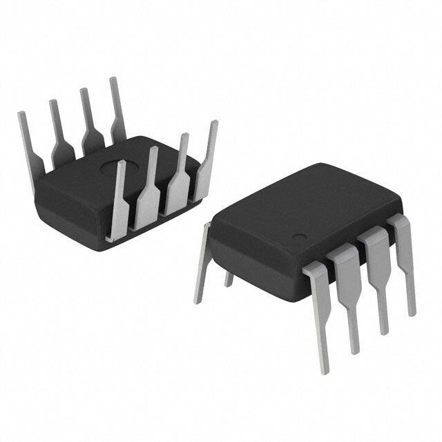
| 供应商器件封装 | 8-PDIP |
| 共模抑制比—最小值 | 70 dB |
| 关闭 | No Shutdown |
| 其它名称 | 296-17460-5 |
| 包装 | 管件 |
| 单位重量 | 440.400 mg |
| 单电源电压 | 10 V to 30 V |
| 压摆率 | 1.7 V/µs |
| 双重电源电压 | +/- 9 V, +/- 12 V |
| 商标 | Texas Instruments |
| 增益带宽生成 | 3 MHz |
| 增益带宽积 | 3MHz |
| 安装类型 | 通孔 |
| 安装风格 | Through Hole |
| 封装 | Tube |
| 封装/外壳 | 8-DIP(0.300",7.62mm) |
| 封装/箱体 | PDIP-8 |
| 工作温度 | -40°C ~ 85°C |
| 工作电源电压 | 10 V to 30 V, +/- 5 V to +/- 15 V |
| 工厂包装数量 | 50 |
| 技术 | Bipolar |
| 放大器类型 | 通用 |
| 最大双重电源电压 | +/- 15 V |
| 最大工作温度 | + 85 C |
| 最小双重电源电压 | +/- 5 V |
| 最小工作温度 | - 40 C |
| 标准包装 | 50 |
| 电压-电源,单/双 (±) | 10 V ~ 30 V, ±5 V ~ 15 V |
| 电压-输入失调 | 500µV |
| 电流-电源 | 2.5mA |
| 电流-输入偏置 | 150nA |
| 电流-输出/通道 | - |
| 电源电流 | 5.6 mA |
| 电路数 | 2 |
| 系列 | RC4558 |
| 转换速度 | 1.7 V/us |
| 输入偏压电流—最大 | 500 nA |
| 输入参考电压噪声 | 8 nV |
| 输入补偿电压 | 6 mV |
| 输出类型 | - |
| 通道数量 | 2 Channel |


PDF Datasheet 数据手册内容提取
Product Sample & Technical Tools & Support & Folder Buy Documents Software Community RC4558 SLOS073G–MARCH1976–REVISEDOCTOBER2014 RC4558 Dual General-Purpose Operational Amplifier 1 Features 3 Description • ContinuousShort-CircuitProtection The RC4558 device is a dual general-purpose 1 operational amplifier, with each half electrically similar • WideCommon-ModeandDifferentialVoltage to the μA741, except that offset null capability is not Ranges provided. • NoFrequencyCompensationRequired The high common-mode input voltage range and the • LowPowerConsumption absence of latch-up make this amplifier ideal for • NoLatch-Up voltage-follower applications. The device is short- circuit protected, and the internal frequency • Unity-GainBandwidth:3MHzTyp compensation ensures stability without external • GainandPhaseMatchBetweenAmplifiers components. • LowNoise:8nV/√HzTypat1kHz DeviceInformation(1) 2 Applications PARTNUMBER PACKAGE(PIN) BODYSIZE • DVDRecordersandPlayers SOIC(8) 4.90mm×3.91mm • ProAudioMixers SOIC(8) 3.00mm×3.00mm RC4558 PDIP(8) 9.81mm×6.35mm TSSOP(8) 3.00mm×4.40mm SOP(8) 6.20mm×5.30mm (1) For all available packages, see the orderable addendum at theendofthedatasheet. NoninvertingAmplifierSchematic RIN VIN + VOUT RG RF 1 An IMPORTANT NOTICE at the end of this data sheet addresses availability, warranty, changes, use in safety-critical applications, intellectualpropertymattersandotherimportantdisclaimers.PRODUCTIONDATA.
RC4558 SLOS073G–MARCH1976–REVISEDOCTOBER2014 www.ti.com Table of Contents 1 Features.................................................................. 1 7.2 FunctionalBlockDiagram.........................................9 2 Applications........................................................... 1 7.3 FeatureDescription...................................................9 3 Description............................................................. 1 7.4 DeviceFunctionalModes..........................................9 4 RevisionHistory..................................................... 2 8 ApplicationandImplementation........................ 10 8.1 TypicalApplication .................................................10 5 PinConfigurationandFunctions......................... 3 9 PowerSupplyRecommendations...................... 13 6 Specifications......................................................... 4 10 Layout................................................................... 14 6.1 AbsoluteMaximumRatings .....................................4 6.2 HandlingRatings.......................................................4 10.1 LayoutGuidelines.................................................14 6.3 RecommendedOperatingConditions.......................4 10.2 LayoutExample....................................................14 6.4 ThermalInformation..................................................4 11 DeviceandDocumentationSupport................. 15 6.5 ElectricalCharacteristics...........................................5 11.1 Trademarks...........................................................15 6.6 OperatingCharacteristics..........................................5 11.2 ElectrostaticDischargeCaution............................15 6.7 TypicalCharacteristics..............................................6 11.3 Glossary................................................................15 7 DetailedDescription.............................................. 9 12 Mechanical,Packaging,andOrderable Information........................................................... 15 7.1 Overview...................................................................9 4 Revision History ChangesfromRevisionF(September2010)toRevisionG Page • AddedApplications,DeviceInformationtable,HandlingRatingstable,FeatureDescriptionsection,Device FunctionalModes,ApplicationandImplementationsection,PowerSupplyRecommendationssection,Layout section,DeviceandDocumentationSupportsection,andMechanical,Packaging,andOrderableInformationsection......1 • RemovedOrderingInformationtable..................................................................................................................................... 1 2 SubmitDocumentationFeedback Copyright©1976–2014,TexasInstrumentsIncorporated ProductFolderLinks:RC4558
RC4558 www.ti.com SLOS073G–MARCH1976–REVISEDOCTOBER2014 5 Pin Configuration and Functions D,DGK,P,PS,OR PWPACKAGE (TOPVIEW) 1OUT 1 8 V + CC 1IN− 2 7 2OUT 1IN+ 3 6 2IN− VCC− 4 5 2IN+ PinFunctions PIN TYPE DESCRIPTION NAME NO. 1IN+ 3 I Noninvertinginput 1IN- 2 I InvertingInput 1OUT 1 O Output 2IN+ 5 I Noninvertinginput 2IN- 6 I InvertingInput 2OUT 7 O Output V + 8 — PositiveSupply CC V - 4 — NegativeSupply CC Copyright©1976–2014,TexasInstrumentsIncorporated SubmitDocumentationFeedback 3 ProductFolderLinks:RC4558
RC4558 SLOS073G–MARCH1976–REVISEDOCTOBER2014 www.ti.com 6 Specifications 6.1 Absolute Maximum Ratings overoperatingfree-airtemperaturerange(unlessotherwisenoted)(1) MIN MAX UNIT V 18 CC+ Supplyvoltage(2) V V –18 CC– V Differentialinputvoltage(3) ±30 V ID V Inputvoltage(anyinput)(2)(4) ±15 V I Durationofoutputshortcircuittoground,oneamplifieratatime(5) Unlimited T Operatingvirtualjunctiontemperature 150 °C J (1) StressesbeyondthoselistedunderAbsoluteMaximumRatingsmaycausepermanentdamagetothedevice.Thesearestressratings only,andfunctionaloperationofthedeviceattheseoranyotherconditionsbeyondthoseindicatedunderRecommendedOperating Conditionsisnotimplied.Exposuretoabsolute-maximum-ratedconditionsforextendedperiodsmayaffectdevicereliability. (2) Allvoltagevalues,unlessotherwisenoted,arewithrespecttothemidpointbetweenV andV . CC+ CC– (3) DifferentialvoltagesareatIN+withrespecttoIN–. (4) Themagnitudeoftheinputvoltagemustneverexceedthemagnitudeofthesupplyvoltageor15V,whicheverisless. (5) Temperatureand/orsupplyvoltagesmustbelimitedtoensurethatthedissipationratingisnotexceeded. 6.2 Handling Ratings MIN MAX UNIT T Storagetemperaturerange -65 150 °C stg Humanbodymodel(HBM),perAECQ100-002(1) 0 500 V Electrostaticdischarge V (ESD) Chargeddevicemodel(CDM),perAECQ100-011 (2) 0 1000 (1) JEDECdocumentJEP155statesthat500-VHBMallowssafemanufacturingwithastandardESDcontrolprocess. (2) JEDECdocumentJEP157statesthat250-VCDMallowssafemanufacturingwithastandardESDcontrolprocess. 6.3 Recommended Operating Conditions MIN MAX UNIT V 5 15 CC+ Supplyvoltage V V –5 –15 CC– RC4558 0 70 T Operatingfree-airtemperature °C A RC4558I –40 85 6.4 Thermal Information RC4558 THERMALMETRIC(1) D DGK P PS PW UNIT 8PINS R Junction-to-ambientthermalresistance 97 172 85 95 149 °C/W θJA (1) Formoreinformationabouttraditionalandnewthermalmetrics,seetheICPackageThermalMetricsapplicationreport,SPRA953. 4 SubmitDocumentationFeedback Copyright©1976–2014,TexasInstrumentsIncorporated ProductFolderLinks:RC4558
RC4558 www.ti.com SLOS073G–MARCH1976–REVISEDOCTOBER2014 6.5 Electrical Characteristics atspecifiedfree-airtemperature,V =15V,V =–15V CC+ CC– PARAMETER CONDTIETSIOTNS(1) TA (2) MIN TYP MAX UNIT 25°C 0.5 6 V Inputoffsetvoltage V =0 mV IO O Fullrange 7.5 25°C 5 200 I Inputoffsetcurrent V =0 nA IO O Fullrange 300 25°C 150 500 I Inputbiascurrent V =0 nA IB O Fullrange 800 V Common-modeinputvoltagerange 25°C ±12 ±14 V ICR R =10kΩ 25°C ±12 ±14 L V Maximumoutputvoltageswing 25°C ±10 ±13 V OM R =2kΩ L Fullrange ±10 R ≥2kΩ, 25°C 20 300 A Large-signaldifferentialvoltageamplification L V/mV VD VO=±10V Fullrange 15 B Unity-gainbandwidth 25°C 3 MHz 1 r Inputresistance 25°C 0.3 5 MΩ i CMRR Common-moderejectionratio 25°C 70 90 dB V =±15V k Supply-voltagesensitivity(ΔV /ΔV ) CC 25°C 30 150 μV/V SVS IO CC to±9V A =100, VD R =100Ω, V Equivalentinputnoisevoltage(closedloop) S 25°C 8 nV/√Hz n f=1kHz, BW=1Hz 25°C 2.5 5.6 V =0, I Supplycurrent(bothamplifiers) O T min 3 6.6 mA CC Noload A T max 2.3 5 A 25°C 75 170 V =0, P Totalpowerdissipation(bothamplifiers) O T min 90 200 mW D Noload A T max 70 150 A Openloop R =1kΩ, 85 V /V Crosstalkattenuation S 25°C dB O1 O2 A =100 f=10kHz 105 VD (1) Allcharacteristicsaremeasuredunderopen-loopconditionswithzerocommon-modeinputvoltage,unlessotherwisespecified. (2) Fullrangeis0°Cto70°CforRC4558and–40°Cto85°CforRC4558I. 6.6 Operating Characteristics V =15V,V =–15V,T =25°C CC+ CC– A PARAMETER TESTCONDITIONS MIN TYP MAX UNIT t Risetime V =20mV, R =2kΩ, C =100pF 0.13 ns r I L L Overshoot V =20mV, R =2kΩ, C =100pF 5% I L L SR Slewrateatunitygain V =10V, R =2kΩ, C =100pF 1.1 1.7 V/μs I L L Copyright©1976–2014,TexasInstrumentsIncorporated SubmitDocumentationFeedback 5 ProductFolderLinks:RC4558
RC4558 SLOS073G–MARCH1976–REVISEDOCTOBER2014 www.ti.com 6.7 Typical Characteristics 6 6 5 5 A A m m – 4 – 4 Current 3 Current 3 Supply 2 Supply 2 – – ICC ICC 1 1 0 0 0 2 4 6 8 10 12 14 16 18 20 -55 -35 -15 5 25 45 65 85 105 125 VCC–SupplyVoltage–V TA–Temperature–°C Figure1.SupplyCurrentvsSupplyVoltage Figure2.SupplyCurrentvsTemperature (TA=25°C) (VCC=±15V) 40 0 40 0 -20 -20 30 30 -40 -40 -60 -60 20 20 dB Gain -80 deg dB Gain -80 deg Gain– 100 Phase --112000 Phase– Gain– 100 Phase --112000 Phase– -140 -140 -160 -160 -10 -10 -180 -180 -20 -200 -20 -200 100 1000 10000 100 1000 10000 f–Frequency–kHz f–Frequency–kHz Figure3.GainandPhasevsFrequency Figure4.GainandPhasevsFrequency (V =±15V,R =2kΩ,C =22pF) (V =±15V,R =10kΩ,C =22pF) CC L L CC L L 15 30 10 25 V V Swing– 5 Swing– 20 Voltage 0 Voltage 15 Output -5 Output 10 – – VOM -10 VOM 5 -15 0 6 8 10 12 14 16 18 1.E1+00 1.E1+001 1.E10+002 1.E1+k03 1.1E0+k04 11.E0+00k5 1.1EM+06 VCC–SupplyVoltage–V f–Frequency–Hz Figure5.OutputVoltageSwingvsSupplyVoltage Figure6.OutputVoltageSwingvsFrequency (RL=2kΩ,TA=25°C) (VCC=±15V,RL=2kΩ,TA=25°C) 6 SubmitDocumentationFeedback Copyright©1976–2014,TexasInstrumentsIncorporated ProductFolderLinks:RC4558
RC4558 www.ti.com SLOS073G–MARCH1976–REVISEDOCTOBER2014 Typical Characteristics (continued) 32 15 30 14.75 V 28 V – – 14.5 VoltageSwing 222246 VoltageSwing 14.1245 utput 20 utput 13.75 O 18 O – – 13.5 VOM 16 VOM 13.25 14 12 13 100 1000 10000 -55 -35 -15 5 25 45 65 85 105 125 RloaRd–L–L LooaaddR Reessisistatannccee– –W TA–Temperature–°C Figure7.OutputVoltageSwingvsLoadResistance Figure8.OutputVoltageSwingvsTemperature (VCC=±15V,TA=25°C) (VCC=±15V,RL=10kΩ) -12 120 110 -12.25 100 V ng– -12.5 dB 90 geSwi -12.75 Gain– 7800 Volta -13 Loop 60 Output -13.25 –Open 4500 –OM -13.5 GM 30 V – 20 -13.75 10 -14 0 -55 -35 -15 5 25 45 65 85 105 125 11.E0+002 11.Ek+03 11.E0+k04 1.1E0+00k5 1.E1+M06 1.1E0+M07 TA–Temperature–°C f–Frequency–Hz Figure9.NegativeOutputVoltageSwingvsTemperature Figure10.OpenLoopGainvsFrequency (V =±15V,R =10kΩ) (V =±15V,R =2kΩ,C =22pF,T =25°C) CC L CC L L A 200 0.003 190 0.002 180 A V urrent–n 116700 Voltage– 0.001 –InputBiasC 111345000 –InputOffset -0.0010 IIB 120 VIO -0.002 110 100 -0.003 -55 -35 -15 5 25 45 65 85 105 125 -55 -35 -15 5 25 45 65 85 105 125 TA–Temperature–°C TA–Temperature–°C Figure11.InputBiasCurrentvsTemperature Figure12.InputOffsetVoltagevsTemperature (V =±15V) (V =±15V) CC CC Copyright©1976–2014,TexasInstrumentsIncorporated SubmitDocumentationFeedback 7 ProductFolderLinks:RC4558
RC4558 SLOS073G–MARCH1976–REVISEDOCTOBER2014 www.ti.com Typical Characteristics (continued) 14 12 HzHz) ÖVoltage – nV/oltage–nV/rt( 180 eV Noisoise 6 V– Input –InputNn 4 Vn 2 0 1.E1+001 1.1E0+002 1.E1+k03 1.E1+00k4 1.1E0+00k5 f–Frequency–Hz Figure13.InputNoiseVoltagevsFrequency (V =±15V,T =25°C) CC A 8 SubmitDocumentationFeedback Copyright©1976–2014,TexasInstrumentsIncorporated ProductFolderLinks:RC4558
RC4558 www.ti.com SLOS073G–MARCH1976–REVISEDOCTOBER2014 7 Detailed Description 7.1 Overview The RC4558 device is a dual general-purpose operational amplifier, with each half electrically similar to the μA741,exceptthatoffsetnullcapabilityisnotprovided. The high common-mode input voltage range and the absence of latch-up make this amplifier ideal for voltage- follower applications. The device is short-circuit protected, and the internal frequency compensation ensures stabilitywithoutexternalcomponents. 7.2 Functional Block Diagram VCC+ IN− IN+ OUT VCC− 7.3 Feature Description 7.3.1 Unity-GainBandwidth The unity-gain bandwidth is the frequency up to which an amplifier with a unity gain may be operated without greatlydistortingthesignal.TheRC4558devicehasa3-MHzunity-gainbandwidth. 7.3.2 Common-ModeRejectionRatio The common-mode rejection ratio (CMRR) of an amplifier is a measure of how well the device rejects unwanted input signals common to both input leads. It is found by taking the ratio of the change in input offset voltage to the change in the input voltage, then converting to decibels. Ideally the CMRR is infinite, but in practice, amplifiersaredesignedtohaveitashighaspossible.TheCMRRoftheRC4558deviceis90dB. 7.3.3 SlewRate The slew rate is the rate at which an operational amplifier can change its output when there is a change on the input.TheRC4558devicehasa1.7V/μsslewrate. 7.4 Device Functional Modes The RC4558 device is powered on when the supply is connected. Each of these devices can be operated as a singlesupplyoperationalamplifierordualsupplyamplifierdependingontheapplication. Copyright©1976–2014,TexasInstrumentsIncorporated SubmitDocumentationFeedback 9 ProductFolderLinks:RC4558
RC4558 SLOS073G–MARCH1976–REVISEDOCTOBER2014 www.ti.com 8 Application and Implementation NOTE Information in the following applications sections is not part of the TI component specification, and TI does not warrant its accuracy or completeness. TI’s customers are responsible for determining suitability of components for their purposes. Customers should validateandtesttheirdesignimplementationtoconfirmsystemfunctionality. 8.1 Typical Application Some applications require differential signals. Figure 14 shows a simple circuit to convert a single-ended input of 2 V to 10 V into differential output of ±8 V on a single 15-V supply. The output range is intentionally limited to maximize linearity. The circuit is composed of two amplifiers. One amplifier acts as a buffer and creates a voltage, V . The second amplifier inverts the input and adds a reference voltage to generate V . Both OUT+ OUT– V andV rangefrom2Vto10V.Thedifference,V ,isthedifferencebetweenV andV . OUT+ OUT– DIFF OUT+ OUT– R 2 15 V R 1 V OUT- + R + 3 V REF R 12 V 4 V DIFF ± V OUT+ + V IN Figure14. SchematicforSingle-EndedInputtoDifferentialOutputConversion 10 SubmitDocumentationFeedback Copyright©1976–2014,TexasInstrumentsIncorporated ProductFolderLinks:RC4558
RC4558 www.ti.com SLOS073G–MARCH1976–REVISEDOCTOBER2014 Typical Application (continued) 8.1.1 DesignRequirements Thedesignrequirementsareasfollows: • Supplyvoltage:15V • Referencevoltage:12V • Input:2Vto10V • Outputdifferential: ±8V 8.1.2 DetailedDesignProcedure The circuit in Figure 14 takes a single-ended input signal, V , and generates two output signals, V and IN OUT+ V using two amplifiers and a reference voltage, V . V is the output of the first amplifier and is a OUT– REF OUT+ buffered version of the input signal, V (see Equation 1). V is the output of the second amplifier which uses IN OUT– V to add an offset voltage to V and feedback to add inverting gain. The transfer function for V is REF IN OUT– Equation2. V =V (1) OUT+ IN æ R4 ö æ R2ö R2 VOoUuTt-= VRreEFf´çèR33++4R44÷ø´çè1+ R211÷ø-VIiNn´R121 (2) The differential output signal, V , is the difference between the two single-ended output signals, V and DIFF OUT+ V . Equation 3 shows the transfer function for V . By applying the conditions that R = R and R = R , the OUT– DIFF 1 2 3 4 transfer function is simplified into Equation 6. Using this configuration, the maximum input signal is equal to the reference voltage and the maximum output of each amplifier is equal to the V . The differential output range is REF 2×V .Furthermore,thecommonmodevoltagewillbeonehalfofV (seeEquation7). REF REF æ R ö æ R öæ R ö VDIFF = VOUT+ -VOUT- = VIN ´ çè1 + R21 ÷ø - VREF ´ çèR3 +4R4 ÷øçè1 + R21 ÷ø (3) V =V (4) OUT+ IN V =V –V (5) OUT– REF IN V =2×V –V (6) DIFF IN REF æV + V ö 1 Vcm =çè OUT+ 2 OUT- ÷ø = 2VREF (7) 8.1.2.1 AmplifierSelection Linearity over the input range is key for good dc accuracy. The common mode input range and the output swing limitations determine the linearity. In general, an amplifier with rail-to-rail input and output swing is required. Bandwidth is a key concern for this design. Because RC4558 has a bandwidth of 3 MHz, this circuit will only be abletoprocesssignalswithfrequenciesoflessthan3MHz. 8.1.2.2 PassiveComponentSelection Because the transfer function of V is heavily reliant on resistors (R , R , R , and R ), use resistors with low OUT– 1 2 3 4 tolerances to maximize performance and minimize error. This design used resistors with resistance values of 36 kΩ with tolerances measured to be within 2%. But, if the noise of the system is a key parameter, the user can selectsmallerresistancevalues(6kΩorlower)tokeeptheoverallsystemnoiselow.Thisensuresthatthenoise fromtheresistorsislowerthantheamplifiernoise. Copyright©1976–2014,TexasInstrumentsIncorporated SubmitDocumentationFeedback 11 ProductFolderLinks:RC4558
RC4558 SLOS073G–MARCH1976–REVISEDOCTOBER2014 www.ti.com Typical Application (continued) 8.1.3 ApplicationCurves The measured transfer functions in Figure 15, Figure 16, and Figure 17 were generated by sweeping the input voltagefrom0Vto12V.However,thisdesignshouldonlybeusedbetween2Vand10Vforoptimumlinearity. 16 16 12 14 12 8 DIFF (V) 04 OUT+ (V) 108 V V 6 ±4 4 ±8 2 ±12 0 0 2 4 6 8 10 12 0 2 4 6 8 10 12 VIN (V) VIN (V) C003 C001 Figure15.DifferentialOutputVoltageNodevsInput Figure16.PositiveOutputVoltageNodevsInputVoltage Voltage 12 10 8 V) tT ( 6 U O V 4 2 0 0 2 4 6 8 10 12 VIN (V) C002 Figure17.PositiveOutputVoltageNodevsInputVoltage 12 SubmitDocumentationFeedback Copyright©1976–2014,TexasInstrumentsIncorporated ProductFolderLinks:RC4558
RC4558 www.ti.com SLOS073G–MARCH1976–REVISEDOCTOBER2014 9 Power Supply Recommendations The RC4558 device is specified for operation from ±5 V to ±15 V; many specifications apply from –0°C to 70°C. The Typical Characteristics section presents parameters that can exhibit significant variance with regard to operatingvoltageortemperature. CAUTION Supply voltages outside of the ±18-V range can permanently damage the device (see theAbsoluteMaximumRatings). Place 0.1-μF bypass capacitors close to the power-supply pins to reduce errors coupling in from noisy or high impedance power supplies. For more detailed information on bypass capacitor placement, refer to the Layout Guidelines. Copyright©1976–2014,TexasInstrumentsIncorporated SubmitDocumentationFeedback 13 ProductFolderLinks:RC4558
RC4558 SLOS073G–MARCH1976–REVISEDOCTOBER2014 www.ti.com 10 Layout 10.1 Layout Guidelines Forbestoperationalperformanceofthedevice,usegoodPCBlayoutpractices,including: • Noise can propagate into analog circuitry through the power pins of the circuit as a whole and the operational amplifier. Bypass capacitors are used to reduce the coupled noise by providing low impedance power sourceslocaltotheanalogcircuitry. – Connect low-ESR, 0.1-μF ceramic bypass capacitors between each supply pin and ground, placed as close to the device as possible. A single bypass capacitor from V+ to ground is applicable for single supplyapplications. • Separate grounding for analog and digital portions of circuitry is one of the simplest and most-effective methods of noise suppression. One or more layers on multilayer PCBs are usually devoted to ground planes. A ground plane helps distribute heat and reduces EMI noise pickup. Make sure to physically separate digital and analog grounds, paying attention to the flow of the ground current. For more detailed information, refer to CircuitBoardLayoutTechniques,(SLOA089). • To reduce parasitic coupling, run the input traces as far away from the supply or output traces as possible. If it is not possible to keep them separate, it is much better to cross the sensitive trace perpendicular as opposedtoinparallelwiththenoisytrace. • Place the external components as close to the device as possible. Keeping RF and RG close to the inverting inputminimizesparasiticcapacitance,asshowninLayoutExample. • Keep the length of input traces as short as possible. Always remember that the input traces are the most sensitivepartofthecircuit. • Consider a driven, low-impedance guard ring around the critical traces. A guard ring can significantly reduce leakagecurrentsfromnearbytracesthatareatdifferentpotentials. 10.2 Layout Example RIN VIN + VOUT RG RF Figure18. OperationalAmplifierSchematicforNoninvertingConfiguration Place components close to device and to each other to reduce parasitic errors Run the input traces as far VS+ away from the supply lines as possible RF OUT1 VCC+ RG GND IN1í OUT2 VIN IN1+ IN2í GND RIN VCCí IN2+ Only needed for Use low-ESR, ceramic dual-supply bypass capacitor operation GND VS- (or GND for single supply) Ground (GND) plane on another layer Figure19. OperationalAmplifierBoardLayoutforNoninvertingConfiguration 14 SubmitDocumentationFeedback Copyright©1976–2014,TexasInstrumentsIncorporated ProductFolderLinks:RC4558
RC4558 www.ti.com SLOS073G–MARCH1976–REVISEDOCTOBER2014 11 Device and Documentation Support 11.1 Trademarks Alltrademarksarethepropertyoftheirrespectiveowners. 11.2 Electrostatic Discharge Caution This integrated circuit can be damaged by ESD. Texas Instruments recommends that all integrated circuits be handled with appropriateprecautions.Failuretoobserveproperhandlingandinstallationprocedurescancausedamage. ESDdamagecanrangefromsubtleperformancedegradationtocompletedevicefailure.Precisionintegratedcircuitsmaybemore susceptibletodamagebecauseverysmallparametricchangescouldcausethedevicenottomeetitspublishedspecifications. 11.3 Glossary SLYZ022—TIGlossary. Thisglossarylistsandexplainsterms,acronymsanddefinitions. 12 Mechanical, Packaging, and Orderable Information The following pages include mechanical packaging and orderable information. This information is the most current data available for the designated devices. This data is subject to change without notice and revision of thisdocument.Forbrowserbasedversionsofthisdatasheet,refertothelefthandnavigation. Copyright©1976–2014,TexasInstrumentsIncorporated SubmitDocumentationFeedback 15 ProductFolderLinks:RC4558
PACKAGE OPTION ADDENDUM www.ti.com 6-Feb-2020 PACKAGING INFORMATION Orderable Device Status Package Type Package Pins Package Eco Plan Lead/Ball Finish MSL Peak Temp Op Temp (°C) Device Marking Samples (1) Drawing Qty (2) (6) (3) (4/5) RC4558D ACTIVE SOIC D 8 75 Green (RoHS NIPDAU Level-1-260C-UNLIM 0 to 70 RC4558 & no Sb/Br) RC4558DE4 ACTIVE SOIC D 8 75 Green (RoHS NIPDAU Level-1-260C-UNLIM 0 to 70 RC4558 & no Sb/Br) RC4558DGKR ACTIVE VSSOP DGK 8 2500 Green (RoHS NIPDAU | NIPDAUAG Level-1-260C-UNLIM 0 to 70 (YRP, YRS, YRU) & no Sb/Br) RC4558DGKRG4 ACTIVE VSSOP DGK 8 2500 Green (RoHS NIPDAUAG Level-1-260C-UNLIM 0 to 70 (YRP, YRS, YRU) & no Sb/Br) RC4558DR ACTIVE SOIC D 8 2500 Green (RoHS NIPDAU | SN Level-1-260C-UNLIM 0 to 70 RC4558 & no Sb/Br) RC4558DRG3 ACTIVE SOIC D 8 2500 Green (RoHS SN Level-1-260C-UNLIM 0 to 70 RC4558 & no Sb/Br) RC4558DRG4 ACTIVE SOIC D 8 2500 Green (RoHS NIPDAU Level-1-260C-UNLIM 0 to 70 RC4558 & no Sb/Br) RC4558ID ACTIVE SOIC D 8 75 Green (RoHS NIPDAU Level-1-260C-UNLIM -40 to 85 R4558I & no Sb/Br) RC4558IDGKR ACTIVE VSSOP DGK 8 2500 Green (RoHS NIPDAU | NIPDAUAG Level-1-260C-UNLIM -40 to 85 (YSP, YSS, YSU) & no Sb/Br) RC4558IDGKRG4 ACTIVE VSSOP DGK 8 2500 Green (RoHS NIPDAUAG Level-1-260C-UNLIM -40 to 85 (YSP, YSS, YSU) & no Sb/Br) RC4558IDR ACTIVE SOIC D 8 2500 Green (RoHS NIPDAU Level-1-260C-UNLIM -40 to 85 R4558I & no Sb/Br) RC4558IDRG4 ACTIVE SOIC D 8 2500 Green (RoHS NIPDAU Level-1-260C-UNLIM -40 to 85 R4558I & no Sb/Br) RC4558IP ACTIVE PDIP P 8 50 Green (RoHS NIPDAU N / A for Pkg Type -40 to 85 RC4558IP & no Sb/Br) RC4558IPW ACTIVE TSSOP PW 8 150 Green (RoHS NIPDAU Level-1-260C-UNLIM -40 to 85 R4558I & no Sb/Br) RC4558IPWR ACTIVE TSSOP PW 8 2000 Green (RoHS NIPDAU | SN Level-1-260C-UNLIM -40 to 85 R4558I & no Sb/Br) RC4558P ACTIVE PDIP P 8 50 Green (RoHS NIPDAU N / A for Pkg Type 0 to 70 RC4558P & no Sb/Br) RC4558PE4 ACTIVE PDIP P 8 50 Green (RoHS NIPDAU N / A for Pkg Type 0 to 70 RC4558P & no Sb/Br) Addendum-Page 1
PACKAGE OPTION ADDENDUM www.ti.com 6-Feb-2020 Orderable Device Status Package Type Package Pins Package Eco Plan Lead/Ball Finish MSL Peak Temp Op Temp (°C) Device Marking Samples (1) Drawing Qty (2) (6) (3) (4/5) RC4558PSR ACTIVE SO PS 8 2000 Green (RoHS NIPDAU Level-1-260C-UNLIM 0 to 70 R4558 & no Sb/Br) RC4558PSRG4 ACTIVE SO PS 8 2000 Green (RoHS NIPDAU Level-1-260C-UNLIM 0 to 70 R4558 & no Sb/Br) RC4558PW ACTIVE TSSOP PW 8 150 Green (RoHS NIPDAU Level-1-260C-UNLIM 0 to 70 R4558 & no Sb/Br) RC4558PWR ACTIVE TSSOP PW 8 2000 Green (RoHS NIPDAU | SN Level-1-260C-UNLIM 0 to 70 R4558 & no Sb/Br) (1) The marketing status values are defined as follows: ACTIVE: Product device recommended for new designs. LIFEBUY: TI has announced that the device will be discontinued, and a lifetime-buy period is in effect. NRND: Not recommended for new designs. Device is in production to support existing customers, but TI does not recommend using this part in a new design. PREVIEW: Device has been announced but is not in production. Samples may or may not be available. OBSOLETE: TI has discontinued the production of the device. (2) RoHS: TI defines "RoHS" to mean semiconductor products that are compliant with the current EU RoHS requirements for all 10 RoHS substances, including the requirement that RoHS substance do not exceed 0.1% by weight in homogeneous materials. Where designed to be soldered at high temperatures, "RoHS" products are suitable for use in specified lead-free processes. TI may reference these types of products as "Pb-Free". RoHS Exempt: TI defines "RoHS Exempt" to mean products that contain lead but are compliant with EU RoHS pursuant to a specific EU RoHS exemption. Green: TI defines "Green" to mean the content of Chlorine (Cl) and Bromine (Br) based flame retardants meet JS709B low halogen requirements of <=1000ppm threshold. Antimony trioxide based flame retardants must also meet the <=1000ppm threshold requirement. (3) MSL, Peak Temp. - The Moisture Sensitivity Level rating according to the JEDEC industry standard classifications, and peak solder temperature. (4) There may be additional marking, which relates to the logo, the lot trace code information, or the environmental category on the device. (5) Multiple Device Markings will be inside parentheses. Only one Device Marking contained in parentheses and separated by a "~" will appear on a device. If a line is indented then it is a continuation of the previous line and the two combined represent the entire Device Marking for that device. (6) Lead/Ball Finish - Orderable Devices may have multiple material finish options. Finish options are separated by a vertical ruled line. Lead/Ball Finish values may wrap to two lines if the finish value exceeds the maximum column width. Important Information and Disclaimer:The information provided on this page represents TI's knowledge and belief as of the date that it is provided. TI bases its knowledge and belief on information provided by third parties, and makes no representation or warranty as to the accuracy of such information. Efforts are underway to better integrate information from third parties. TI has taken and continues to take reasonable steps to provide representative and accurate information but may not have conducted destructive testing or chemical analysis on incoming materials and chemicals. TI and TI suppliers consider certain information to be proprietary, and thus CAS numbers and other limited information may not be available for release. Addendum-Page 2
PACKAGE OPTION ADDENDUM www.ti.com 6-Feb-2020 In no event shall TI's liability arising out of such information exceed the total purchase price of the TI part(s) at issue in this document sold by TI to Customer on an annual basis. Addendum-Page 3
PACKAGE MATERIALS INFORMATION www.ti.com 28-Dec-2019 TAPE AND REEL INFORMATION *Alldimensionsarenominal Device Package Package Pins SPQ Reel Reel A0 B0 K0 P1 W Pin1 Type Drawing Diameter Width (mm) (mm) (mm) (mm) (mm) Quadrant (mm) W1(mm) RC4558DGKR VSSOP DGK 8 2500 330.0 12.4 5.3 3.4 1.4 8.0 12.0 Q1 RC4558DR SOIC D 8 2500 330.0 12.4 6.4 5.2 2.1 8.0 12.0 Q1 RC4558DR SOIC D 8 2500 330.0 12.8 6.4 5.2 2.1 8.0 12.0 Q1 RC4558DR SOIC D 8 2500 330.0 12.4 6.4 5.2 2.1 8.0 12.0 Q1 RC4558DRG3 SOIC D 8 2500 330.0 12.8 6.4 5.2 2.1 8.0 12.0 Q1 RC4558DRG4 SOIC D 8 2500 330.0 12.4 6.4 5.2 2.1 8.0 12.0 Q1 RC4558DRG4 SOIC D 8 2500 330.0 12.4 6.4 5.2 2.1 8.0 12.0 Q1 RC4558IDGKR VSSOP DGK 8 2500 330.0 12.4 5.3 3.4 1.4 8.0 12.0 Q1 RC4558IDR SOIC D 8 2500 330.0 12.4 6.4 5.2 2.1 8.0 12.0 Q1 RC4558IPWR TSSOP PW 8 2000 330.0 12.4 7.0 3.6 1.6 8.0 12.0 Q1 RC4558IPWR TSSOP PW 8 2000 330.0 12.4 7.0 3.6 1.6 8.0 12.0 Q1 RC4558PWR TSSOP PW 8 2000 330.0 12.4 7.0 3.6 1.6 8.0 12.0 Q1 RC4558PWR TSSOP PW 8 2000 330.0 12.4 7.0 3.6 1.6 8.0 12.0 Q1 PackMaterials-Page1
PACKAGE MATERIALS INFORMATION www.ti.com 28-Dec-2019 *Alldimensionsarenominal Device PackageType PackageDrawing Pins SPQ Length(mm) Width(mm) Height(mm) RC4558DGKR VSSOP DGK 8 2500 364.0 364.0 27.0 RC4558DR SOIC D 8 2500 340.5 338.1 20.6 RC4558DR SOIC D 8 2500 364.0 364.0 27.0 RC4558DR SOIC D 8 2500 367.0 367.0 35.0 RC4558DRG3 SOIC D 8 2500 364.0 364.0 27.0 RC4558DRG4 SOIC D 8 2500 367.0 367.0 35.0 RC4558DRG4 SOIC D 8 2500 340.5 338.1 20.6 RC4558IDGKR VSSOP DGK 8 2500 364.0 364.0 27.0 RC4558IDR SOIC D 8 2500 340.5 338.1 20.6 RC4558IPWR TSSOP PW 8 2000 367.0 367.0 35.0 RC4558IPWR TSSOP PW 8 2000 364.0 364.0 27.0 RC4558PWR TSSOP PW 8 2000 367.0 367.0 35.0 RC4558PWR TSSOP PW 8 2000 364.0 364.0 27.0 PackMaterials-Page2
PACKAGE OUTLINE D0008A SOIC - 1.75 mm max height SCALE 2.800 SMALL OUTLINE INTEGRATED CIRCUIT C SEATING PLANE .228-.244 TYP [5.80-6.19] .004 [0.1] C A PIN 1 ID AREA 6X .050 [1.27] 8 1 2X .189-.197 [4.81-5.00] .150 NOTE 3 [3.81] 4X (0 -15 ) 4 5 8X .012-.020 B .150-.157 [0.31-0.51] .069 MAX [3.81-3.98] .010 [0.25] C A B [1.75] NOTE 4 .005-.010 TYP [0.13-0.25] 4X (0 -15 ) SEE DETAIL A .010 [0.25] .004-.010 0 - 8 [0.11-0.25] .016-.050 [0.41-1.27] DETAIL A (.041) TYPICAL [1.04] 4214825/C 02/2019 NOTES: 1. Linear dimensions are in inches [millimeters]. Dimensions in parenthesis are for reference only. Controlling dimensions are in inches. Dimensioning and tolerancing per ASME Y14.5M. 2. This drawing is subject to change without notice. 3. This dimension does not include mold flash, protrusions, or gate burrs. Mold flash, protrusions, or gate burrs shall not exceed .006 [0.15] per side. 4. This dimension does not include interlead flash. 5. Reference JEDEC registration MS-012, variation AA. www.ti.com
EXAMPLE BOARD LAYOUT D0008A SOIC - 1.75 mm max height SMALL OUTLINE INTEGRATED CIRCUIT 8X (.061 ) [1.55] SYMM SEE DETAILS 1 8 8X (.024) [0.6] SYMM (R.002 ) TYP [0.05] 5 4 6X (.050 ) [1.27] (.213) [5.4] LAND PATTERN EXAMPLE EXPOSED METAL SHOWN SCALE:8X SOLDER MASK SOLDER MASK METAL OPENING OPENING METAL UNDER SOLDER MASK EXPOSED METAL EXPOSED METAL .0028 MAX .0028 MIN [0.07] [0.07] ALL AROUND ALL AROUND NON SOLDER MASK SOLDER MASK DEFINED DEFINED SOLDER MASK DETAILS 4214825/C 02/2019 NOTES: (continued) 6. Publication IPC-7351 may have alternate designs. 7. Solder mask tolerances between and around signal pads can vary based on board fabrication site. www.ti.com
EXAMPLE STENCIL DESIGN D0008A SOIC - 1.75 mm max height SMALL OUTLINE INTEGRATED CIRCUIT 8X (.061 ) [1.55] SYMM 1 8 8X (.024) [0.6] SYMM (R.002 ) TYP [0.05] 5 4 6X (.050 ) [1.27] (.213) [5.4] SOLDER PASTE EXAMPLE BASED ON .005 INCH [0.125 MM] THICK STENCIL SCALE:8X 4214825/C 02/2019 NOTES: (continued) 8. Laser cutting apertures with trapezoidal walls and rounded corners may offer better paste release. IPC-7525 may have alternate design recommendations. 9. Board assembly site may have different recommendations for stencil design. www.ti.com
None
None
None
None
None
PACKAGE OUTLINE PW0008A TSSOP - 1.2 mm max height SCALE 2.800 SMALL OUTLINE PACKAGE C 6.6 TYP SEATING PLANE 6.2 PIN 1 ID A 0.1 C AREA 6X 0.65 8 1 3.1 2X 2.9 NOTE 3 1.95 4 5 0.30 8X 0.19 4.5 1.2 MAX B 0.1 C A B 4.3 NOTE 4 (0.15) TYP SEE DETAIL A 0.25 GAGE PLANE 0.15 0.75 0 - 8 0.05 0.50 DETAIL A TYPICAL 4221848/A 02/2015 NOTES: 1. All linear dimensions are in millimeters. Any dimensions in parenthesis are for reference only. Dimensioning and tolerancing per ASME Y14.5M. 2. This drawing is subject to change without notice. 3. This dimension does not include mold flash, protrusions, or gate burrs. Mold flash, protrusions, or gate burrs shall not exceed 0.15 mm per side. 4. This dimension does not include interlead flash. Interlead flash shall not exceed 0.25 mm per side. 5. Reference JEDEC registration MO-153, variation AA. www.ti.com
EXAMPLE BOARD LAYOUT PW0008A TSSOP - 1.2 mm max height SMALL OUTLINE PACKAGE 8X (1.5) 8X (0.45) SYMM (R0.05) 1 TYP 8 SYMM 6X (0.65) 5 4 (5.8) LAND PATTERN EXAMPLE SCALE:10X SOOPLEDNEINRG MASK METAL MSOELTDAEL RU NMDAESRK SOOPLEDNEINRG MASK 0.05 MAX 0.05 MIN ALL AROUND ALL AROUND NON SOLDER MASK SOLDER MASK DEFINED DEFINED SOLDER MASK DETAILS NOT TO SCALE 4221848/A 02/2015 NOTES: (continued) 6. Publication IPC-7351 may have alternate designs. 7. Solder mask tolerances between and around signal pads can vary based on board fabrication site. www.ti.com
EXAMPLE STENCIL DESIGN PW0008A TSSOP - 1.2 mm max height SMALL OUTLINE PACKAGE 8X (1.5) SYMM (R0.05) TYP 8X (0.45) 1 8 SYMM 6X (0.65) 5 4 (5.8) SOLDER PASTE EXAMPLE BASED ON 0.125 mm THICK STENCIL SCALE:10X 4221848/A 02/2015 NOTES: (continued) 8. Laser cutting apertures with trapezoidal walls and rounded corners may offer better paste release. IPC-7525 may have alternate design recommendations. 9. Board assembly site may have different recommendations for stencil design. www.ti.com
IMPORTANTNOTICEANDDISCLAIMER TI PROVIDES TECHNICAL AND RELIABILITY DATA (INCLUDING DATASHEETS), DESIGN RESOURCES (INCLUDING REFERENCE DESIGNS), APPLICATION OR OTHER DESIGN ADVICE, WEB TOOLS, SAFETY INFORMATION, AND OTHER RESOURCES “AS IS” AND WITH ALL FAULTS, AND DISCLAIMS ALL WARRANTIES, EXPRESS AND IMPLIED, INCLUDING WITHOUT LIMITATION ANY IMPLIED WARRANTIES OF MERCHANTABILITY, FITNESS FOR A PARTICULAR PURPOSE OR NON-INFRINGEMENT OF THIRD PARTY INTELLECTUAL PROPERTY RIGHTS. These resources are intended for skilled developers designing with TI products. You are solely responsible for (1) selecting the appropriate TI products for your application, (2) designing, validating and testing your application, and (3) ensuring your application meets applicable standards, and any other safety, security, or other requirements. These resources are subject to change without notice. TI grants you permission to use these resources only for development of an application that uses the TI products described in the resource. Other reproduction and display of these resources is prohibited. No license is granted to any other TI intellectual property right or to any third party intellectual property right. TI disclaims responsibility for, and you will fully indemnify TI and its representatives against, any claims, damages, costs, losses, and liabilities arising out of your use of these resources. TI’s products are provided subject to TI’s Terms of Sale (www.ti.com/legal/termsofsale.html) or other applicable terms available either on ti.com or provided in conjunction with such TI products. TI’s provision of these resources does not expand or otherwise alter TI’s applicable warranties or warranty disclaimers for TI products. Mailing Address: Texas Instruments, Post Office Box 655303, Dallas, Texas 75265 Copyright © 2020, Texas Instruments Incorporated