ICGOO在线商城 > 传感器,变送器 > 光学传感器 - 反射式 - 模拟输出 > QRE1113
 Datasheet下载
- 型号: QRE1113
- 制造商: Fairchild Semiconductor
- 库位|库存: xxxx|xxxx
- 要求:
| 数量阶梯 | 香港交货 | 国内含税 |
| +xxxx | $xxxx | ¥xxxx |
查看当月历史价格
查看今年历史价格
QRE1113产品简介:
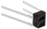
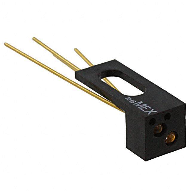
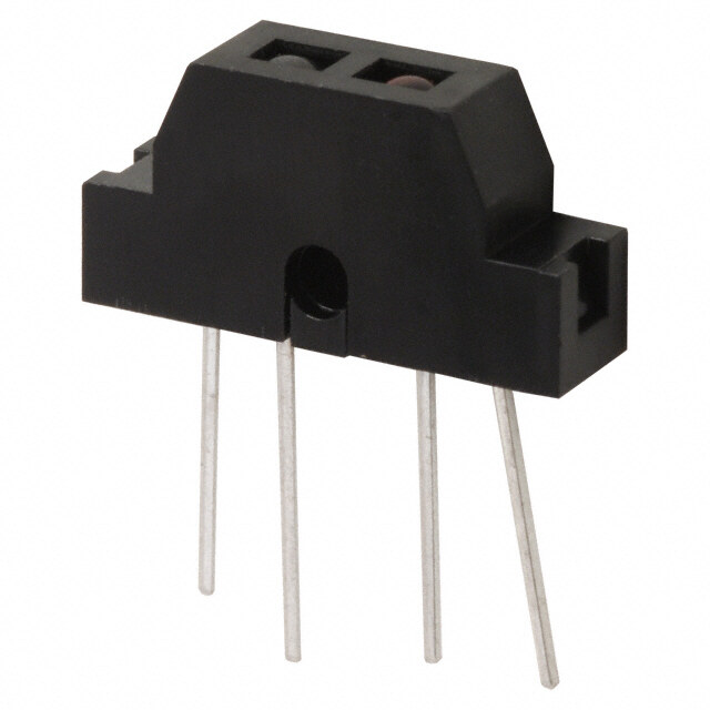
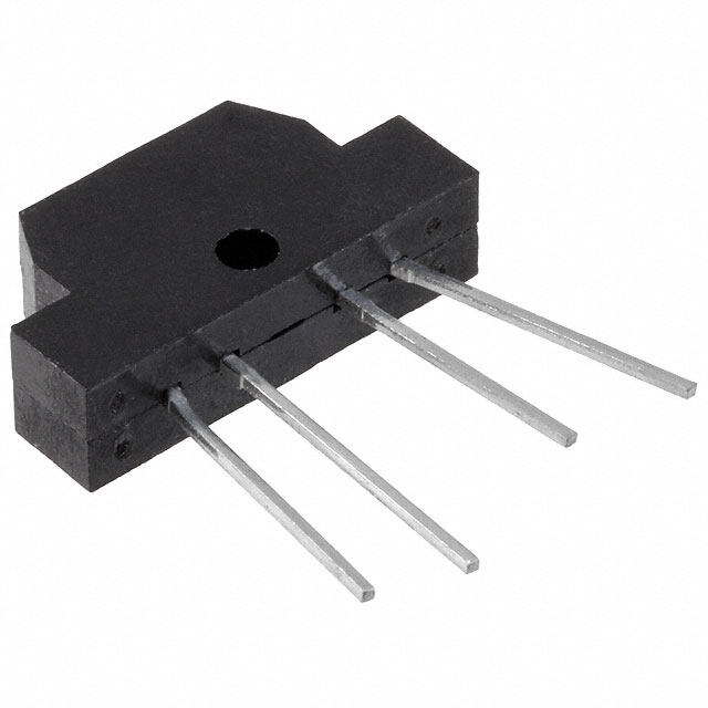
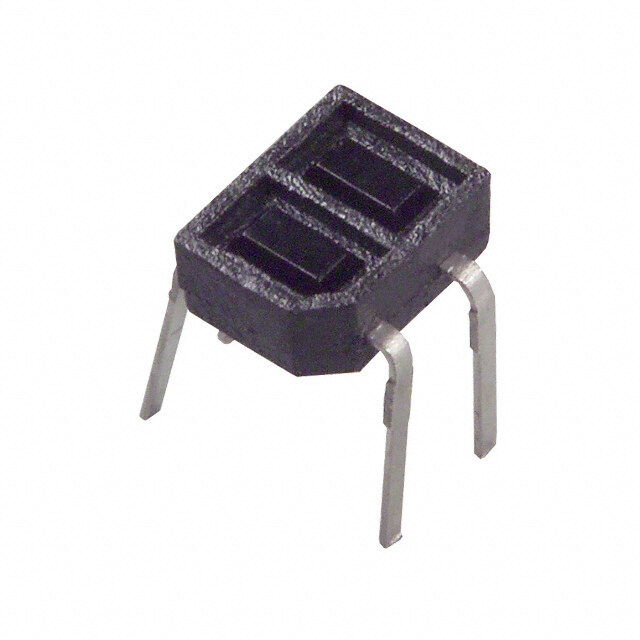
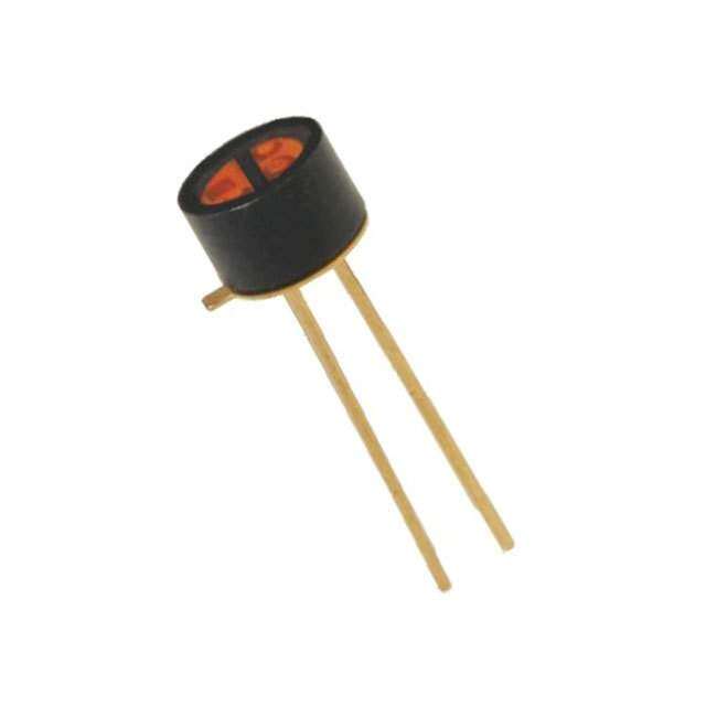
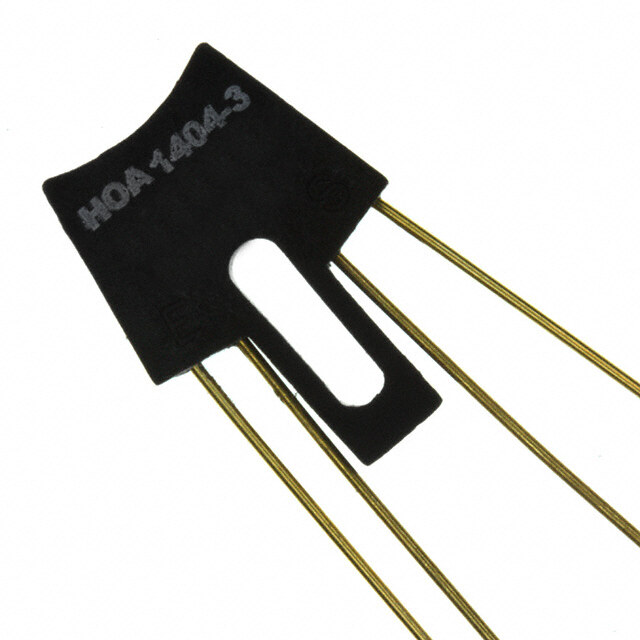
ICGOO电子元器件商城为您提供QRE1113由Fairchild Semiconductor设计生产,在icgoo商城现货销售,并且可以通过原厂、代理商等渠道进行代购。 QRE1113价格参考¥4.38-¥5.58。Fairchild SemiconductorQRE1113封装/规格:光学传感器 - 反射式 - 模拟输出, Reflective Optical Sensor 0.197" (5mm) 4-DIP (0.157", 4.00mm)。您可以下载QRE1113参考资料、Datasheet数据手册功能说明书,资料中有QRE1113 详细功能的应用电路图电压和使用方法及教程。
ON Semiconductor(安森美半导体)的QRE1113是一款光学传感器,属于反射式传感器,并提供模拟输出。该型号的应用场景主要包括以下几个方面:

 1. 物体检测
   QRE1113可以通过检测目标物体对红外光的反射来判断物体是否存在。它适用于需要非接触式检测的小型物体或表面,例如:
   - 自动化生产线中的物品计数。
   - 容器填充液位检测(如检测液体或粉末的高度)。
   - 纸张、塑料或其他材料的边缘检测。

 2. 颜色和表面特性识别
   由于不同颜色或材质对红外光的反射率不同,QRE1113可以用于区分不同的表面特性或颜色。例如:
   - 区分白色和黑色表面(常用于编码器或机器人路径跟踪)。
   - 检测包装材料的颜色变化。

 3. 机器人导航与路径跟踪
   在机器人领域,QRE1113广泛应用于路径跟踪和避障功能。例如:
   - 跟踪黑色引导线:通过检测黑白对比,帮助机器人沿预定路径移动。
   - 避障:检测前方障碍物的存在并触发转向动作。

 4. 速度和位置测量
   QRE1113可用作编码器的一部分,用于测量旋转速度或线性位移。例如:
   - 监控电机转速。
   - 测量传送带的速度或位置。

 5. 消费电子产品
   在一些消费类设备中,QRE1113可用于简单的用户交互或状态监测。例如:
   - 手持设备中的按键检测。
   - 家电中的门开关状态检测。

 6. 医疗与健康设备
   在某些低功耗医疗设备中,QRE1113可用于简单的位置或状态检测。例如:
   - 检测样本容器是否正确放置。
   - 监测运动部件的位置。

 特点总结
QRE1113采用集成设计,包含红外发射二极管和光电晶体管,适合短距离检测(通常为几毫米到几厘米)。其模拟输出允许用户根据具体需求调节灵敏度,适用于多种工业、消费和教育场景。
| 参数 | 数值 |
| 产品目录 | |
| 描述 | SENSOR REFL 5MM PHOTOTRANS THRU光学开关(反射型,光电晶体管输出) Reflective Object Sensor |
| 产品分类 | |
| 品牌 | Fairchild Semiconductor |
| 产品手册 | |
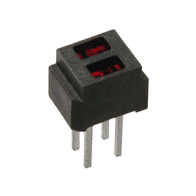
| 产品图片 |
|
| rohs | 符合RoHS无铅 / 符合限制有害物质指令(RoHS)规范要求 |
| 产品系列 | 光学开关(反射型,光电晶体管输出),Fairchild Semiconductor QRE1113- |
| 数据手册 | |
| 产品型号 | QRE1113 |
| 上升时间 | 20 us |
| 下降时间 | 20 us |
| 产品目录绘图 |
|
| 产品目录页面 | |
| 产品种类 | 光学开关(反射型,光电晶体管输出) |
| 包装 | 管件 |
| 单位重量 | 62 mg |
| 反向电压 | 5 V |
| 响应时间 | 20µs, 20µs |
| 商标 | Fairchild Semiconductor |
| 安装类型 | 通孔 |
| 安装风格 | Through Hole |
| 封装 | Tube |
| 封装/外壳 | 4-DIP(0.157",4.00mm) |
| 工作温度 | -40°C ~ 85°C |
| 工厂包装数量 | 160 |
| 感应方式 | Reflective |
| 感应方法 | 反射 |
| 感应距离 | 1 mm |
| 最大工作温度 | + 85 C |
| 最大集电极电流 | 20 mA |
| 最小工作温度 | - 40 C |
| 标准包装 | 160 |
| 正向电压 | 1.2 V |
| 正向电流 | 20 mA |
| 波长 | 940 nm |
| 电压-集射极击穿(最大值) | 30V |
| 电流-DC正向(If) | 50mA |
| 电流-集电极(Ic)(最大值) | 20mA |
| 系列 | QRE1113 |
| 输出类型 | 光电晶体管 |
| 输出设备 | Phototransistor |
| 集电极—发射极最大电压VCEO | 30 V |


- 商务部:美国ITC正式对集成电路等产品启动337调查
- 曝三星4nm工艺存在良率问题 高通将骁龙8 Gen1或转产台积电
- 太阳诱电将投资9.5亿元在常州建新厂生产MLCC 预计2023年完工
- 英特尔发布欧洲新工厂建设计划 深化IDM 2.0 战略
- 台积电先进制程称霸业界 有大客户加持明年业绩稳了
- 达到5530亿美元!SIA预计今年全球半导体销售额将创下新高
- 英特尔拟将自动驾驶子公司Mobileye上市 估值或超500亿美元
- 三星加码芯片和SET,合并消费电子和移动部门,撤换高东真等 CEO
- 三星电子宣布重大人事变动 还合并消费电子和移动部门
- 海关总署:前11个月进口集成电路产品价值2.52万亿元 增长14.8%

PDF Datasheet 数据手册内容提取
Is Now Part of To learn more about ON Semiconductor, please visit our website at www.onsemi.com Please note: As part of the Fairchild Semiconductor integration, some of the Fairchild orderable part numbers will need to change in order to meet ON Semiconductor’s system requirements. Since the ON Semiconductor product management systems do not have the ability to manage part nomenclature that utilizes an underscore (_), the underscore (_) in the Fairchild part numbers will be changed to a dash (-). This document may contain device numbers with an underscore (_). Please check the ON Semiconductor website to verify the updated device numbers. The most current and up-to-date ordering information can be found at www.onsemi.com. Please email any questions regarding the system integration to Fairchild_questions@onsemi.com. ON Semiconductor and the ON Semiconductor logo are trademarks of Semiconductor Components Industries, LLC dba ON Semiconductor or its subsidiaries in the United States and/or other countries. ON Semiconductor owns the rights to a number of patents, trademarks, copyrights, trade secrets, and other intellectual property. A listing of ON Semiconductor’s product/patent coverage may be accessed at www.onsemi.com/site/pdf/Patent-Marking.pdf. ON Semiconductor reserves the right to make changes without further notice to any products herein. ON Semiconductor makes no warranty, representation or guarantee regarding the suitability of its products for any particular purpose, nor does ON Semiconductor assume any liability arising out of the application or use of any product or circuit, and specifically disclaims any and all liability, including without limitation special, consequential or incidental damages. Buyer is responsible for its products and applications using ON Semiconductor products, including compliance with all laws, regulations and safety requirements or standards, regardless of any support or applications information provided by ON Semiconductor. “Typical” parameters which may be provided in ON Semiconductor data sheets and/or specifications can and do vary in different applications and actual performance may vary over time. All operating parameters, including “Typicals” must be validated for each customer application by customer’s technical experts. ON Semiconductor does not convey any license under its patent rights nor the rights of others. ON Semiconductor products are not designed, intended, or authorized for use as a critical component in life support systems or any FDA Class 3 medical devices or medical devices with a same or similar classification in a foreign jurisdiction or any devices intended for implantation in the human body. Should Buyer purchase or use ON Semiconductor products for any such unintended or unauthorized application, Buyer shall indemnify and hold ON Semiconductor and its officers, employees, subsidiaries, affiliates, and distributors harmless against all claims, costs, damages, and expenses, and reasonable attorney fees arising out of, directly or indirectly, any claim of personal injury or death associated with such unintended or unauthorized use, even if such claim alleges that ON Semiconductor was negligent regarding the design or manufacture of the part. ON Semiconductor is an Equal Opportunity/Affirmative Action Employer. This literature is subject to all applicable copyright laws and is not for resale in any manner.
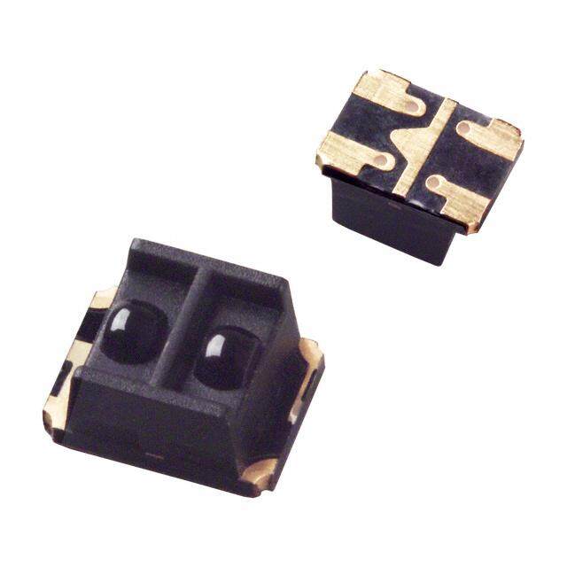
Q R E 1 April 2016 1 1 3 , Q R E QRE1113, QRE1113GR 1 1 1 3 Miniature Reflective Object Sensor G R — M Features i n • Phototransistor Output • Two Leadform Options: Through Hole (QRE1113) ia t • No Contact Surface Sensing SMT Gull Wing (QRE1113GR) u r • Miniature Package • Two Packaging Options: Tube (QRE1113) e R • Lead Form Style: Gull Wing Tape and Reel (QRE1113GR) e f l e c t i QRE1113GR Package Dimensions v e O b j e c (cid:3)(cid:21)(cid:21)(cid:17)(cid:17)(cid:28)(cid:24)(cid:19)(cid:19)(cid:3) t S (cid:19)(cid:17)(cid:25)(cid:19) (cid:3)(cid:20)(cid:17)(cid:19)(cid:19)(cid:3) e (cid:3) (cid:3) n (cid:19)(cid:17)(cid:23)(cid:19) (cid:3)(cid:24)(cid:17)(cid:25)(cid:25)(cid:3) s (cid:23) (cid:22) o (cid:38)(cid:47) (cid:3)(cid:19)(cid:17)(cid:28)(cid:23)(cid:3) r (cid:22)(cid:17)(cid:25)(cid:19) (cid:3)(cid:20)(cid:17)(cid:27)(cid:19)(cid:3) (cid:3)(cid:22)(cid:17)(cid:21)(cid:19)(cid:3) (cid:3)(cid:21)(cid:17)(cid:24)(cid:28)(cid:3) (cid:38)(cid:47) (cid:3)(cid:19)(cid:17)(cid:26)(cid:28)(cid:3) (cid:3)(cid:19)(cid:17)(cid:28)(cid:23)(cid:3) (cid:20) (cid:21) (cid:3)(cid:20)(cid:17)(cid:25)(cid:25)(cid:3) (cid:55)(cid:50)(cid:51)(cid:3)(cid:57)(cid:44)(cid:40)(cid:58) (cid:47)(cid:36)(cid:49)(cid:39)(cid:3)(cid:51)(cid:36)(cid:55)(cid:55)(cid:40)(cid:53)(cid:49)(cid:3)(cid:53)(cid:40)(cid:38)(cid:50)(cid:48)(cid:48)(cid:40)(cid:49)(cid:39)(cid:36)(cid:55)(cid:44)(cid:50)(cid:49) (cid:3)(cid:19)(cid:17)(cid:23)(cid:19)(cid:3) (cid:20)(cid:17)(cid:26)(cid:19) (cid:19)(cid:17)(cid:20)(cid:26) (cid:3) (cid:3) (cid:3) (cid:20)(cid:17)(cid:24)(cid:19) (cid:19)(cid:17)(cid:19)(cid:26) (cid:3)(cid:20)(cid:17)(cid:20)(cid:19)(cid:3) (cid:19)(cid:17)(cid:25)(cid:20)(cid:3)(cid:49)(cid:50)(cid:48)(cid:17)(cid:3)(cid:11)(cid:23)(cid:59)(cid:12) (cid:19)(cid:17)(cid:28)(cid:19) (cid:11)(cid:19)(cid:17)(cid:22)(cid:22)(cid:24)(cid:27)(cid:12)(cid:3)(cid:41)(cid:47)(cid:36)(cid:55)(cid:3)(cid:36)(cid:53)(cid:40)(cid:36) (cid:23)(cid:17)(cid:27)(cid:19) (cid:3) (cid:3) (cid:23)(cid:17)(cid:23)(cid:19) (cid:49)(cid:50)(cid:55)(cid:40)(cid:54)(cid:29) (cid:54)(cid:44)(cid:39)(cid:40)(cid:3)(cid:57)(cid:44)(cid:40)(cid:58) (cid:36)(cid:17)(cid:3)(cid:49)(cid:50)(cid:3)(cid:44)(cid:49)(cid:39)(cid:56)(cid:54)(cid:55)(cid:53)(cid:60)(cid:3)(cid:54)(cid:55)(cid:36)(cid:49)(cid:39)(cid:36)(cid:53)(cid:39)(cid:3)(cid:36)(cid:51)(cid:51)(cid:47)(cid:44)(cid:40)(cid:54) (cid:3)(cid:3)(cid:3)(cid:3)(cid:55)(cid:50)(cid:3)(cid:55)(cid:43)(cid:44)(cid:54)(cid:3)(cid:51)(cid:36)(cid:38)(cid:46)(cid:36)(cid:42)(cid:40) (cid:37)(cid:17)(cid:3)(cid:36)(cid:47)(cid:47)(cid:3)(cid:39)(cid:44)(cid:48)(cid:40)(cid:49)(cid:54)(cid:44)(cid:50)(cid:49)(cid:54)(cid:3)(cid:36)(cid:53)(cid:40)(cid:3)(cid:44)(cid:49)(cid:3)(cid:48)(cid:44)(cid:47)(cid:47)(cid:44)(cid:48)(cid:40)(cid:55)(cid:40)(cid:53)(cid:54) (cid:38)(cid:17)(cid:3)(cid:55)(cid:50)(cid:47)(cid:40)(cid:53)(cid:36)(cid:49)(cid:38)(cid:40)(cid:3)(cid:50)(cid:41)(cid:3) (cid:19)(cid:17)(cid:20)(cid:24)(cid:48)(cid:48)(cid:3)(cid:50)(cid:49)(cid:3)(cid:36)(cid:47)(cid:47)(cid:3) (cid:3)(cid:3)(cid:3)(cid:3)(cid:3)(cid:49)(cid:50)(cid:49)(cid:16)(cid:49)(cid:50)(cid:48)(cid:44)(cid:49)(cid:36)(cid:47)(cid:3)(cid:39)(cid:44)(cid:48)(cid:40)(cid:49)(cid:54)(cid:44)(cid:50)(cid:49)(cid:54) (cid:39)(cid:17)(cid:3)(cid:39)(cid:53)(cid:36)(cid:58)(cid:44)(cid:49)(cid:42)(cid:3)(cid:41)(cid:44)(cid:47)(cid:40)(cid:49)(cid:36)(cid:48)(cid:40)(cid:29)(cid:3)(cid:48)(cid:46)(cid:55)(cid:16)(cid:36)(cid:53)(cid:56)(cid:22)(cid:20)(cid:22)(cid:36)(cid:85)(cid:72)(cid:89)(cid:21) © 2002 Fairchild Semiconductor Corporation www.fairchildsemi.com QRE1113, QRE1113GR Rev. 2.7
Q R QRE1113 Package Dimensions(1, 2) E 1 1 2.90 1 2.50 0.60 3, 0.40 Q 1.00 R 4 3 E 1 1 0.94 1 3 C L G 3.60 R 1.80 3.20 — C L M 0.94 i n i a 1 2 t u r e R 4.20 e 3.80 fl e c 0.40 t i v e 1.70 O 1.50 b j e c t S e n 10.4 s 8.4 o r 0~20° 0~20° Notes: 1. Dimensions for all drawings are in millimeters. 2. Tolerance of ±0.15 mm on all non-nominal dimensions. Schematic 1 2 3 4 Pin 1: Anode Pin 3: Collector Pin 2: Cathode Pin 4: Emitter © 2002 Fairchild Semiconductor Corporation www.fairchildsemi.com QRE1113, QRE1113GR Rev. 2.7 2
Q R Absolute Maximum Ratings E 1 Stresses exceeding the absolute maximum ratings may damage the device. The device may not function or be opera- 1 1 ble above the recommended operating conditions and stressing the parts to these levels is not recommended. In addi- 3 , tion, extended exposure to stresses above the recommended operating conditions may affect device reliability. The Q absolute maximum ratings are stress ratings only. Values are at T = 25°C unless otherwise noted. R A E Symbol Parameter Value Unit 1 1 1 TOPR Operating Temperature -40 to +85 C 3 G TSTG Storage Temperature -40 to +90 C R T Soldering Temperature (Iron)(4 5, 6) 240 for 5 sec C — SOL-I T Soldering Temperature (Flow)(5, 6) 260 for 10 sec C M SOL-F i EMITTER n i a I Continuous Forward Current 50 mA t F u r VR Reverse Voltage 5 V e I Peak Forward Current(7) 1 A R FP e P Power Dissipation(3) 75 mW fl D e c SENSOR t i v VCEO Collector-Emitter Voltage 30 V e O V Emitter-Collector Voltage 5 V ECO b IC Collector Current 20 mA je c P Power Dissipation(3) 50 mW t D S e n s Electrical / Optical Characteristics o r Values are at T = 25°C unless otherwise noted. A Symbol Parameter Conditions Min. Typ. Max. Unit INPUT DIODE V Forward Voltage I = 20 mA 1.2 1.6 V F F l Reverse Leakage Current V = 5 V 10 A R R Peak Emission Wavelength I = 20 mA 940 nm PE F OUTPUT TRANSISTOR l Collector-Emitter Dark Current I = 0 mA, V = 20 V 100 nA D F CE COUPLED l On-State Collector Current I = 20 mA, V = 5 V(8) 0.10 0.40 mA C(ON) F CE I Cross-Talk Collector Current I = 20 mA, V = 5 V(9) 1 A CX F CE V Saturation Voltage 0.3 V CE(SAT) tr Rise Time VCC = 5 V, lC(ON) = 100 A, 20 s tf Fall Time RL = 100 k 20 s Notes: 3. Derate power dissipation linearly 1.00 mW/°C above 25°C. 4. RMA flux is recommended. 5. Methanol or isopropyl alcohols are recommended as cleaning agents. 6. Soldering iron 1/16" (1.6mm) from housing. 7. Pulse conditions: tp = 100 s; T = 10 ms. 8. Measured using an aluminum alloy mirror at d = 1 mm. 9. No reflective surface at close proximity. © 2002 Fairchild Semiconductor Corporation www.fairchildsemi.com QRE1113, QRE1113GR Rev. 2.7 3
Q R Typical Performance Curves E 1 1 1 3 TNERRUC RO 01..80 VIT FAC = E= 1 =20 55 m˚ VCA )Am( TN 01..80 , QRE1 TC d 0 ER 1 E R 1 LLOC 0.6 UC R 0.6 3G DEZIL 0.4 OTCEL 0.4 R — AM Sensing Object: LO RON -)NO 0.2 Mirror White Paper (90% reflective) - C)NO( C 0.2 Mini I( C 0.00 1 2 3 4 5 I 0.0 atu 0 4 8 12 16 20 r d-DISTANCE (mm) IF - FO RWARD CURRENT (mA) e Fig. 1 Normalized Collector Current vs. Distance R between device and reflector Fig. 2 Collector Current vs. Forward Current e f l e c t i v TNERRUC R 112...680 dT A= =1 2m5m˚C, 90% reflection TNERRUC 110012 TNVACo rE=m =2a 51li˚z0Ce Vd to: VCE = 10 V VCE = 5 V e Obje OTCELLOC 111...024 IIFF == 2205mmAA KRAD DEZ 100 ct Sen DE 0.8 IF =15mA ILA so ZILAM 0.6 IF =10mA MRON 10-1 r RON 0.4 IF =5mA - OE - )N 0.2 IC 10-2 O 0.0 25 40 55 70 85 ( C 0.1 1 10 I VCE - COLLECTOR EMITTER VOLTAGE (V) TA - Ambient Temperature (˚C) Fig. 3 Normalized Collector Current vs. Fig. 4 Collector Emitter Dark Current (Normalized) Collector to Emitter Voltage vs. Ambient Temperature © 2002 Fairchild Semiconductor Corporation www.fairchildsemi.com QRE1113, QRE1113GR Rev. 2.7 4
Q Typical Performance Curves (Continued) R E 1 1 50 100 VCC = 10 V 13 A) TA = 25˚C tTp=w1 =m 1s00 us , Q NT (m 40 )su TA = 25˚C RE ORWARD CURRE 2300 (E MIT LLAF DNA ES 10 tttffr IICC == 01. 3m AmA 1113GR — - FF 10 RI tr M I i n 0 1 ia 1.0 1.1 1.2 1.3 1.4 1.5 0.1 1 10 t u VF - FORWARD VOLTAGE (V) RL - LOAD RESISTANCE (KΩ) re Fig. 6 Forward Current vs. Forward Voltage Fig. 7 Rise and Fall Time vs. Load Resistance R e f l e c t 3.0 iv e V) 2.5 Y O TAGE ( 2.0 TISNET 1.0 bjec L N ARD VO 1.5 IIFF == 5200 mmAA I TNAIDA 00..98 t Sen ORW 1.0 IF = 10 mA R EV so F IT r V - F 0.5 ALER 0.7 0.0 -40 -20 0 20 40 60 80 0.6 0.4 0.2 0 0.2 0.4 0.6 TA - AMBIENT TEMPERATURE (˚C) ANGULAR DISPLACEMENT Fig. 8 Forward Voltage vs. Ambient Temperature Fig. 8 Radiation Diagram © 2002 Fairchild Semiconductor Corporation www.fairchildsemi.com QRE1113, QRE1113GR Rev. 2.7 5
Q R Taping Dimensions for GR option E 1 1 1 Progressive Direction 3 , Q R E 1 1 2.0±0.05 4.0 1 ø1.5 3 0.25 G R — 1.75 M i n 5.5±0.05 i a t 12.0±0.3 u r 4.75 e R e f l e c t i v 3.73 e O 8.0 b j 1.98 e c t S e General tolerance ±0.1 n Dimensions in mm s o r © 2002 Fairchild Semiconductor Corporation www.fairchildsemi.com QRE1113, QRE1113GR Rev. 2.7 6
Q R Reel Dimensions E 1 1 1 3 , Q R E 2.2 ± 0.5 1 1 ø178.0 ± 1.0 1 3 G R — ø60.0 ± 0.5 M i n i a t u r e R e f ø13.0 ± 0.5 le c t i v e O b 9.0 ± 0.5 je c 12.0 ± 0.15 t S e n s o r Reflow Profile 260°C max. for 10 sec. max. 1°C to 5°C/sec 260°C ) C 220°C (° Pre-heating e 180°C to 200°C r 60 sec. max. u 1°C to 5°C/sec t above 220°C a r e p m 120 sec. max. e T Time (seconds) Note: Reflow soldering should not be done more than twice. © 2002 Fairchild Semiconductor Corporation www.fairchildsemi.com QRE1113, QRE1113GR Rev. 2.7 7
TRADEMARKS The following includes registered and unregistered trademarks and service marks, owned by Fairchild Semiconductor and/or its global subsidiaries, and is not intended to be an exhaustive list of all such trademarks. AccuPower(cid:165) F-PFS(cid:165) OPTOPLANAR® AttitudeEngine™ FRFET® ®* Awinda® Global Power ResourceSM ® TinyBoost® AX-CAP®* GreenBridge(cid:165) Power Supply WebDesigner(cid:165) TinyBuck® BitSiC(cid:165) Green FPS(cid:165) PowerTrench® TinyCalc(cid:165) Build it Now(cid:165) Green FPS(cid:165) e-Series(cid:165) PowerXS™ TinyLogic® CorePLUS(cid:165) Gmax(cid:165) Programmable Active Droop(cid:165) TINYOPTO(cid:165) CorePOWER(cid:165) GTO(cid:165) QFET® TinyPower(cid:165) CROSSVOLT(cid:165) IntelliMAX(cid:165) QS(cid:165) TinyPWM(cid:165) CTL(cid:165) ISOPLANAR(cid:165) Quiet Series(cid:165) TinyWire(cid:165) Current Transfer Logic(cid:165) Making Small Speakers Sound Louder RapidConfigure(cid:165) TranSiC(cid:165) DEUXPEED® and Better™ (cid:165) TriFault Detect(cid:165) Dual Cool™ MegaBuck(cid:165) TRUECURRENT®* EcoSPARK® MICROCOUPLER(cid:165) Saving our world, 1mW/W/kW at a time™ (cid:80)SerDes(cid:165) EfficientMax(cid:165) MicroFET(cid:165) SignalWise(cid:165) ESBC(cid:165) MicroPak(cid:165) SmartMax(cid:165) ® MicroPak2(cid:165) SMART START(cid:165) UHC® Solutions for Your Success(cid:165) Fairchild® MillerDrive(cid:165) SPM® Ultra FRFET(cid:165) FFFFFFAPEAaasiCSTCrtcB(cid:165)vTThCe® iQlnodcur eShie(cid:165)(cid:165)et mSiecroiensd(cid:165)uctor® MMMMMmTToVWotixNt®iiS®oo®nnaGMveraird®x®(cid:165) SSSSSSuTuuuupppppEeereeAerrrrSLFMSSOTEOOOHTTTTS(cid:165)(cid:165)®(cid:165)(cid:165)®-3--68 XUVVVXsCioSnseli™XutFnaa(cid:165)Esg l™MTe(cid:165)Palxu(cid:165)s(cid:165) OOpPtToOHLiTO(cid:165)GIC® SyncFET(cid:165) (cid:3037)(cid:10106)® Sync-Lock™ * Trademarks of System General Corporation, used under license by Fairchild Semiconductor. DISCLAIMER FAIRCHILD SEMICONDUCTOR RESERVES THE RIGHT TO MAKE CHANGES WITHOUT FURTHER NOTICE TO ANY PRODUCTS HEREIN TO IMPROVE RELIABILITY, FUNCTION, OR DESIGN. TO OBTAIN THE LATEST, MOST UP-TO-DATE DATASHEET AND PRODUCT INFORMATION, VISIT OUR WEBSITE AT HTTP://WWW.FAIRCHILDSEMI.COM.FAIRCHILD DOES NOT ASSUME ANY LIABILITY ARISING OUT OF THE APPLICATION OR USE OF ANY PRODUCT OR CIRCUIT DESCRIBED HEREIN; NEITHER DOES IT CONVEY ANY LICENSE UNDER ITS PATENT RIGHTS, NOR THE RIGHTS OF OTHERS. THESE SPECIFICATIONS DO NOT EXPAND THE TERMS OF FAIRCHILD’S WORLDWIDE TERMS AND CONDITIONS, SPECIFICALLY THE WARRANTY THEREIN, WHICH COVERS THESE PRODUCTS. AUTHORIZED USE Unless otherwise specified in this data sheet, this product is a standard commercial product and is not intended for use in applications that require extraordinary levels of quality and reliability. This product may not be used in the following applications, unless specifically approved in writing by a Fairchild officer: (1) automotive or other transportation, (2) military/aerospace, (3) any safety critical application – including life critical medical equipment – where the failure of the Fairchild product reasonably would be expected to result in personal injury, death or property damage. Customer’s use of this product is subject to agreement of this Authorized Use policy. In the event of an unauthorized use of Fairchild’s product, Fairchild accepts no liability in the event of product failure. In other respects, this product shall be subject to Fairchild’s Worldwide Terms and Conditions of Sale, unless a separate agreement has been signed by both Parties. ANTI-COUNTERFEITING POLICY Fairchild Semiconductor Corporation's Anti-Counterfeiting Policy. Fairchild's Anti-Counterfeiting Policy is also stated on our external website, www.fairchildsemi.com, under Terms of Use Counterfeiting of semiconductor parts is a growing problem in the industry. All manufacturers of semiconductor products are experiencing counterfeiting of their parts. Customers who inadvertently purchase counterfeit parts experience many problems such as loss of brand reputation, substandard performance, failed applications, and increased cost of production and manufacturing delays. Fairchild is taking strong measures to protect ourselves and our customers from the proliferation of counterfeit parts. Fairchild strongly encourages customers to purchase Fairchild parts either directly from Fairchild or from Authorized Fairchild Distributors who are listed by country on our web page cited above. Products customers buy either from Fairchild directly or from Authorized Fairchild Distributors are genuine parts, have full traceability, meet Fairchild's quality standards for handling and storage and provide access to Fairchild's full range of up-to-date technical and product information. Fairchild and our Authorized Distributors will stand behind all warranties and will appropriately address any warranty issues that may arise. Fairchild will not provide any warranty coverage or other assistance for parts bought from Unauthorized Sources. Fairchild is committed to combat this global problem and encourage our customers to do their part in stopping this practice by buying direct or from authorized distributors. PRODUCT STATUS DEFINITIONS Definition of Terms Datasheet Identification Product Status Definition Datasheet contains the design specifications for product development. Specifications may change Advance Information Formative / In Design in any manner without notice. Datasheet contains preliminary data; supplementary data will be published at a later date. Fairchild Preliminary First Production Semiconductor reserves the right to make changes at any time without notice to improve design. Datasheet contains final specifications. Fairchild Semiconductor reserves the right to make No Identification Needed Full Production changes at any time without notice to improve the design. Datasheet contains specifications on a product that is discontinued by Fairchild Semiconductor. Obsolete Not In Production The datasheet is for reference information only. Rev. I77 © Fairchild Semiconductor Corporation www.fairchildsemi.com
ON Semiconductor and are trademarks of Semiconductor Components Industries, LLC dba ON Semiconductor or its subsidiaries in the United States and/or other countries. ON Semiconductor owns the rights to a number of patents, trademarks, copyrights, trade secrets, and other intellectual property. A listing of ON Semiconductor’s product/patent coverage may be accessed at www.onsemi.com/site/pdf/Patent−Marking.pdf. ON Semiconductor reserves the right to make changes without further notice to any products herein. ON Semiconductor makes no warranty, representation or guarantee regarding the suitability of its products for any particular purpose, nor does ON Semiconductor assume any liability arising out of the application or use of any product or circuit, and specifically disclaims any and all liability, including without limitation special, consequential or incidental damages. Buyer is responsible for its products and applications using ON Semiconductor products, including compliance with all laws, regulations and safety requirements or standards, regardless of any support or applications information provided by ON Semiconductor. “Typical” parameters which may be provided in ON Semiconductor data sheets and/or specifications can and do vary in different applications and actual performance may vary over time. All operating parameters, including “Typicals” must be validated for each customer application by customer’s technical experts. ON Semiconductor does not convey any license under its patent rights nor the rights of others. ON Semiconductor products are not designed, intended, or authorized for use as a critical component in life support systems or any FDA Class 3 medical devices or medical devices with a same or similar classification in a foreign jurisdiction or any devices intended for implantation in the human body. Should Buyer purchase or use ON Semiconductor products for any such unintended or unauthorized application, Buyer shall indemnify and hold ON Semiconductor and its officers, employees, subsidiaries, affiliates, and distributors harmless against all claims, costs, damages, and expenses, and reasonable attorney fees arising out of, directly or indirectly, any claim of personal injury or death associated with such unintended or unauthorized use, even if such claim alleges that ON Semiconductor was negligent regarding the design or manufacture of the part. ON Semiconductor is an Equal Opportunity/Affirmative Action Employer. This literature is subject to all applicable copyright laws and is not for resale in any manner. PUBLICATION ORDERING INFORMATION LITERATURE FULFILLMENT: N. American Technical Support: 800−282−9855 Toll Free ON Semiconductor Website: www.onsemi.com Literature Distribution Center for ON Semiconductor USA/Canada 19521 E. 32nd Pkwy, Aurora, Colorado 80011 USA Europe, Middle East and Africa Technical Support: Order Literature: http://www.onsemi.com/orderlit Phone: 303−675−2175 or 800−344−3860 Toll Free USA/Canada Phone: 421 33 790 2910 Fax: 303−675−2176 or 800−344−3867 Toll Free USA/Canada Japan Customer Focus Center For additional information, please contact your local Email: orderlit@onsemi.com Phone: 81−3−5817−1050 Sales Representative © Semiconductor Components Industries, LLC www.onsemi.com www.onsemi.com 1
Mouser Electronics Authorized Distributor Click to View Pricing, Inventory, Delivery & Lifecycle Information: O N Semiconductor: QRE1113GR QRE1113