ICGOO在线商城 > 隔离器 > 光隔离器 - 逻辑输出 > PS9113-F3-AX

 Datasheet下载
- 型号: PS9113-F3-AX
- 制造商: CEL
- 库位|库存: xxxx|xxxx
- 要求:
| 数量阶梯 | 香港交货 | 国内含税 |
| +xxxx | $xxxx | ¥xxxx |
查看当月历史价格
查看今年历史价格
PS9113-F3-AX产品简介:
ICGOO电子元器件商城为您提供PS9113-F3-AX由CEL设计生产,在icgoo商城现货销售,并且可以通过原厂、代理商等渠道进行代购。 PS9113-F3-AX价格参考。CELPS9113-F3-AX封装/规格:光隔离器 - 逻辑输出, Logic Output Optoisolator 1Mbps Open Collector 3750Vrms 1 Channel 15kV/µs CMTI 5-SO。您可以下载PS9113-F3-AX参考资料、Datasheet数据手册功能说明书,资料中有PS9113-F3-AX 详细功能的应用电路图电压和使用方法及教程。
Renesas Electronics America(瑞萨电子)的PS9113-F3-AX是一款光隔离器,属于逻辑输出型光耦器件。该器件广泛应用于需要电气隔离和信号传输的电路中,常见于以下几种应用场景:

1. 工业自动化控制系统:用于PLC(可编程逻辑控制器)、工业I/O模块中,实现控制器与外部设备之间的信号隔离,防止干扰和高压损坏主控系统。

2. 电源管理系统:在开关电源、DC-DC转换器、UPS(不间断电源)等设备中,用于隔离反馈信号,确保控制电路的安全与稳定。

3. 电机驱动与变频器:用于隔离控制侧与功率侧信号,保护主控芯片免受高电压和高电流的影响。

4. 通信设备:在通信模块中实现不同电位系统之间的信号隔离,保障通信稳定与设备安全。

5. 测试与测量仪器:用于数字万用表、示波器等设备中,实现输入信号与内部电路的隔离,提高测量精度与安全性。

PS9113-F3-AX具有高速响应、高隔离电压和良好的抗干扰能力,适合在恶劣工业环境中使用。
| 参数 | 数值 |
| 产品目录 | |
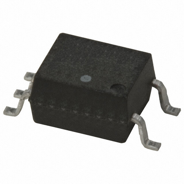
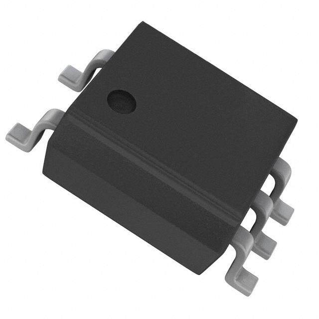
| 描述 | ISOLAT 3.75KVRMS 1CH OPEN 5SOP |
| 产品分类 | |
| 品牌 | CEL |
| 数据手册 | |
| 产品图片 |
|
| 产品型号 | PS9113-F3-AX |
| rohs | 无铅 / 符合限制有害物质指令(RoHS)规范要求 |
| 产品系列 | NEPOC |
| 上升/下降时间(典型值) | - |
| 传播延迟tpLH/tpHL(最大值) | 750ns, 500ns |
| 供应商器件封装 | 5-SO |
| 共模瞬态抗扰度(最小值) | 15kV/µs |
| 其它名称 | PS9113-F3-AX-ND |
| 包装 | 带卷 (TR) |
| 安装类型 | 表面贴装 |
| 封装/外壳 | 6-SOIC(0.173",4.40mm 宽,5 引线) |
| 工作温度 | -40°C ~ 100°C |
| 数据速率 | 1Mbps |
| 标准包装 | 2,500 |
| 电压-正向(Vf)(典型值) | 1.65V |
| 电压-电源 | 4.5 V ~ 30 V |
| 电压-隔离 | 3750Vrms |
| 电流-DC正向(If) | 25mA |
| 电流-输出/通道 | 15mA |
| 输入-输入侧1/输入侧2 | 1/0 |
| 输入类型 | DC |
| 输出类型 | 开路集电极 |
| 通道数 | 1 |


.jpg)

.jpg)


.jpg)

PDF Datasheet 数据手册内容提取
PS9113 Data Sheet R08DS0124EJ0200 1 Mbps, OPEN COLLECTOR OUTPUT Rev.2.00 HIGH CMR, INTELLIGENT POWER MODULE 5-PIN SOP Apr 13, 2015 (SO-5) PHOTOCOUPLER Description The PS9113 is an optically coupled isolator containing a GaAlAs LED on the input side and a photo diode and a signal processing circuit on the output side on one chip. The PS9113 is specified high CMR, high CTR and pulse width distortion with operating temperature. It is suitable for IPM drive. Features High instantaneous common mode rejection voltage (CM , CM = ±15 kV/µs MIN.) H L Small package (SO-5) High-speed response (t = 500 ns MAX., t = 750 ns MAX.) PIN CONNECTION PHL PLH (Top View) Maximum propagation delays (t – t = 270 ns TYP.) PLH PHL Pulse width distortion (|t – t | = 270 ns TYP.) 5 4 3 PHL PLH High isolation voltage (BV = 3 750 Vr.m.s.) 1. Anode Open collector output 2. Cathode Ordering number of taping product: PS9113-F3, F4: 2 500 pcs/reel 3. GND Pb-Free product 4. VO 5. VCC Safety standards UL approved: File No. E72422 1 2 DIN EN60747-5-5 (VDE0884-5):2011-11 approved: No. 40008902 (Option) APPLICATIONS IPM Driver General purpose inverter R08DS0124EJ0200 Rev.2.00 Page 1 of 13 Apr 13, 2015
PS9113 PACKAGE DIMENSIONS (UNIT: mm) 3.4+0.3 –0.1 5 4 3 7.0±0.3 4.4 1 2 0.2 +0.105–0.05 ± 1 2.6 0. 1 1.27 0.5±0.3 0. ± 1 0. 0.4+–00..0150 0.25 M FUNCTIONAL DIAGRAM 5 1 4 2 3 Shield LED Output ON L OFF H R08DS0124EJ0200 Rev.2.00 Page 2 of 13 Apr 13, 2015
PS9113 MARKING EXAMPLE Ni/Pd/AuPLATING 9113 Type Number N831 Assembly Lot No. 1 pin Mark *1 R Initial of Renesas (Engraved mark) N 8 31 Week Assembled Year Assembled (Last 1 Digit) Rank Code *1 Bar : Pb-Free R08DS0124EJ0200 Rev.2.00 Page 3 of 13 Apr 13, 2015
PS9113 ORDERING INFORMATION Part Number Order Number Solder Plating Packing Style Safety Standard Application Specification Approval Part Number*1 PS9113 PS9113-AX Pb-Free 20 pcs (Tape 20 pcs cut) Standard products PS9113 PS9113-F3 PS9113-F3-AX (Ni/Pd/Au) Embossed Tape 2500 pcs/reel (UL approved) PS9113-F4 PS9113-F4-AX PS9113-V PS9113-V-AX 20 pcs (Tape 20 pcs cut) DIN EN60747-5-5 PS9113-V-F3 PS9113-V-F3-AX Embossed Tape 2 500 pcs/reel (VDE0884-5):2011- 11 PS9113-V-F4 PS9113-V-F4-AX Approved (Option) Notes*: 1. For the application of the Safety Standard, following part number should be used. ABSOLUTE MAXIMUM RATINGS (T = 25°C, unless otherwise specified) A Parameter Symbol Ratings Unit Diode Forward Current*1 I 25 mA F Reverse Voltage V 5 V R Detector Supply Voltage V 0.5 to +25 V CC Output Voltage V 0.5 to +25 V O Output Current I 15 mA O Power Dissipation*2 P 100 mW C Isolation Voltage*3 BV 3750 Vr.m.s. Operating Ambient Temperature T 40 to +100 C A Storage Temperature T 55 to +125 C stg Notes*: 1. Reduced to 0.33 mA/°C at TA = 70°C or more. 2. Reduced to 1.9 mW/°C at TA = 70°C or more. 3. AC voltage for 1 minute at TA = 25°C, RH = 60% between input and output. Pins 1-2 shorted together, 3-5 shorted together. R08DS0124EJ0200 Rev.2.00 Page 4 of 13 Apr 13, 2015
PS9113 RECOMMENDED OPERATING CONDITIONS Parameter Symbol MIN. TYP. MAX. Unit High Level Input Current I 10 20 mA FH Output Voltage V 0 20 V O Supply Voltage V 4.5 15 20 V CC LED Off Voltage V 0 0.8 V F ELECTRICAL CHARACTERISTICS (T = –40 to +100°C, V = 15 V, unless otherwise A CC specified) Parameter Symbol Conditions MIN. TYP.*1 MAX. Unit Diode Forward Voltage V I = 10 mA 1.3 1.65 2.1 V F F Reverse Current I V = 3 V 200 A R R Terminal Capacitance C V = 0 V, f = 1 MHz, T = 25C 30 pF t A Detector Low Level Output Voltage V I = 10 mA, I = 2.4 mA 0.13 0.6 V OL F OL High Level Output Current I V = V = 20 V, V = 0.8 V 0.01 50 A OH CC O F High Level Supply Current I V = 20 V, V = 0.8 V, V = open 0.6 1.3 mA CCH CC F O Low Level Supply Current I V = 20 V, I = 10 mA, V = open 0.6 1.3 mA CCL CC F O Coupled Threshold Input Current V = 0.8 V, I = 0.75 mA I O O 1.5 5.0 mA (H L) FHL Current Transfer Ratio (I /I ) CTR I = 10 mA, V = 0.6 V 44 110 % C F F O Isolation Resistance V = 1 kV , RH = 40 to 60%, R I-O DC 1011 I-O T = 25C A Isolation Capacitance C V = 0 V, f = 1 MHz, TA = 25C 0.6 pF I-O Propagation Delay Time I = 10 mA, R = 20 k, C = 100 pF, t F L L 250 500 ns (H L)*2 PHL V = 1.5 V, V = 2.0 V THHL THLH Propagation Delay Time t 520 750 (L H)*2 PLH Maximum Propagation t t 200 270 650 Delays PLH PHL Pulse Width Distortion t -t 270 650 (PWD)*2 PHL PLH Common Mode T = 25C, I = 0 mA, V > 3.0 V, A F O Transient Immunity at High C V = 1.5 kV, RL = 20 k, 15 kV/s MH CM Level Output*3 C = 100 pF L Common Mode T = 25C, I = 10 mA, V < 1.0 V, A F O Transient Immunity at Low C V = 1.5 kV, R = 20 k, 15 kV/s ML CM L Level Output*3 C = 100 pF L R08DS0124EJ0200 Rev.2.00 Page 5 of 13 Apr 13, 2015
PS9113 Notes*: 1. Typical values at TA = 25°C. 2. Test circuit for propagation delay time Input IF(ON) Pulse input (IF = 10 mA) VCC = 15 V 50% IF (ON) 0.1 F RL = 20 k (PW = 10 s, Duty cycle = 1/10) VO (Monitor) 15 V CL = 100 pF Output Input VTHLH= 2.0 V (Monitor) 47 VTHHL = 1.5 V VOL tPHL tPLH CL includes probe and stray wiring capacitance. 3. Test circuit for common mode transient immunity 1.5 kV VCM 90% SW IF VCC = 15 V 10% 0.1 F RL = 20 k 0 V VO (Monitor) tr tf B A CL = 100 pF VO 15 V (Switch A: IF = 0 mA) 3.0 V 1.0 V VO VOL VCM (Switch B: IF = 10 mA) CL includes probe and stray wiring capacitance. USAGE CAUTIONS 1. This product is weak for static electricity by designed with high-speed integrated circuit so protect against static electricity when handling. 2. By-pass capacitor of 0.1 µF is used between V and GND near device. Also, ensure that the distance between the CC leads of the photocoupler and capacitor is no more than 10 mm. 3. Avoid storage at a high temperature and high humidity. R08DS0124EJ0200 Rev.2.00 Page 6 of 13 Apr 13, 2015
PS9113 TYPICAL CHARACTERISTICS (T = 25°C unless otherwise specified) A THRESHOLD INPUT CURRENT vs. SUPPLY CURRENT vs. AMBIENT TEMPERATURE AMBIENT TEMPERATURE 1200 5.000 µA)A) ICCL A) Vcc = 15V CH (CL (µ1000 ICCH L (m4.000 VIoo = = 0 0.7.85VmA CC H High Level Supply Current ILow Level Supply Current I 246800000000 VVIICCocCCc = HL= O : : 2 IpVF0eVF n= = 1 00m.8AV Threshold Input Current IF123...000000000 0 0.000 -50 -25 0 25 50 75 100 -50 -25 0 25 50 75 100 Ambient Temperature Ta (°C) Ambient Temperature Ta (°C) LOW LEVEL OUTPUT VOLTAGE vs. AMBIENT TEMPERATURE OUTPUT CURRENT vs. FORWARD CURRENT 0.600 16.00 V) Vcc = 15V 14.00 100°C L (0.500 IF = 10mA VO Io = 2.4mA A)12.00 e m 25°C ag0.400 o (10.00 put Volt0.300 urrent I 8.00 Ta = –40°C vel Out0.200 utput C 46..0000 e O w L0.100 2.00 o L Vo=0.6V 0.000 0.00 -50 -25 0 25 50 75 100 0.00 5.00 10.00 15.00 20.00 Ambient Temperature Ta (°C) Forward Current IF (mA) PROPAGATION DELAY TIME, OUTPUT CURRENT vs. MAXIMUM PROPAGATION DELAYS AMBIENT TEMPERATURE vs. FORWARD CURRENT s) n 1.100 ns)H ( 600 nt (Relative Value)01..900000 IVFo == 100.6mVA Time TPHL, TPLH (n Delays TPHL-TPL 345000000 TTPPLLHH-TPHL Curre0.800 Delayagatio 200 TPHL Output 0.700 gation m Prop 100 VCcLc = = 1 1050VpF a pu RL = 20KΩ om 0.600 Prxi 0 -50 -25 0 25 50 75 100 a 0 5 10 15 20 25 M Ambient Temperature Ta (°C) Forward Current IF (mA) R08DS0124EJ0200 Rev.2.00 Page 7 of 13 Apr 13, 2015
PS9113 PROPAGATION DELAYTIME, PROPAGATION DELAYTIME, MAXIMUM PROPAGATION DELAYS PULSE WIDTH DISTORTION vs.SUPPLY VOLTAGE vs.AMBIENTTEMPERATURE s) n ns)H (1800 ns) 600 TPLH (HL-TPL11460000 ICRFLL = == 1 12000m0KApΩF TPLH (D (ns) 500 TPLH L,P L,W HT1200 HP 400 TPays TPon PWD yTimeon Del1800000 yTimeDistorti 300 agation Delam Propagati 246000000 TPHL TPLH agation DelaPulse Width 120000 IVCFcL c= = =1 1 010m50VApF TPHL pu TPLH-TPHL p om o RL = 20KΩ Prxi 0 Pr 0 a 0 10 20 30 -40 -20 0 20 40 60 80 100 M SupplyVoltage Vcc (V) AmbientTemperatureTa (°C) PROPAGATION DELAYTIME, PROPAGATION DELAYTIME MAXIMUM PROPAGATION DELAYS vs.LOAD CAPACITANCE vs.LOAD RESISTANCE s) 1600 ns)H (n1000 e (ns)11240000 IVRFcL c= = =1 2 010m5KVAΩ TPLH L,TPLH (PHL-TPL 800 IVCFcL c= = =1 1 010m50VApF TPLH m HT yTi1000 TPays 600 gation Dela 680000 TPHL DelayTimeagation Del 400 TPLH-TPHL Propa 240000 gation m Prop 200 TPHL a pu om 0 Prxi 0 0 100 200 300 400 500 a 0 10 20 30 40 50 M Load Capacitance CL (pF) Load Resistance RL (KΩ) PROPAGATION DELAYTIME, MAXIMUM PROPAGATION DELAYS vs.LOAD RESISTANCE s) n ns)H ( 500 H (PL IF = 10mA TPLH LT Vcc = 5V TPHL- 400 CL = 15pF L,P HT TPLH-TPHL Ps Tay 300 meDel Tin Delayagatio 200 n p TPHL oo atiPr 100 gm a pu om Prxi 0 a 0 5 10 15 20 25 M Load Resistance RL (KΩ) R08DS0124EJ0200 Rev.2.00 Page 8 of 13 Apr 13, 2015
PS9113 TAPING SPECIFICATIONS (UNIT: mm) Outline and Dimensions (Tape) 1 0. 2.0±0.05 ± 4.0±0.1 1.5+–00.1 1.75 ±0.1 3.45 MAX. 4 7. 1 2 0. 0. ± ± 5 0 5. 2. 1 1.55±0.1 3.9±0.1 3.0±0.1 8.0±0.1 0.3±0.05 Tape Direction PS9113-F3 PS9113-F4 Outline and Dimensions (Reel) 2.0±0.5 2.0±0.5 13.0±0.2 0 0 2 2. 1. 0. ± ± ± 0 0 0 3 0 3. R 1.0 3 1 1 21.0±0.8 13.5±1.0 17.5±1.0 Packing: 2 500 pcs/reel R08DS0124EJ0200 Rev.2.00 Page 9 of 13 Apr 13, 2015
PS9113 RECOMMENDED MOUNT PAD DIMENSIONS (UNIT: mm) 1.45 8 0. 7 2 1. 5.5 R08DS0124EJ0200 Rev.2.00 Page 10 of 13 Apr 13, 2015
PS9113 NOTES ON HANDLING 1.Recommended soldering conditions (1)Infrared reflow soldering • Peak reflow temperature 260C or below (package surface temperature) • Time of peak reflow temperature 10 seconds or less • Time of temperature higher than 220C 60 seconds or less • Time to preheat temperature from 120 to 180C 12030 s • Number of reflows Three • Flux Rosin flux containing small amount of chlorine (The flux with a maximum chlorine content of 0.2 Wt% is recommended.) Recommended Temperature Profile of Infrared Reflow C) (heating) T (° to 10 s ure 260°C MAX. at 220°C er mp to 60 s e T e c 180°C a urf e S 120°C g 120±30 s a ck (preheating) a P Time (s) (2)Wave soldering Temperature 260C or below (molten solder temperature) Time 10 seconds or less Preheating conditions 120C or below (package surface temperature) Number of times One (Allowed to be dipped in solder including plastic mold portion.) Flux Rosin flux containing small amount of chlorine (The flux with a maximum chlorine content of 0.2 Wt% is recommended.) (3)Soldering by Soldering Iron Peak Temperature (lead part temperature) 350C or below Time (each pins) 3 seconds or less Flux Rosin flux containing small amount of chlorine (The flux with a maximum chlorine content of 0.2 Wt% is recommended.) (a)Soldering of leads should be made at the point 1.5 to 2.0 mm from the root of the lead (b)Please be sure that the temperature of the package would not be heated over 100C (4)Cautions Fluxes Avoid removing the residual flux with freon-based and chlorine-based cleaning solvent. R08DS0124EJ0200 Rev.2.00 Page 11 of 13 Apr 13, 2015
PS9113 2.Cautions regarding noise Be aware that when voltage is applied suddenly between the photocoupler’s input and output or between collector- emitters at startup, the output transistor may enter the on state, even if the voltage is within the absolute maximum ratings. USAGE CAUTIONS 1. Protect against static electricity when handling. 2. Avoid storage at a high temperature and high humidity. R08DS0124EJ0200 Rev.2.00 Page 12 of 13 Apr 13, 2015
PS9113 SPECIFICATION OF VDE MARKS LICENSE DOCUMENT Parameter Symbol Speck Unit Climatic test class (IEC 60068-1/DIN EN 60068-1) 40/100/21 Dielectric strength maximum operating isolation voltage Test voltage (partial discharge test, procedure a for type test and random UIORM 707 Vpeak test) Upr 1131 Vpeak Upr = 1.6 UIORM, Pd 5 pC Test voltage (partial discharge test, procedure b for all devices) Upr 1 326 Vpeak Upr = 1.875 UIORM, Pd 5 pC Highest permissible overvoltage UTR 6 000 Vpeak Degree of pollution (DIN EN 60664-1 VDE 0110 Part 1) 2 Comparative tracking index ((IEC 60112/DIN EN 60112 (VDE 0303 Part CTI 175 11)) Material group (DIN EN 60664-1 VDE 0110 Part 1) III a Storage temperature range Tstg –55 to +125 °C Operating temperature range TA –40 to +100 °C Isolation resistance, minimum value VIO = 500 V dc at TA = 25°C Ris MIN. 1012 Ω VIO = 500 V dc at TA MAX. at least 100°C Ris MIN. 1011 Ω Safety maximum ratings (maximum permissible in case of fault, see thermal derating curve) Package temperature Tsi 150 °C Current (input current IF, Psi = 0) Isi 200 mA Power (output or total power dissipation) Psi 300 mW Isolation resistance VIO = 500 V dc at TA = Tsi Ris MIN. 109 Ω R08DS0124EJ0200 Rev.2.00 Page 13 of 13 Apr 13, 2015
This product uses gallium arsenide (GaAs). Caution GaAs Products GaAs vapor and powder are hazardous to human health if inhaled or ingested, so please observe the following points. •Follow related laws and ordinances when disposing of the product. If there are no applicable laws and/or ordinances, dispose of the product as recommended below. 1.Commission a disposal company able to (with a license to) collect, transport and dispose of materials that contain arsenic and other such industrial waste materials. 2.Exclude the product from general industrial waste and household garbage, and ensure that the product is controlled (as industrial waste subject to special control) up until final disposal. •Do not burn, destroy, cut, crush, or chemically dissolve the product. •Do not lick the product or i any way allow it to enter the mouth. All trademarks and registered trademarks are the property of their respective owners.
NOTICE 1. Descriptions of circuits, software and other related information in this document are provided only to illustrate the operation of semiconductor products and application examples. You are fully responsible for the incorporation of these circuits, software, and information in the design of your equipment. California Eastern Laboratories and Renesas Electronics assumes no responsibility for any losses incurred by you or third parties arising from the use of these circuits, software, or information. 2. California Eastern Laboratories has used reasonable care in preparing the information included in this document, but California Eastern Laboratories does not warrant that such information is error free. California Eastern Laboratories and Renesas Electronics assumes no liability whatsoever for any damages incurred by you resulting from errors in or omissions from the information included herein. 3. California Eastern Laboratories and Renesas Electronics do not assume any liability for infringement of patents, copyrights, or other intellectual property rights of third parties by or arising from the use of Renesas Electronics products or technical information described in this document. No license, express, implied or otherwise, is granted hereby under any patents, copyrights or other intellectual property rights of California Eastern Laboratories or Renesas Electronics or others. 4. You should not alter, modify, copy, or otherwise misappropriate any Renesas Electronics product, whether in whole or in part. California Eastern Laboratories and Renesas Electronics assume no responsibility for any losses incurred by you or third parties arising from such alteration, modification, copy or otherwise misappropriation of Renesas Electronics product. 5. Renesas Electronics products are classified according to the following two quality grades: “Standard” and “High Quality”. The recommended applications for each Renesas Electronics product depends on the product’s quality grade, as indicated below. “Standard”: Computers; office equipment; communications equipment; test and measurement equipment; audio and visual equipment; home electronic appliances; machine tools; personal electronic equipment; and industrial robots etc. “High Quality”: Transportation equipment (automobiles, trains, ships, etc.); traffic control systems; anti-disaster systems; anti-crime systems; and safety equipment etc. Renesas Electronics products are neither intended nor authorized for use in products or systems that may pose a direct threat to human life or bodily injury (artificial life support devices or systems, surgical implantations etc.), or may cause serious property damages (nuclear reactor control systems, military equipment etc.). You must check the quality grade of each Renesas Electronics product before using it in a particular application. You may not use any Renesas Electronics product for any application for which it is not intended. California Eastern Laboratories and Renesas Electronics shall not be in any way liable for any damages or losses incurred by you or third parties arising from the use of any Renesas Electronics product for which the product is not intended by California Eastern Laboratories or Renesas Electronics. 6. You should use the Renesas Electronics products described in this document within the range specified by California Eastern Laboratories, especially with respect to the maximum rating, operating supply voltage range, movement power voltage range, heat radiation characteristics, installation and other product characteristics. California Eastern Laboratories shall have no liability for malfunctions or damages arising out of the use of Renesas Electronics products beyond such specified ranges. 7. Although Renesas Electronics endeavors to improve the quality and reliability of its products, semiconductor products have specific characteristics such as the occurrence of failure at a certain rate and malfunctions under certain use conditions. Further, Renesas Electronics products are not subject to radiation resistance design. Please be sure to implement safety measures to guard them against the possibility of physical injury, and injury or damage caused by fire in the event of the failure of a Renesas Electronics product, such as safety design for hardware and software including but not limited to redundancy, fire control and malfunction prevention, appropriate treatment for aging degradation or any other appropriate measures. Because the evaluation of microcomputer software alone is very difficult, please evaluate the safety of the final products or systems manufactured by you. 8. Please contact a California Eastern Laboratories sales office for details as to environmental matters such as the environmental compatibility of each Renesas Electronics product. Please use Renesas Electronics products in compliance with all applicable laws and regulations that regulate the inclusion or use of controlled substances, including without limitation, the EU RoHS Directive. California Eastern Laboratories and Renesas Electronics assume no liability for damages or losses occurring as a result of your noncompliance with applicable laws and regulations. 9. Renesas Electronics products and technology may not be used for or incorporated into any products or systems whose manufacture, use, or sale is prohibited under any applicable domestic or foreign laws or regulations. You should not use Renesas Electronics products or technology described in this document for any purpose relating to military applications or use by the military, including but not limited to the development of weapons of mass destruction. When exporting the Renesas Electronics products or technology described in this document, you should comply with the applicable export control laws and regulations and follow the procedures required by such laws and regulations. 10. It is the responsibility of the buyer or distributor of California Eastern Laboratories, who distributes, disposes of, or otherwise places the Renesas Electronics product with a third party, to notify such third party in advance of the contents and conditions set forth in this document, California Eastern Laboratories and Renesas Electronics assume no responsibility for any losses incurred by you or third parties as a result of unauthorized use of Renesas Electronics products. 11. This document may not be reproduced or duplicated in any form, in whole or in part, without prior written consent of California Eastern Laboratories. 12. Please contact a California Eastern Laboratories sales office if you have any questions regarding the information contained in this document or Renesas Electronics products, or if you have any other inquiries. NOTE 1: “Renesas Electronics” as used in this document means Renesas Electronics Corporation and also includes its majority-owned subsidiaries. NOTE 2: “Renesas Electronics product(s)” means any product developed or manufactured by or for Renesas Electronics. NOTE 3: Products and product information are subject to change without notice. CEL Headquarters • 4590 Patrick Henry Drive, Santa Clara, CA 95054 • Phone (408) 919-2500 • www.cel.com For a complete list of sales offices, representatives and distributors, Please visit our website: www.cel.com/contactus