 Datasheet下载
- 型号: PS7241-1A-F3-A
- 制造商: CEL
- 库位|库存: xxxx|xxxx
- 要求:
| 数量阶梯 | 香港交货 | 国内含税 |
| +xxxx | $xxxx | ¥xxxx |
查看当月历史价格
查看今年历史价格
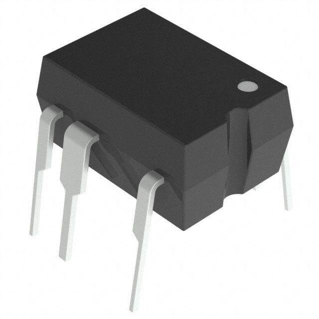
PS7241-1A-F3-A产品简介:
ICGOO电子元器件商城为您提供PS7241-1A-F3-A由CEL设计生产,在icgoo商城现货销售,并且可以通过原厂、代理商等渠道进行代购。 PS7241-1A-F3-A价格参考。CELPS7241-1A-F3-A封装/规格:固态继电器, 固体继电器 继电器 SPST-NO(1 Form A) 4-SOP(0.173",4.40mm)。您可以下载PS7241-1A-F3-A参考资料、Datasheet数据手册功能说明书,资料中有PS7241-1A-F3-A 详细功能的应用电路图电压和使用方法及教程。
CEL品牌的PS7241-1A-F3-A固态继电器(SSR)是一款高性能的电气控制元件,广泛应用于各种工业自动化、家电及照明控制系统中。该型号的主要应用场景包括但不限于以下几种:

 1. 工业自动化控制
   PS7241-1A-F3-A适用于工业自动化设备中的负载切换和控制。例如,在生产线上的电机启动与停止、传送带的速度控制、加热器的温度调节等场景中,该继电器能够实现无触点开关操作,减少机械磨损,延长设备寿命。其高可靠性和长寿命特性使其在恶劣的工业环境中表现尤为出色。

 2. 家用电器
   在家用电器领域,如空调、冰箱、洗衣机等设备中,PS7241-1A-F3-A可用于控制压缩机、风扇、加热元件等部件的工作状态。它能够快速响应控制信号,确保电器设备的稳定运行,并且由于其低噪音、无火花的特点,提升了用户的使用体验。

 3. 照明控制系统
   在智能照明系统中,PS7241-1A-F3-A可以用于控制LED灯、荧光灯等光源的开关和调光功能。它能够与楼宇自动化系统集成,实现远程控制和定时开关,从而提高能源利用效率,降低能耗。

 4. 电力控制系统
   该型号的固态继电器还可用于电力系统的保护和控制,例如在配电柜中作为过载保护装置,或在不间断电源(UPS)系统中进行电源切换。其快速响应时间和低导通电阻特性,使得它能够在毫秒级时间内完成电流的通断操作,确保电力系统的安全性和稳定性。

 5. 医疗设备
   在医疗设备中,如X光机、CT扫描仪等精密仪器中,PS7241-1A-F3-A用于控制高压发生器、冷却风扇等关键部件。其高精度和高可靠性保证了医疗设备的安全运行,减少了故障发生的可能性。

总之,CEL品牌的PS7241-1A-F3-A固态继电器凭借其优异的性能和广泛的适用性,成为众多行业不可或缺的关键组件。
| 参数 | 数值 |
| 产品目录 | |
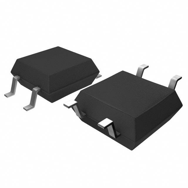
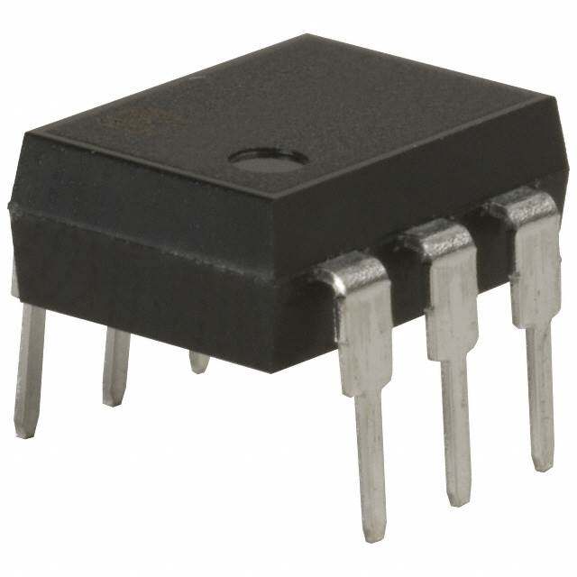
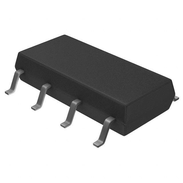
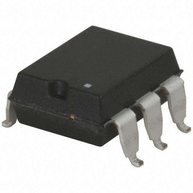
| 描述 | SSR OCMOS FET 120MA NO 4-SOP TR |
| 产品分类 | |
| 品牌 | CEL |
| 数据手册 | |
| 产品图片 |
|
| 产品型号 | PS7241-1A-F3-A |
| rohs | 无铅 / 符合限制有害物质指令(RoHS)规范要求 |
| 产品系列 | PS, OCMOS |
| 产品培训模块 | http://www.digikey.cn/PTM/IndividualPTM.page?site=cn&lang=zhs&ptm=14010 |
| 产品目录绘图 |
|
| 产品目录页面 | |
| 供应商器件封装 | 4-SOP(2.54mm) |
| 其它名称 | PS7241-1A-F3-ADKR |
| 包装 | Digi-Reel® |
| 安装类型 | 表面贴装 |
| 导通电阻 | 30 欧姆 |
| 封装/外壳 | 4-SOP(0.173",4.40mm) |
| 标准包装 | 1 |
| 电压-负载 | 0 ~ 400 V |
| 电压-输入 | 1.2VDC |
| 电路 | SPST-NO(1 Form A) |
| 端子类型 | 鸥翼型 |
| 继电器类型 | |
| 负载电流 | 120mA |
| 输出类型 | AC,DC |


- 商务部:美国ITC正式对集成电路等产品启动337调查
- 曝三星4nm工艺存在良率问题 高通将骁龙8 Gen1或转产台积电
- 太阳诱电将投资9.5亿元在常州建新厂生产MLCC 预计2023年完工
- 英特尔发布欧洲新工厂建设计划 深化IDM 2.0 战略
- 台积电先进制程称霸业界 有大客户加持明年业绩稳了
- 达到5530亿美元!SIA预计今年全球半导体销售额将创下新高
- 英特尔拟将自动驾驶子公司Mobileye上市 估值或超500亿美元
- 三星加码芯片和SET,合并消费电子和移动部门,撤换高东真等 CEO
- 三星电子宣布重大人事变动 还合并消费电子和移动部门
- 海关总署:前11个月进口集成电路产品价值2.52万亿元 增长14.8%

PDF Datasheet 数据手册内容提取
Solid State Relay OCMOS FET PS7241-1A D 4-PIN SOP 400 V BREAK DOWN VOLTAGE 1-ch Optical Coupled MOS FET E DESCRIPTION U The PS7241-1A is a solid state relay containing GaAs LEDs on the light emitting side (input side) and normally open (N.O.) contact MOS FETs on the output side. It is suitable for analog signal control because of its low offset and high linearity. N FEATURES • Small and thin package (4-pin SOP, Height = 2.1 mm) • 1 channel type (1 a output) • Low LED operating current (IF = 2 mA) I • Designed for AC/DC switching line changer T • Low offset voltage • Ordering number of taping product: PS7241-1A-E3, E4, E5, F3, F4 • UL approved: File No. E72422 (S) N • BSI approved: No. 8241/8242 • CSA approved: No. CA 101391 • VDE approved: No. 121302 ÜG O APPLICATIONS • Laptop PC, PDA • Modem card • Telephone, FAX C • Measurement equipment S I D Document No. PN10301EJ01V1DS (1st edition) The mark (cid:144) shows major revised points. (Previous No. P13438EJ5V0DS00) Date Published February 2003 CP(K)
PS7241-1A PACKAGE DIMENSIONS in millimeters D 4.0±0.5 TOP VIEW 4 3 E 1. LED Anode 2. LED Cathode 3. MOS FET 4. MOS FET U 1 2 7.0±0.3 N 4.4 +0.0805–0.05 +0.100.15–0.05 I 2. T +0.085–0.05 2.54 0.5±0.3 0.0 0.40+–00..1005 0.25 M N O C S I D 2 Data Sheet PN10301EJ01V1DS
PS7241-1A ORDERING INFORMATION (Solder Contains Lead) *1 Part Number Package Packing Style Application Part Number D PS7241-1A 4-pin SOP Magazine case 100 pcs PS7241-1A PS7241-1A-E3 Embossed Tape 900 pcs/reel PS7241-1A-E4 E PS7241-1A-E5 Embossed Tape 1 000 pcs/reel PS7241-1A-F3 Embossed Tape 3 500 pcs/reel PS7241-1A-F4 U *1 For the application of the Safety Standard, following part number should be used. ORDERING INFORMATION (Pb-Free) N *1 Part Number Package Packing Style Application Part Number PS7241-1A-A 4-pin SOP Magazine case 100 pcs PS7241-1A I PS7241-1A-E3-A Embossed Tape 900 pcs/reel PS7241-1A-E4-A T PS7241-1A-E5-A Embossed Tape 1 000 pcs/reel PS7241-1A-F3-A Embossed Tape 3 500 pcs/reel N PS7241-1A-F4-A *1 For the application of the Safety Standard, following part number should be used. O ABSOLUTE MAXIMUM RATINGS (TA = 25 °C, unless otherwise specified) Parameter Symbol Ratings Unit Diode Forward Current (DCC) IF 50 mA Reverse Voltage VR 5.0 V Power Dissipation PD 50 mW Peak FoSrward Current *1 IFP 1 A MOS FET Break Down Voltage VL 400 V Continuous Load Current IL 120 mA IPulse Load Current*2 ILP 240 mA (AC/DC Connection) D Power Dissipation PD 300 mW Isolation Voltage *3 BV 1 500 Vr.m.s. Total Power Dissipation PT 350 mW Operating Ambient Temperature TA −40 to +85 °C Storage Temperature Tstg −40 to +100 °C *1 PW = 100 µs, Duty Cycle = 1 % *2 PW = 100 ms, 1 shot *3 AC voltage for 1 minute at TA = 25 °C, RH = 60 % between input and output Data Sheet PN10301EJ01V1DS 3
PS7241-1A RECOMMENDED OPERATING CONDITIONS (TA = 25 °C) D Parameter Symbol MIN. TYP. MAX. Unit LED Operating Current IF 2 10 20 mA LED Off Voltage VF 0 0.5 V E ELECTRICAL CHARACTERISTICS (TA = 25 °C) Parameter Symbol Conditions MIN. TYP. MAX. Unit U Diode Forward Voltage VF I F = 10 mA 1.2 1.4 V Reverse Current IR V R = 5 V 5.0 µA MOS FET Off-state Leakage ILoff V D = 400 V N 0.03 1.0 µA Current Output Capacitance Cout V D = 0 V, f = 1 MHz 54 pF Coupled LED On-state Current IFon I L = 120 mA 2.0 mA I On-state Resistance Ron1 I F = 10 mA, IL = 10 mA 18 30 Ω T Ron2 I F = 10 mA, IL = 120 mA, t ≤ 10 ms 15 25 Turn-on Time*1 ton I F = 10 mA, VO = 5 V, RL = 500 Ω, 0.5 2.0 ms Turn-off Time*1 toff PW ≥ 10 ms 0.07 0.2 N Isolation Resistance RI-O V I-O = 1.0 kVDC 109 Ω Isolation Capacitance CI-O V = 0 V, f = 1 MHz 0.5 pF O *1 Test Circuit for Switching Time IF Pulse Input VL Input 50 % C 0 S VO = 5 V 90 % Input monitor VOmonitor Output Rin RL 10 % I ton toff D 4 Data Sheet PN10301EJ01V1DS
PS7241-1A TYPICAL CHARACTERISTICS (TA = 25 °C, unless otherwise specified) MAXIMUM FORWARD CURRENT vs. MAXIMUM LOAD CURRENT vs. AMBIENT TEMPERATURE AMBIENT TEMPERATURE D 100 300 A) m A) ent I (F 80 nt I (mL 200 E Curr 60 urre d C ar d w a or 40 Lo U F m 100 m u u m m 20 xi axi Ma M 0 0 N –25 0 25 50 7585 100 –25 0 25 50 7585 100 Ambient Temperature TA (˚C) Ambient Temperature TA (˚C) FORWARD VOLTAGE vs. OUTPUT CAPACITANCE vs. I AMBIENT TEMPERATURE APPLIED VOLTAGE 1.8 T200 f = 1 MHz V (V)F 1.6 IF = 53210000 mmmmAAAA N C (pF)out 150 Voltage 1.4 51 mmAA acitance 100 d 1.2 p ar O Ca Forw 1.0 utput 50 O 0.8 –25 0 25 C50 75 100 0 20 40 60 80 100 120 Ambient Temperature TA (˚C) Applied Voltage VD (V) OFF-STATE LEAKAGE CURRENT vs. APPLIEDS VOLTAGE LOAD CURRENT vs. LOAD VOLTAGE 10–5 200 IF = 10 mA A) nt I (Loff 10–6I TA = 85 ˚C mA) 100 e Curre 1D0–7 ent I (L akag 25 ˚C Curr –4.0 –2.0 0 2.0 4.0 ate Le 10–8 Load –100 st Off- 10–9 –200 0 100 200 300 400 500 Applied Voltage VD (V) Load Voltage VL (V) Data Sheet PN10301EJ01V1DS 5
PS7241-1A NORMALIZED ON-STATE RESISTANCE vs. AMBIENT TEMPERATURE ON-STATE RESISTANCE DISTRIBUTION 3.0 30 nce Ron 2.5 INaFt o =Tr mA1 0=a l mi2z5eA d˚, C to, 1.0 25 InIFL === 511000D pmmcAAs,, Resista 2.0 IL = 10 mA pcs) 20 ate 1.5 er ( 15 E d On-st 1.0 Numb 10 e maliz 0.5 5 U or N 0.0 0 –25 0 25 50 75 100 16 18 20 22 24 Ambient Temperature TA (˚C) NOn-state Resistance Ron (Ω) TURN-ON TIME vs. FORWARD CURRENT TURN-OFF TIME vs. FORWARD CURRENT 3.0 I0.30 VO = 5 V VO = 5 V 2.5 T0.25 s) s) m m e t (on 2.0 N e t (off 0.20 m 1.5 m0.15 Ti Ti on off n- 1.0 n-0.10 ur ur T T 0.5 O 0.05 0 5 10 15 20 25 30 0 5 10 15 20 25 30 Forward Current IF (mA) Forward Current IF (mA) C TURN-ON TIME DISTRIBUTION TURN-OFF TIME DISTRIBUTION 30 30 n = 50 pcs, n = 50 pcs, S IF = 10 mA, IF = 10 mA, 25 VO = 5 V 25 VO = 5 V s) 20 s) 20 c c p I p er ( 15 er ( 15 b D b m m u u N 10 N 10 5 5 0 0 0.4 0.5 0.6 0.7 0.8 0.04 0.06 0.08 0.10 0.12 Turn-on Time ton (ms) Turn-off Time toff (ms) 6 Data Sheet PN10301EJ01V1DS
PS7241-1A NORMALIZED TURN-ON TIME vs. NORMALIZED TURN-OFF TIME vs. AMBIENT TEMPERATURE AMBIENT TEMPERATURE 3.0 3.0 Normalized to 1.0 NormalizedD to 1.0 me ton 2.5 IVaFt O =T = A1 50= Vm25A ˚, C, me toff 2.5 aIVFt O =T = A1 50= Vm25A ˚, C, Ti 2.0 Ti 2.0 Turn-on 1.5 Turn-off 1.5 E malized 1.0 malized 1.0 Nor 0.5 Nor 0.5 U 0.0 0.0 –25 0 25 50 75 100 –25 0 25 50 75 100 Ambient Temperature TA (˚C) NAmbient Temperature TA (˚C) Remark The graphs indicate nominal characteristics. I T N O C S I D Data Sheet PN10301EJ01V1DS 7
PS7241-1A TAPING SPECIFICATIONS (in millimeters) D Outline and Dimensions (Tape) 1 0. 2.0±0.05 ± 5 E 4.0±0.1 1.5+–00. 1 1.7 2.9 MAX. 5 2 5.5±0.0 12.0±0. 7.4±0.1 U 1.55±0.1 4.6±0.1 2.4±0.1 8.0±0.1 0.3 N Tape Direction I T PS7241-1A-E3 PS7241-1A-E4 N O Outline and Dimensions (Reel) 2.0±0.5 C 2.0±0.5 S φ13.0±0.2 φ+0 180–1.5 +160–0 I R 1.0 φ φ21.0±0.8 13.5±1.0 D 17.5±1.0 11.9 to 15.4 Outer edge of Packing: 900 pcs/reel flange 8 Data Sheet PN10301EJ01V1DS
PS7241-1A Outline and Dimensions (Tape) D 1 0. 2.0±0.1 ± 5 4.0±0.1 7 2.4±0.3 1.55±0.05 1. E 1 3 0. 0. 1 5± 0± ±0. 5. 12. 4.4 1.6±0.1 7.4±0.1 0.3±0U.05 12.0±0.3 N Tape Direction I PS7241-1A-E5 T N O Outline and Dimensions (Reel) 2.0 C 60 S 2.0±0.5 255±2.0 80±1.0 13.0±0.5 4 I 2.5 D 13.5±1.0 Packing: 1 000 pcs/reel Data Sheet PN10301EJ01V1DS 9
PS7241-1A Outline and Dimensions (Tape) D 1 0. 2.0±0.05 ± 5 4.0±0.1 1.5+–00. 1 1.7 2.9 MAX. E 5 2 5.5±0.0 12.0±0. 7.4±0.1 1.55±0.1 4.6±0.1 2.4±0.1 U 8.0±0.1 0.3 N Tape Direction I PS7241-1A-F3 PS7241-1A-F4 T N O Outline and Dimensions (Reel) 2.0±0.5 C 2.0±0.5 φ13.0±0.2 0 S 0±2. 1.0 0.2 3 ± ± 3 0 0 R 1.0 φ21.0±0.8 φ φ10 φ13. 13.5±1.0 I 17.5±1.0 D 11.9 to 15.4 Outer edge of Packing: 3 500 pcs/reel flange 10 Data Sheet PN10301EJ01V1DS
PS7241-1A RECOMMENDED SOLDERING CONDITIONS (1) Infrared reflow soldering • Peak reflow temperature 260°C or below (package surface temperature) D • Time of peak reflow temperature 10 seconds or less • Time of temperature higher than 220°C 60 seconds or less • Time to preheat temperature from 120 to 180°C 120±30 s • Number of reflows Three E • Flux Rosin flux containing small amount of chlorine (The flux with a maximum chlorine content of 0.2 Wt% is recommended.) Recommended Temperature Profile of Infrared RUeflow C) N T (˚ (htoe a1t0in sg) e ur 260˚C MAX. erat 220˚C p I m to 60 s e T e T c 180˚C a urf S 120˚C ge 120±30 s ka (preheating)N c a P O Time (s) (2) Wave soldering C • Temperature 260°C or below (molten solder temperature) • Time 10 seconds or less • Preheating conditions 120°C or below (package surface temperature) • Number of timeSs One • Flux Rosin flux containing small amount of chlorine (The flux with a maximum chlorine content of 0.2 Wt% is recommended.) I (3) Cautions • FDluxes Avoid removing the residual flux with freon-based and chlorine-based cleaning solvent. Data Sheet PN10301EJ01V1DS 11
4590 Patrick Henry Drive Santa Clara, CA 95054-1817 Telephone: (408) 919-2500 Facsimile: (408) 988-0279 D E Subject: Compliance with EU Directives U CEL certifies, to its knowledge, that semiconductor and laser products detailed below are compliant with the requirements of European Union (EU) Directive 2002/95/EC Restriction on Use of Hazardous Substances in electrical and electronic equipment (RoHS) and the requirements of EU Directive 2003/11/EC Restriction on Penta and Octa BDE. N CEL Pb-free products have the same base part number with a suffix added. The suffix –A indicates that the device is Pb-free. The –AZ suffix is used to designate devices containing Pb which are exempted from the requirement of RoHS directive (*). In all cases the devices have Pb-free terminals. All devices with these suffixes meet the requirements of tIhe RoHS directive. T This status is based on CEL’s understanding of the EU Directives and knowledge of the materials that go into its products as of the date of disclosure of this information. Restricted Substance Concentration LNimit per RoHS Concentration contained per RoHS (values are not yet fixed) in CEL devices -A -AZ Lead (Pb) < 1000 PPM Not Detected (*) O Mercury < 1000 PPM Not Detected Cadmium < 100 PPM Not Detected Hexavalent Chromium < 1000 PPM Not Detected C PBB < 1000 PPM Not Detected PBDE < 1000 PPM Not Detected S If you should have any additional questions regarding our devices and compliance to environmental standards, please do not hesitate to contact your local representative. Important InfIormation and Disclaimer: Information provided by CEL on its website or in other communications concerting the substance content of its products represents knowledge and belief as of the date that it is provided. CEL bases its knowledge and belief on information provideDd by third parties and makes no representation or warranty as to the accuracy of such information. Efforts are underway to better integrate information from third parties. CEL has taken and continues to take reasonable steps to provide representative and accurate information but may not have conducted destructive testing or chemical analysis on incoming materials and chemicals. CEL and CEL suppliers consider certain information to be proprietary, and thus CAS numbers and other limited information may not be available for release. In no event shall CEL’s liability arising out of such information exceed the total purchase price of the CEL part(s) at issue sold by CEL to customer on an annual basis. See CEL Terms and Conditions for additional clarification of warranties and liability.