ICGOO在线商城 > 隔离器 > 光隔离器 - 晶体管,光电输出 > PS2805C-1-F3-A
 Datasheet下载
- 型号: PS2805C-1-F3-A
- 制造商: CEL
- 库位|库存: xxxx|xxxx
- 要求:
| 数量阶梯 | 香港交货 | 国内含税 |
| +xxxx | $xxxx | ¥xxxx |
查看当月历史价格
查看今年历史价格
PS2805C-1-F3-A产品简介:
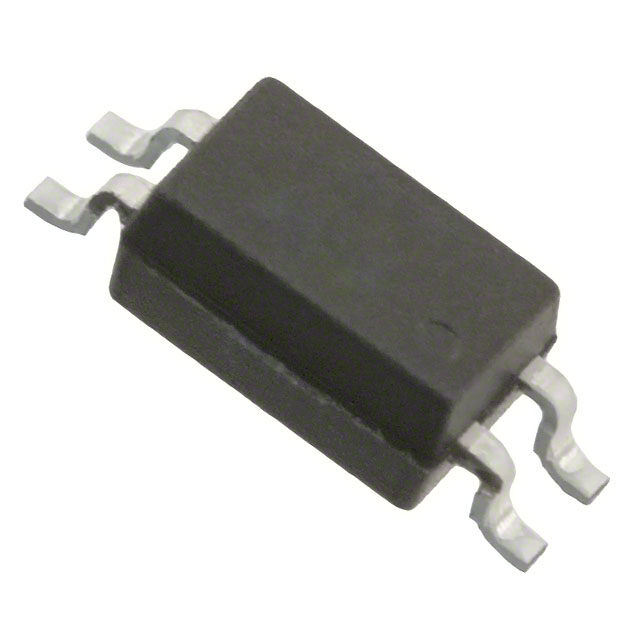
ICGOO电子元器件商城为您提供PS2805C-1-F3-A由CEL设计生产,在icgoo商城现货销售,并且可以通过原厂、代理商等渠道进行代购。 PS2805C-1-F3-A价格参考¥2.45-¥2.45。CELPS2805C-1-F3-A封装/规格:光隔离器 - 晶体管,光电输出, Optoisolator Transistor Output 2500Vrms 1 Channel 4-SSOP。您可以下载PS2805C-1-F3-A参考资料、Datasheet数据手册功能说明书,资料中有PS2805C-1-F3-A 详细功能的应用电路图电压和使用方法及教程。
CEL的PS2805C-1-F3-A是一款光隔离器(光电晶体管输出型),广泛应用于需要电气隔离的电路中。其主要功能是通过光信号实现输入与输出之间的电气隔离,有效防止噪声干扰、电压冲击和接地环路问题。

典型应用场景包括:工业自动化控制系统中的信号隔离,如PLC输入/输出模块;开关电源中的反馈回路,用于稳定输出电压并隔离高低压部分;通信设备中实现级间隔离,提升系统抗干扰能力;家用电器(如空调、洗衣机)的微控制器与高电压驱动电路之间的隔离控制;以及医疗电子设备中对安全隔离要求较高的场合。

PS2805C-1-F3-A具有高隔离电压、良好的温度稳定性及紧凑的封装,适用于空间受限且对可靠性要求高的设计。其晶体管输出结构便于直接驱动后续逻辑电路或继电器,适合直流信号传输与控制。整体而言,该器件在保障系统安全、提升抗噪性能方面发挥重要作用。
| 参数 | 数值 |
| 产品目录 | |
| 描述 | OPTOISOLATOR 2.5KV TRANS 4SOIC晶体管输出光电耦合器 16pin SSOP Quad SGL TR AC Cplr |
| 产品分类 | |
| 品牌 | CEL |
| 产品手册 | |
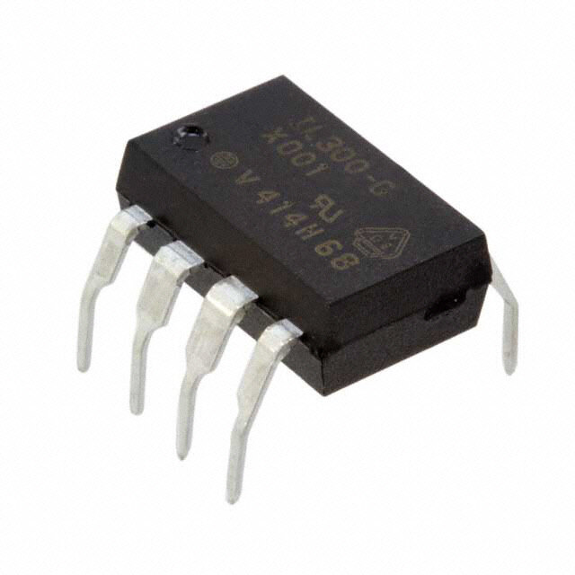
| 产品图片 |
|
| rohs | 符合RoHS无铅 / 符合限制有害物质指令(RoHS)规范要求 |
| 产品系列 | 光耦合器/光电耦合器,晶体管输出光电耦合器,CEL PS2805C-1-F3-ANEPOC |
| 数据手册 | |
| 产品型号 | PS2805C-1-F3-A |
| Vce饱和值(最大值) | 300mV |
| 上升/下降时间(典型值) | 5µs, 7µs |
| 产品目录页面 | |
| 产品种类 | 晶体管输出光电耦合器 |
| 供应商器件封装 | 4-SSOP |
| 其它名称 | PS2805C-1-F3-ATR |
| 其它图纸 |
|
| 包装 | 带卷 (TR) |
| 商标 | CEL |
| 安装类型 | 表面贴装 |
| 封装 | Reel |
| 封装/外壳 | 4-SOIC (0.173", 4.40mm) |
| 封装/箱体 | SSOP-4 |
| 工作温度 | -55°C ~ 100°C |
| 工厂包装数量 | 3500 |
| 打开/关闭时间(典型值) | 10µs, 7µs |
| 最大工作温度 | + 100 C |
| 最大正向二极管电压 | 1.4 V |
| 最大输入二极管电流 | 5 mA |
| 最大集电极/发射极电压 | 80 V |
| 最大集电极/发射极饱和电压 | 0.3 V |
| 最小工作温度 | - 55 C |
| 标准包装 | 3,500 |
| 正向电流 | 5 mA |
| 每芯片的通道数量 | 1 Channel |
| 电压-正向(Vf)(典型值) | 1.2V |
| 电压-输出(最大值) | 80V |
| 电压-隔离 | 2500Vrms |
| 电流-DC正向(If) | 30mA |
| 电流-输出/通道 | 30mA |
| 电流传输比(最大值) | 400% @ 5mA |
| 电流传输比(最小值) | 50% @ 5mA |
| 电流传递比 | 50 % to 400 % |
| 绝缘电压 | 2500 Vrms |
| 输入类型 | AC,DC |
| 输出类型 | 晶体管 |
| 输出设备 | NPN Phototransistor |
| 通道数 | 1 |


.jpg)

.jpg)


(B)(TU)-VG.jpg)

PDF Datasheet 数据手册内容提取
A Business Partner of Renesas Electronics Corporation. PS2805C-1, PS2805C-4 Data Sheet R08DS0074EJ0300 HIGH ISOLATION VOLTAGE AC INPUT RESPONSE TYPE Rev.3.00 SSOP PHOTOCOUPLER Jan 9, 2013 DESCRIPTION The PS2805C-1 and PS2805C-4 are optically coupled isolators containing a GaAs light emitting diode and an NPN silicon phototransistor in a plastic SSOP for high density applications to realize an excellent cost performance. This package has shield effect to cut off ambient light. FEATURES PIN CONNECTION • High isolation voltage (BV = 2 500 Vr.m.s.) (Top View) • Small and thin package (4, 16-pin SSOP, Pin pitch 1.27 mm) • High collector to emitter voltage (V : 80 V) PS2805C-1 CEO • AC input response 4 3 <R> • Ordering number of tape product: PS2805C-1-F3, PS2805C-4-F3 1.Anode, Cathode • Pb-Free product 2.Cathode, Anode 3.Emitter <R> • Safety standards 4.Collector • UL approved: No. E72422 1 2 • CSA approved: No. CA 101391 (CA5A, CAN/CSA-C22.2 60065, 60950) • BSI approved (BS EN 60065, BS EN 60950) (PS2805C-1 only) PS2805C-4 • DIN EN 60747-5-5 (VDE 0884-5) approved (Option) 16151413121110 9 APPLICATIONS • Programmable logic controllers 1 2 3 4 5 6 7 8 • OA equipment • Measuring instruments 1. 3. 5. 7. Anode, Cathode • Hybrid IC 2. 4. 6. 8. Cathode, Anode 9.11. 13. 15. Emitter 10.12. 14. 16. Collector The mark <R> shows major revised points. The revised points can be easily searched by copying an "<R>" in the PDF file and specifying it in the "Find what:" field. R08DS0074EJ0300 Rev.3.00 Page 1 of 12 Jan 9, 2013
A Business Partner of Renesas Electronics Corporation. PS2805C-1, PS2805C-4e PACKAGE DIMENSIONS (UNIT: mm) PS2805C-1 PS2805C-4 2.7±0.3 10.3±0.3 4 3 16 9 1 2 1 8 7.0±0.3 7.0±0.3 2.0±0.1 0.1±0.1 +0.100.15–0.05 4.4 +0.32.0–0.2 +0.100.15–0.05 4.4 0.5±0.3 0.1 0.40+–00..1005 0.12 M 1.27 0.5±0.3 1.27 ± 1 0.4±0.1 0. 0.12M <R> PHOTOCOUPLER CONSTRUCTION Parameter Unit (MIN.) Air Distance 4.5 mm Outer Creepage Distance 4.5 mm Inner Creepage Distance 2.5 mm Isolation Distance 0.1 mm R08DS0074EJ0300 Rev.3.00 Page 2 of 12 Jan 9, 2013
A Business Partner of Renesas Electronics Corporation. PS2805C-1, PS2805C-4e <R> MARKING EXAMPLE PS2805C-1 Company initial Made in Taiwan R5C Last 2 numbers of type No. : 5C 301 Assembly Lot 301 Week Assembled Year Assembled (Last 1 digit) Made in Japan R5C 301 " " (Square) :Made in Japan PS2805C-4 PS2805C-4 R Country Assembled PS2805C-4 NL301 Assembly Lot No. 1 pin Mark N L 3 01 Week Assembled Year Assembled (Last 1 Digit) In-house Code (L: Pb-Free) Rank Code R08DS0074EJ0300 Rev.3.00 Page 3 of 12 Jan 9, 2013
A Business Partner of Renesas Electronics Corporation. PS2805C-1, PS2805C-4e <R> ORDERING INFORMATION Solder Plating Safety Standards Application Part Number Order Number Packing Style Specification Approval Part Number*1 PS2805C-1-F3 PS2805C-1-F3-A Pb-Free Embossed Tape 3 Standard products PS2805C-1 500 pcs/reel (UL, CSA, BSI approved) PS2805C-4-F3 PS2805C-4-F3-A Embossed Tape 2 PS2805C-4 500 pcs/reel PS2805C-1-V-F3 PS2805C-1-V-F3-A Embossed Tape 3 DIN EN 60747-5-5 PS2805C-1 500 pcs/reel (VDE0884-5) Approved (Option) PS2805C-4-V-F3 PS2805C-4-V-F3-A Embossed Tape 2 PS2805C-4 500 pcs/reel Note: *1. For the application of the Safety Standard, following part number should be used. ABSOLUTE MAXIMUM RATINGS (T = 25°C, unless otherwise specified) A Parameter Symbol Ratings Unit PS2805C-1 PS2805C-4 Diode Forward Current (DC) I ±30 mA/ch F Power Dissipation Derating ΔP /°C 0.6 0.8 mW/°C D Power Dissipation P 60 80 mW/ch D Peak Forward Current *1 I ±0.5 A/ch FP Transistor Collector to Emitter Voltage V 80 V CEO Emitter to Collector Voltage V 5 V ECO Collector Current I 30 mA/ch C Power Dissipation Derating ΔP /°C 1.2 mW/°C C Power Dissipation P 120 mW/ch C Isolation Voltage *2 BV 2 500 Vr.m.s. Operating Ambient Temperature T −55 to +100 °C A Storage Temperature T −55 to +150 °C stg Notes: *1. PW = 100 μs, Duty Cycle = 1% *2. AC voltage for 1 minute at T = 25°C, RH = 60% between input and output. A Pins 1-2 shorted together, 3-4 shorted together (PS2805C-1). Pins 1-8 shorted together, 9-16 shorted together (PS2805C-4). R08DS0074EJ0300 Rev.3.00 Page 4 of 12 Jan 9, 2013
A Business Partner of Renesas Electronics Corporation. PS2805C-1, PS2805C-4e ELECTRICAL CHARACTERISTICS (T = 25°C) A Parameter Symbol Conditions MIN. TYP. MAX. Unit Diode Forward Voltage V I = ±5°mA 1.2 1.4 V F F Terminal Capacitance C V = 0 V, f = 1.0 MHz 20 pF t Transistor Collector to Emitter I V = 80 V, I = 0 mA 100 nA CEO CE F Dark Current Coupled Current Transfer Ratio CTR I = ±5 mA, V = 5 V 50 400 % (I /I ) *1 F CE C F Collector Saturation V I = ±10 mA, I = 2 mA 0.13 0.3 V CE (sat) F C Voltage Isolation Resistance R V = 1.0 kV 1011 Ω I-O I-O DC Isolation Capacitance C V = 0 V, f = 1.0 MHz 0.4 pF I-O Rise Time *2 t V = 5 V, I = 2 mA, R = 100 Ω 5 μs r CC C L Fall Time *2 t 7 f <R> Turn-on Time*2 t 10 on <R> Turn-off Time*2 toff 7 Notes: *1. CTR rank PS2805C-1 N : 50 to 400 (%) M : 100 to 400 (%) PS2805C-4 N : 50 to 400 (%) M : 100 to 400 (%) *2. Test circuit for switching time Pulse Input VCC PW = 100 μ s Input Duty Cycle = 1/10 ton toff IF td ts VOUT 50 Ω RL = 100 Ω 90% Output 10% tr tf R08DS0074EJ0300 Rev.3.00 Page 5 of 12 Jan 9, 2013
A Business Partner of Renesas Electronics Corporation. PS2805C-1, PS2805C-4e <R> TYPICAL CHARACTERISTICS (T = 25°C, unless otherwise specified) A DIODE POWER DISSIPATION vs. TRANSISTOR POWER DISSIPATION AMBIENT TEMPERATURE vs. AMBIENT TEMPERATURE 100 200 W) W) m on P (mD 80 PS2805C-4 ation P (C 160 PPSS22880055CC--14 Diode Power Dissipati 642000 PS2805C-10.6 mW/°C 0.8 mW/°C ansistor Power Dissip 1284000 1.2 mW/°C Tr 0 0 0 25 50 75 100 125 0 25 50 75 100 125 Ambient Temperature TA (°C) Ambient Temperature TA (°C) FORWARD CURRENT vs. COLLECTOR CURRENT vs. FORWARD VOLTAGE COLLECTOR TO EMITTER VOLTAGE 100 30 50 CTR = 250% IF = 10 mA mA) TA = +++1620050°°°CCC mA) 25 nt I (F 150 nt I (C 20 Curre –250°°CC Curre 15 5 mA ward 0.15 –55°C ector 10 For Coll 2 mA 5 0.1 1 mA 0.05 0 0.7 0.8 0.9 1.0 1.1 1.2 1.3 1.4 1.5 0 2 4 6 8 10 Forward Voltage VF (V) Collector to Emitter Voltage VCE (V) COLLECTOR TO EMITTER DARK COLLECTOR CURRENT vs. CURRENT vs. AMBIENT TEMPERATURE COLLECTOR SATURATION VOLTAGE A)10 000 10 n IF = 10 mA (O 5 mA E C nt I 1 000 VCE = 80 V mA) 2 mA e Dark Curr 100 2740 V V urrent I (C 1 1 mA mitter ctor C E e o 10 oll or t C ct e Coll 10 25 50 C75TR = 200%100 0.10 0.2 0.4 0.6 CT0R.8 = 250%1.0 Ambient Temperature TA (°C) Collector Saturation Voltage VCE(sat) (V) Remark The graphs indicate nominal characteristics. R08DS0074EJ0300 Rev.3.00 Page 6 of 12 Jan 9, 2013
A Business Partner of Renesas Electronics Corporation. PS2805C-1, PS2805C-4e NORMALIZED CURRENT TRANSFER CURRENT TRANSFER RATIO vs. RATIO vs. AMBIENT TEMPERATURE FORWARD CURRENT R 1.4 400 T CTR = 250% VCE = 5 V, C atio 1.2 R (%) n = 3 ent Transfer R 100...086 80% sfer Ratio CT 320000 Sample CAB malized Curr 00..42 Nato TrmA =a li2z5e°dC t,o 1.0 Current Tran 100 or IF = 5 mA, VCE = 5 V N 0 0 –75 –50 –25 0 25 50 75 100 0.01 0.1 1 10 100 Ambient Temperature TA (°C) Forward Current IF (mA) SWITCHING TIME vs. SWITCHING TIME vs. LOAD RESISTANCE LOAD RESISTANCE 100 1 000 IC = 2 mA, VCC = 5 V, IF = 5 mA, VCC = 5 V, CTR = 228% CTR = 228% tf μe t ( s) 10 tr μe t ( s) 100 tfts m m Ti td Ti g g n n chi 1 ts chi 10 wit wit S S tr td 0.1 1 10 100 1 000 10 000 1 10 100 Load Resistance RL (Ω) Load Resistance RL (kΩ) FREQUENCY RESPONSE 5 0 Gv 100 Ω ain –5 RL = 1 kΩ G d –10 e z ali m –15 or N –20 300 Ω IF = 5 mA, VCE = 5 V –25 0.1 1 10 100 1 000 Frequency f (kHz) Remark The graphs indicate nominal characteristics. R08DS0074EJ0300 Rev.3.00 Page 7 of 12 Jan 9, 2013
A Business Partner of Renesas Electronics Corporation. PS2805C-1, PS2805C-4e <R> TAPING SPECIFICATIONS (UNIT: mm) Outline and Dimensions (Tape) 1 2.0±0.1 ±0. 5 4.0±0.1 φ1.5+–00. 1 1.7 0.1 2.8 MAX. ± 5 5 0.1 3 7. 5± 0. 7. 0± 6. 1 0.3 1.55±0.1 2.85±0.1 2.3±0.1 4.0±0.1 Tape Direction PS2805C-1-F3 301R5C 301R5C 301R5C 301R5C 301R5C Outline and Dimensions (Reel) 2.0±0.5 2.0±0.5 φ13.0±0.2 0 2. 0 0± 1. 3 ± 3 0 φ 0 R 1.0 φ21.0±0.8 φ1 17.5±1.0 21.5±1.0 15.9 to 19.4 Outer edge of Packing: 3 500 pcs/reel flange R08DS0074EJ0300 Rev.3.00 Page 8 of 12 Jan 9, 2013
A Business Partner of Renesas Electronics Corporation. PS2805C-1, PS2805C-4e Outline and Dimensions (Tape) 1 0. 2.0±0.1 5± 4.0±0.1 φ1.5+–00. 1 1.7 2.8 MAX. 1 0. 3 7.5± 0±0. ±0.1 16. 0.7 1 0.3 1.55±0.1 8.3±0.1 2.3±0.1 12.0±0.1 Tape Direction PS2805C-4-F3 Outline and Dimensions (Reel) 2.0±0.5 2.0±0.5 φ13.0±0.2 0 2. 0 0± 1. 3 ± 3 0 φ 0 R 1.0 φ21.0±0.8 φ1 17.5±1.0 21.5±1.0 15.9 to 19.4 Outer edge of Packing: 2 500 pcs/reel flange R08DS0074EJ0300 Rev.3.00 Page 9 of 12 Jan 9, 2013
A Business Partner of Renesas Electronics Corporation. PS2805C-1, PS2805C-4e <R> NOTES ON HANDLING 1.Recommended soldering conditions (1)Infrared reflow soldering • Peak reflow temperature 260°C or below (package surface temperature) • Time of peak reflow temperature 10 seconds or less • Time of temperature higher than 220°C 60 seconds or less • Time to preheat temperature from 120 to 180°C 120±30 s • Number of reflows Three • Flux Rosin flux containing small amount of chlorine (The flux with a maximum chlorine content of 0.2 Wt% is recommended.) Recommended Temperature Profile of Infrared Reflow C) ° (heating) T ( to 10 s e ur 260°C MAX. erat 220°C p m to 60 s e T ce 180°C a Surf 120°C e 120±30 s g ka (preheating) c a P Time (s) (2)Wave soldering • Temperature 260°C or below (molten solder temperature) • Time 10 seconds or less • Preheating conditions 120°C or below (package surface temperature) • Number of times One (Allowed to be dipped in solder including plastic mold portion.) • Flux Rosin flux containing small amount of chlorine (The flux with a maximum chlorine content of 0.2 Wt% is recommended.) (3)Soldering by Soldering Iron • Peak Temperature (lead part temperature) 350°C or below • Time (each pins) 3 seconds or less • Flux Rosin flux containing small amount of chlorine (The flux with a maximum chlorine content of 0.2 Wt% is recommended.) (a)Soldering of leads should be made at the point 1.5 to 2.0 mm from the root of the lead R08DS0074EJ0300 Rev.3.00 Page 10 of 12 Jan 9, 2013
A Business Partner of Renesas Electronics Corporation. PS2805C-1, PS2805C-4e (4)Cautions • Fluxes Avoid removing the residual flux with freon-based and chlorine-based cleaning solvent. 2.Cautions regarding noise Be aware that when voltage is applied suddenly between the photocoupler’s input and output or between collector- emitters at startup, the output transistor may enter the on state, even if the voltage is within the absolute maximum ratings. 3.Measurement conditions of current transfer ratios (CTR), which differ according to photocoupler Check the setting values before use, since the forward current conditions at CTR measurement differ according to product. When using products other than at the specified forward current, the characteristics curves may differ from the standard curves due to CTR value variations or the like. This tendency may sometimes be obvious, especially below I = 1 mA. F Therefore, check the characteristics under the actual operating conditions and thoroughly take variations or the like into consideration before use. USAGE CAUTIONS 1. Protect against static electricity when handling. 2. Avoid storage at a high temperature and high humidity. R08DS0074EJ0300 Rev.3.00 Page 11 of 12 Jan 9, 2013
A Business Partner of Renesas Electronics Corporation. PS2805C-1, PS2805C-4e SPECIFICATION OF VDE MARKS LICENSE DOCUMENT Parameter Symbol Spec. Unit Climatic test class (IEC 60068-1/DIN EN 60068-1) 55/100/21 Dielectric strength maximum operating isolation voltage UIORM 705 Vpeak <R> Test voltage (partial discharge test, procedure a for type test and random test) Upr 1 128 Vpeak <R> Upr = 1.6 × UIORM, Pd < 5 pC Test voltage (partial discharge test, procedure b for all devices) Upr 1 322 Vpeak Upr = 1.875 × UIORM, Pd < 5 pC Highest permissible overvoltage UTR 6 000 Vpeak Degree of pollution (DIN EN 60664-1 VDE0110 Part 1) 2 <R> Comparative tracking index (IEC 60112/DIN EN 60112 (VDE 0303 Part 11)) CTI 175 Material group (DIN EN 60664-1 VDE0110 Part 1) III a Storage temperature range Tstg −55 to +150 °C Operating temperature range TA −55 to +100 °C Isolation resistance, minimum value VIO = 500 V dc at TA = 25°C Ris MIN. 1012 Ω VIO = 500 V dc at TA MAX. at least 100°C Ris MIN. 1011 Ω Safety maximum ratings (maximum permissible in case of fault, see thermal derating curve) Package temperature Tsi 150 °C Current (input current IF, Psi = 0) Isi 300 mA Power (output or total power dissipation) Psi 500 mW Isolation resistance VIO = 500 V dc at TA = Tsi Ris MIN. 109 Ω R08DS0074EJ0300 Rev.3.00 Page 12 of 12 Jan 9, 2013
Revision History PS2805C-1, PS2805C-4 Data Sheet Description Rev. Date Page Summary 1.00 May 30, 2006 − This data sheet was released as PN10611EJ01V0DS 3.00 Jan 9, 2013 Throughout Renesas format is applied to this data sheet. p.1 The ordering number and safety standards are revised. p.2 PHOTOCOUPLER CONSTRUCTION is added as each distance of this device. p.3 The explanation in MARKING EXAMPLE is revised. p.4 ORDERING INFORMATION is modified with the revision of the safety standards. p.5 Turn-on Time (t ) and Turn-off Time (t ) are added to the table in on off ELECTRICAL CHARACTERISTICS. p.6 The graph of DIODE POWER DISSIPATION vs. AMBIENT TEMPERATURE and TRANSISTOR POWER DISSIPATION vs. AMBIENT TEMPERATURE are revised p.7 The graph of LONG TERM CTR DEGRADATION is deleted. p.8 PS2805C-1-F4 is deleted form Tape Direction image in TAPING SPECIFICATIONS. p.9 PS2805C-4-F4 is deleted form Tape Direction image in TAPING SPECIFICATIONS. p.10 The note about temperature condition of the recommended soldering conditions is deleted. p.12 The values in SPECIFICATION OF VDE MARKS LICENSE DOCUMENT are changed as follows. -- Test voltage is changed from the factor, 1.5, and the value, 1058, to 1.6 and 1128, respectively. -- Clearance distance is moved to PHOTOCOUPLER CONSTRUCTION with changing 5.0 (min.) to 4.5 (min.). All trademarks and registered trademarks are the property of their respective owners. C - 1
NOTICE 1. Descriptions of circuits, software and other related information in this document are provided only to illustrate the operation of semiconductor products and application examples. You are fully responsible for the incorporation of these circuits, software, and information in the design of your equipment. California Eastern Laboratories and Renesas Electronics assumes no responsibility for any losses incurred by you or third parties arising from the use of these circuits, software, or information. 2. California Eastern Laboratories has used reasonable care in preparing the information included in this document, but California Eastern Laboratories does not warrant that such information is error free. California Eastern Laboratories and Renesas Electronics assumes no liability whatsoever for any damages incurred by you resulting from errors in or omissions from the information included herein. 3. California Eastern Laboratories and Renesas Electronics do not assume any liability for infringement of patents, copyrights, or other intellectual property rights of third parties by or arising from the use of Renesas Electronics products or technical information described in this document. No license, express, implied or otherwise, is granted hereby under any patents, copyrights or other intellectual property rights of California Eastern Laboratories or Renesas Electronics or others. 4. You should not alter, modify, copy, or otherwise misappropriate any Renesas Electronics product, whether in whole or in part. California Eastern Laboratories and Renesas Electronics assume no responsibility for any losses incurred by you or third parties arising from such alteration, modification, copy or otherwise misappropriation of Renesas Electronics product. 5. Renesas Electronics products are classified according to the following two quality grades: “Standard” and “High Quality”. The recommended applications for each Renesas Electronics product depends on the product’s quality grade, as indicated below. “Standard”: Computers; office equipment; communications equipment; test and measurement equipment; audio and visual equipment; home electronic appliances; machine tools; personal electronic equipment; and industrial robots etc. “High Quality”: Transportation equipment (automobiles, trains, ships, etc.); traffic control systems; anti-disaster systems; anti-crime systems; and safety equipment etc. Renesas Electronics products are neither intended nor authorized for use in products or systems that may pose a direct threat to human life or bodily injury (artificial life support devices or systems, surgical implantations etc.), or may cause serious property damages (nuclear reactor control systems, military equipment etc.). You must check the quality grade of each Renesas Electronics product before using it in a particular application. You may not use any Renesas Electronics product for any application for which it is not intended. California Eastern Laboratories and Renesas Electronics shall not be in any way liable for any damages or losses incurred by you or third parties arising from the use of any Renesas Electronics product for which the product is not intended by California Eastern Laboratories or Renesas Electronics. 6. You should use the Renesas Electronics products described in this document within the range specified by California Eastern Laboratories, especially with respect to the maximum rating, operating supply voltage range, movement power voltage range, heat radiation characteristics, installation and other product characteristics. California Eastern Laboratories shall have no liability for malfunctions or damages arising out of the use of Renesas Electronics products beyond such specified ranges. 7. Although Renesas Electronics endeavors to improve the quality and reliability of its products, semiconductor products have specific characteristics such as the occurrence of failure at a certain rate and malfunctions under certain use conditions. Further, Renesas Electronics products are not subject to radiation resistance design. Please be sure to implement safety measures to guard them against the possibility of physical injury, and injury or damage caused by fire in the event of the failure of a Renesas Electronics product, such as safety design for hardware and software including but not limited to redundancy, fire control and malfunction prevention, appropriate treatment for aging degradation or any other appropriate measures. Because the evaluation of microcomputer software alone is very difficult, please evaluate the safety of the final products or systems manufactured by you. 8. Please contact a California Eastern Laboratories sales office for details as to environmental matters such as the environmental compatibility of each Renesas Electronics product. Please use Renesas Electronics products in compliance with all applicable laws and regulations that regulate the inclusion or use of controlled substances, including without limitation, the EU RoHS Directive. California Eastern Laboratories and Renesas Electronics assume no liability for damages or losses occurring as a result of your noncompliance with applicable laws and regulations. 9. Renesas Electronics products and technology may not be used for or incorporated into any products or systems whose manufacture, use, or sale is prohibited under any applicable domestic or foreign laws or regulations. You should not use Renesas Electronics products or technology described in this document for any purpose relating to military applications or use by the military, including but not limited to the development of weapons of mass destruction. When exporting the Renesas Electronics products or technology described in this document, you should comply with the applicable export control laws and regulations and follow the procedures required by such laws and regulations. 10. It is the responsibility of the buyer or distributor of California Eastern Laboratories, who distributes, disposes of, or otherwise places the Renesas Electronics product with a third party, to notify such third party in advance of the contents and conditions set forth in this document, California Eastern Laboratories and Renesas Electronics assume no responsibility for any losses incurred by you or third parties as a result of unauthorized use of Renesas Electronics products. 11. This document may not be reproduced or duplicated in any form, in whole or in part, without prior written consent of California Eastern Laboratories. 12. Please contact a California Eastern Laboratories sales office if you have any questions regarding the information contained in this document or Renesas Electronics products, or if you have any other inquiries. NOTE 1: “Renesas Electronics” as used in this document means Renesas Electronics Corporation and also includes its majority-owned subsidiaries. NOTE 2: “Renesas Electronics product(s)” means any product developed or manufactured by or for Renesas Electronics. NOTE 3: Products and product information are subject to change without notice. CEL Headquarters • 4590 Patrick Henry Drive, Santa Clara, CA 95054 • Phone (408) 919-2500 • www.cel.com For a complete list of sales offices, representatives and distributors, Please visit our website: www.cel.com/contactus
Mouser Electronics Authorized Distributor Click to View Pricing, Inventory, Delivery & Lifecycle Information: C EL: PS2805C-1-F3-A R enesas Electronics: PS2805C-4-A