ICGOO在线商城 > 集成电路(IC) > 嵌入式 - 微控制器 > PIC18F4321-I/PT

 Datasheet下载
- 型号: PIC18F4321-I/PT
- 制造商: Microchip
- 库位|库存: xxxx|xxxx
- 要求:
| 数量阶梯 | 香港交货 | 国内含税 |
| +xxxx | $xxxx | ¥xxxx |
查看当月历史价格
查看今年历史价格
PIC18F4321-I/PT产品简介:
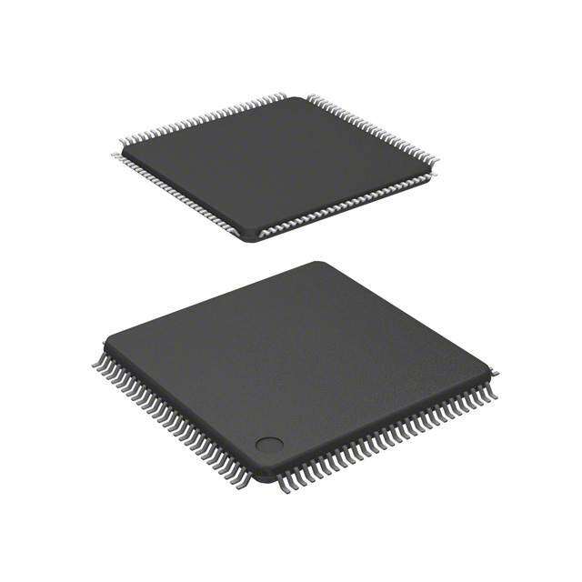
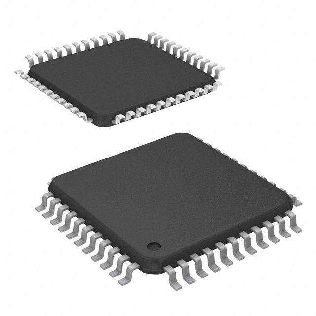
ICGOO电子元器件商城为您提供PIC18F4321-I/PT由Microchip设计生产,在icgoo商城现货销售,并且可以通过原厂、代理商等渠道进行代购。 PIC18F4321-I/PT价格参考。MicrochipPIC18F4321-I/PT封装/规格:嵌入式 - 微控制器, PIC 微控制器 IC PIC® 18F 8-位 40MHz 8KB(4K x 16) 闪存 44-TQFP(10x10)。您可以下载PIC18F4321-I/PT参考资料、Datasheet数据手册功能说明书,资料中有PIC18F4321-I/PT 详细功能的应用电路图电压和使用方法及教程。
Microchip Technology的PIC18F4321-I/PT是一款基于8位架构的嵌入式微控制器,适用于多种应用场景。这款微控制器具有丰富的外设和功能,能够满足工业控制、消费电子、汽车电子等多个领域的需求。

 1. 工业自动化
PIC18F4321-I/PT在工业自动化中的应用非常广泛。它可以通过其内置的ADC(模数转换器)和PWM(脉宽调制)模块实现对传感器数据的采集和电机控制。例如,在工厂生产线中,它可以用于监控温度、湿度等环境参数,并通过控制继电器或伺服电机来调节设备运行状态。此外,它还支持UART、SPI、I²C等多种通信接口,方便与上位机或其他设备进行数据交换,实现远程监控和管理。

 2. 消费电子产品
在消费电子产品中,PIC18F4321-I/PT可以用于智能家居设备、家电控制器等。例如,在智能灯控系统中,它可以通过红外接收器或无线模块接收用户指令,控制灯光的开关、亮度调节等功能。其低功耗特性使得它非常适合电池供电的产品,如便携式电子设备。同时,该微控制器的高集成度和灵活性也使其能够轻松应对各种复杂的用户交互需求。

 3. 汽车电子
在汽车电子领域,PIC18F4321-I/PT可用于车身控制模块(BCM)、仪表盘显示控制等。它可以实时监测车辆的各种状态信息,如油量、水温、胎压等,并将这些信息显示给驾驶员。此外,它还可以与其他车载系统通过CAN总线进行通信,确保整个车辆系统的协调工作。

 4. 医疗设备
在医疗设备方面,PIC18F4321-I/PT可以应用于血糖仪、血压计等小型便携式医疗仪器。它能够精确地处理传感器数据,并通过LCD显示屏为用户提供直观的结果。其可靠性和稳定性保证了医疗设备的安全性和准确性。

总之,PIC18F4321-I/PT凭借其强大的性能和灵活的配置,可以在多个行业中找到广泛的应用场景。
| 参数 | 数值 |
| A/D位大小 | 10 bit |
| 产品目录 | 集成电路 (IC)半导体 |
| 描述 | IC MCU 8BIT 8KB FLASH 44TQFP8位微控制器 -MCU 8 KB Flash 512 RAM |
| EEPROM容量 | 256 x 8 |
| 产品分类 | |
| I/O数 | 36 |
| 品牌 | Microchip Technology |
| 产品手册 | |
| 产品图片 |
|
| rohs | 符合RoHS无铅 / 符合限制有害物质指令(RoHS)规范要求 |
| 产品系列 | 嵌入式处理器和控制器,微控制器 - MCU,8位微控制器 -MCU,Microchip Technology PIC18F4321-I/PTPIC® 18F |
| 数据手册 | http://www.microchip.com/mymicrochip/filehandler.aspx?ddocname=en544918http://www.microchip.com/mymicrochip/filehandler.aspx?ddocname=en027611http://www.microchip.com/mymicrochip/filehandler.aspx?ddocname=en528369http://www.microchip.com/mymicrochip/filehandler.aspx?ddocname=en531149http://www.microchip.com/mymicrochip/filehandler.aspx?ddocname=en012514 |
| 产品型号 | PIC18F4321-I/PT |
| PCN组件/产地 | http://www.microchip.com/mymicrochip/NotificationDetails.aspx?id=5528&print=viewhttp://www.microchip.com/mymicrochip/NotificationDetails.aspx?id=5968&print=viewhttp://www.microchip.com/mymicrochip/NotificationDetails.aspx?pcn=IIRA-22KPRZ871&print=view |
| PCN设计/规格 | http://www.microchip.com/mymicrochip/NotificationDetails.aspx?id=5698&print=viewhttp://www.microchip.com/mymicrochip/NotificationDetails.aspx?pcn=SYST-06PGWI506&print=view |
| RAM容量 | 512 x 8 |
| 产品培训模块 | http://www.digikey.cn/PTM/IndividualPTM.page?site=cn&lang=zhs&ptm=2046http://www.digikey.cn/PTM/IndividualPTM.page?site=cn&lang=zhs&ptm=25053 |
| 产品目录页面 | |
| 产品种类 | 8位微控制器 -MCU |
| 供应商器件封装 | 44-TQFP(10x10) |
| 其它名称 | PIC18F4321IPT |
| 包装 | 托盘 |
| 可用A/D通道 | 13 |
| 可编程输入/输出端数量 | 36 |
| 商标 | Microchip Technology |
| 处理器系列 | PIC18 |
| 外设 | 欠压检测/复位,HLVD,POR,PWM,WDT |
| 安装风格 | SMD/SMT |
| 定时器数量 | 4 Timer |
| 封装 | Tray |
| 封装/外壳 | 44-TQFP |
| 封装/箱体 | TQFP-44 |
| 工作温度 | -40°C ~ 85°C |
| 工作电源电压 | 2 V to 5.5 V |
| 工厂包装数量 | 160 |
| 振荡器类型 | 内部 |
| 接口类型 | EUSART, I2C, MSSP, SPI |
| 数据RAM大小 | 512 B |
| 数据Ram类型 | RAM |
| 数据总线宽度 | 8 bit |
| 数据转换器 | A/D 13x10b |
| 最大工作温度 | + 125 C |
| 最大时钟频率 | 40 MHz |
| 最小工作温度 | - 40 C |
| 标准包装 | 160 |
| 核心 | PIC |
| 核心处理器 | PIC |
| 核心尺寸 | 8-位 |
| 片上ADC | Yes |
| 电压-电源(Vcc/Vdd) | 4.2 V ~ 5.5 V |
| 电源电压-最大 | 5.5 V |
| 电源电压-最小 | 4.2 V |
| 程序存储器大小 | 8 kB |
| 程序存储器类型 | Flash |
| 程序存储容量 | 8KB(4K x 16) |
| 系列 | PIC18 |
| 输入/输出端数量 | 36 I/O |
| 连接性 | I²C, SPI, UART/USART |
| 速度 | 40MHz |
| 配用 | /product-detail/zh/AC164305/AC164305-ND/613139/product-detail/zh/LABX1A/444-1001-ND/500789/product-detail/zh/AC164020/AC164020-ND/273319 |


- 商务部:美国ITC正式对集成电路等产品启动337调查
- 曝三星4nm工艺存在良率问题 高通将骁龙8 Gen1或转产台积电
- 太阳诱电将投资9.5亿元在常州建新厂生产MLCC 预计2023年完工
- 英特尔发布欧洲新工厂建设计划 深化IDM 2.0 战略
- 台积电先进制程称霸业界 有大客户加持明年业绩稳了
- 达到5530亿美元!SIA预计今年全球半导体销售额将创下新高
- 英特尔拟将自动驾驶子公司Mobileye上市 估值或超500亿美元
- 三星加码芯片和SET,合并消费电子和移动部门,撤换高东真等 CEO
- 三星电子宣布重大人事变动 还合并消费电子和移动部门
- 海关总署:前11个月进口集成电路产品价值2.52万亿元 增长14.8%


PDF Datasheet 数据手册内容提取
PIC18F2XXX/4XXX FAMILY Flash Microcontroller Programming Specification 1.0 DEVICE OVERVIEW This document includes the programming specifications for the following devices: • PIC18F2221 • PIC18F2580 • PIC18F4480 • PIC18F2321 • PIC18F2585 • PIC18F4510 • PIC18F2410 • PIC18F2610 • PIC18F4515 • PIC18F2420 • PIC18F2620 • PIC18F4520 • PIC18F2423 • PIC18F2680 • PIC18F4523 • PIC18F2450 • PIC18F2682 • PIC18F4525 • PIC18F2455 • PIC18F2685 • PIC18F4550 • PIC18F2458 • PIC18F4221 • PIC18F4553 • PIC18F2480 • PIC18F4321 • PIC18F4580 • PIC18F2510 • PIC18F4410 • PIC18F4585 • PIC18F2515 • PIC18F4420 • PIC18F4610 • PIC18F2520 • PIC18F4423 • PIC18F4620 • PIC18F2523 • PIC18F4450 • PIC18F4680 • PIC18F2525 • PIC18F4455 • PIC18F4682 • PIC18F2550 • PIC18F4458 • PIC18F4685 • PIC18F2553 2.0 PROGRAMMING OVERVIEW PIC18F2XXX/4XXX Family devices can be programmed using either the high-voltage In-Circuit Serial Programming™ (ICSP™) method or the low-voltage ICSP method. Both methods can be done with the device in the user’s system. The low-voltage ICSP method is slightly different than the high-voltage method and these differences are noted where applicable. This programming specification applies to the PIC18F2XXX/4XXX Family devices in all package types. 2.1 Hardware Requirements In High-Voltage ICSP mode, PIC18F2XXX/4XXX Family devices require two programmable power supplies: one for VDD and one for MCLR/VPP/RE3. Both supplies should have a minimum resolution of 0.25V. Refer to Section 6.0 “AC/ DC Characteristics Timing Requirements for Program/Verify Test Mode” for additional hardware parameters. 2.1.1 LOW-VOLTAGE ICSP PROGRAMMING In Low-Voltage ICSP mode, PIC18F2XXX/4XXX Family devices can be programmed using a VDD source in the operating range. The MCLR/VPP/RE3 does not have to be brought to a different voltage, but can instead be left at the normal operating voltage. Refer to Section 6.0 “AC/DC Characteristics Timing Requirements for Program/Verify Test Mode” for additional hardware parameters. 2.2 Pin Diagrams The pin diagrams for the PIC18F2XXX/4XXX Family are shown in Figure 2-1, Figure 2-2, Figure 2-3, Figure 2-4, Figure 2-5. 2010-2015 Microchip Technology Inc. DS30009622M-page 1
PIC18F2XXX/4XXX FAMILY TABLE 2-1: PIN DESCRIPTIONS (DURING PROGRAMMING): PIC18F2XXX/4XXX FAMILY During Programming Pin Name Pin Name Pin Type Pin Description MCLR/VPP/RE3 VPP P Programming Enable VDD(2) VDD P Power Supply VSS(2) VSS P Ground RB5 PGM I Low-Voltage ICSP™ Input when LVP Configuration bit equals ‘1’(1) RB6 PGC I Serial Clock RB7 PGD I/O Serial Data Legend: I = Input, O = Output, P = Power Note 1: See Figure 5-1 for more information. 2: All power supply (VDD) and ground (VSS) pins must be connected. The following devices are included in 28-pin SPDIP, PDIP and SOIC parts: • PIC18F2221 • PIC18F2480 • PIC18F2580 • PIC18F2321 • PIC18F2510 • PIC18F2585 • PIC18F2410 • PIC18F2515 • PIC18F2610 • PIC18F2420 • PIC18F2520 • PIC18F2620 • PIC18F2423 • PIC18F2523 • PIC18F2680 • PIC18F2450 • PIC18F2525 • PIC18F2682 • PIC18F2455 • PIC18F2550 • PIC18F2685 • PIC18F2458 • PIC18F2553 The following devices are included in 28-pin SSOP parts: • PIC18F2221 • PIC18F2321 FIGURE 2-1: 28-Pin SPDIP, PDIP, SOIC,SSOP MCLR/VPP/RE3 1 28 RB7/PGD RA0 2 27 RB6/PGC RA1 3 26 RB5/PGM RA2 4 25 RB4 RA3 5 X 24 RB3 X RA4 6 X 23 RB2 RA5 7 F2 22 RB1 VSS 8 18 21 RB0 OSC1 9 C 20 VDD OSC2 10 PI 19 VSS RC0 11 18 RC7 RC1 12 17 RC6 RC2 13 16 RC5 RC3 14 15 RC4 DS30009622M-page 2 2010-2015 Microchip Technology Inc.
PIC18F2XXX/4XXX FAMILY The following devices are included in 28-pin QFN parts: • PIC18F2221 • PIC18F2423 • PIC18F2510 • PIC18F2580 • PIC18F2321 • PIC18F2450 • PIC18F2520 • PIC18F2682 • PIC18F2410 • PIC18F2480 • PIC18F2523 • PIC18F2685 • PIC18F2420 • • • FIGURE 2-2: 28-Pin QFN 3 E R /PPDCM VGGG R/PPP A1A0 CLB7/B6/B5/B4 RR MRRRR 28272625242322 RA2 1 21 RB3 RA3 2 20 RB2 RA4 3 19 RB1 RA5 4 PIC18F2XXX 18 RB0 VSS 5 17 VDD OSC1 6 16 VSS OSC2 7 15 RC7 8 91011121314 0123456 CCCCCCC RRRRRRR The following devices are included in 40-pin PDIP parts: • PIC18F4221 • PIC18F4455 • PIC18F4523 • PIC18F4610 • PIC18F4321 • PIC18F4458 • PIC18F4525 • PIC18F4620 • PIC18F4410 • PIC18F4480 • PIC18F4550 • PIC18F4680 • PIC18F4420 • PIC18F4510 • PIC18F4553 • PIC18F4682 • PIC18F4423 • PIC18F4515 • PIC18F4580 • PIC18F4685 • PIC18F4450 • PIC18F4520 • PIC18F4585 • FIGURE 2-3: 40-Pin PDIP MCLR/VPP/RE3 1 40 RB7/PGD RA0 2 39 RB6/PGC RA1 3 38 RB5/PGM RA2 4 37 RB4 RA3 5 36 RB3 RA4 6 35 RB2 RA5 7 34 RB1 RE0 8 X 33 RB0 X RE1 9 X 32 VDD RE2 10 F4 31 VSS VDD 11 8 30 RD7 1 VSS 12 C 29 RD6 OSC1 13 PI 28 RD5 OSC2 14 27 RD4 RC0 15 26 RC7 RC1 16 25 RC6 RC2 17 24 RC5 RC3 18 23 RC4 RD0 19 22 RD3 RD1 20 21 RD2 2010-2015 Microchip Technology Inc. DS30009622M-page 3
PIC18F2XXX/4XXX FAMILY The following devices are included in 44-pin TQFP parts: • PIC18F4221 • PIC18F4523 • PIC18F4321 • PIC18F4525 • PIC18F4410 • PIC18F4550 • PIC18F4420 • PIC18F4553 • PIC18F4423 • PIC18F4580 • PIC18F4450 • PIC18F4585 • PIC18F4455 • PIC18F4610 • PIC18F4458 • PIC18F4620 • PIC18F4480 • PIC18F4680 • PIC18F4510 • PIC18F4682 • PIC18F4520 • PIC18F4685 • PIC18F4515 FIGURE 2-4: 44-PIN TQFP S T R O P C C6C5C4D3D2D1D0C3C2C1(1)C/I RRRRRRRRRRN 43210987654 RC7 14444433333333 NC(1)/ICVPP RD4 2 32 RC0 RD5 3 31 OSC2 RD6 4 30 OSC1 RD7 5 29 VSS VSS 6 PIC18F4XXX 28 VDD VDD 7 27 RE2 RB0 8 26 RE1 RB1 9 25 RE0 RB2 10 24 RA5 RB3 11 23 RA4 23456789012 11111111222 (1)C/ICPGC(1)C/ICPGDRB4RB5/PGMRB6/PGCRB7/PGDR/V/RE3PPRA0RA1RA2RA3 NN CL M Note 1: These pins are NC (No Connect) for all devices listed above with the exception of the PIC18F4450, PIC18F4455, PIC18F4458 and the PIC18F4553 devices (see Section 2.8 “Dedicated ICSP/ICD Port (44-Pin TQFP Only)” for more information on programming these pins in these devices). DS30009622M-page 4 2010-2015 Microchip Technology Inc.
PIC18F2XXX/4XXX FAMILY The following devices are included in 44-pin QFN parts: • PIC18F4221 • PIC18F4523 • PIC18F4321 • PIC18F4525 • PIC18F4410 • PIC18F4550 • PIC18F4420 • PIC18F4553 • PIC18F4423 • PIC18F4580 • PIC18F4450 • PIC18F4585 • PIC18F4455 • PIC18F4610 • PIC18F4458 • PIC18F4620 • PIC18F4480 • PIC18F4680 • PIC18F4510 • PIC18F4682 • PIC18F4520 • PIC18F4685 • PIC18F4515 FIGURE 2-5: 44-PIN QFN PM RC6D+/VD-/VRD3RD2RD1RD0VUSBRC2RC1RC0 43210987654 44444333333 RC7 1 33 OSC2 RD4 2 32 OSC1 RD5 3 31 VSS RD6 4 30 AVSS RD7 5 29 VDD VSS 6 PIC18F4XXX 28 AVDD AVDD 7 27 RE2 VDD 8 26 RE1 RB0 9 25 RE0 RB1 10 24 RA5 RB2 11 23 RA4 23456789012 11111111222 RB3NCRB4PGMPGCPGDRE3RA0RA1RA2RA3 RB5/RB6/RB7/R/V/PP L C M 2.3 Memory Maps For PIC18FX6X0 devices, the code memory space extends from 0000h to 0FFFFh (64 Kbytes) in four 16-Kbyte blocks. For PIC18FX5X5 devices, the code memory space extends from 0000h to 0BFFFFh (48 Kbytes) in three 16-Kbyte blocks. Addresses, 0000h through 07FFh, however, define a “Boot Block” region that is treated separately from Block 0. All of these blocks define code protection boundaries within the code memory space. The size of the Boot Block in PIC18F2585/2680/4585/4680 devices can be configured as 1, 2 or 4K words (see Figure 2-6). This is done through the BBSIZ<1:0> bits in the Configuration register, CONFIG4L. It is important to note that increasing the size of the Boot Block decreases the size of Block 0. 2010-2015 Microchip Technology Inc. DS30009622M-page 5
PIC18F2XXX/4XXX FAMILY TABLE 2-2: IMPLEMENTATION OF CODE MEMORY Device Code Memory Size (Bytes) PIC18F2515 PIC18F2525 PIC18F2585 000000h-00BFFFh (48K) PIC18F4515 PIC18F4525 PIC18F4585 PIC18F2610 PIC18F2620 PIC18F2680 000000h-00FFFFh (64K) PIC18F4610 PIC18F4620 PIC18F4680 FIGURE 2-6: MEMORY MAP AND THE CODE MEMORY SPACE FOR PIC18FX5X5/X6X0 DEVICES 000000h MEMORY SIZE/DEVICE Address Range Code Memory 01FFFFh 64 Kbytes 48 Kbytes (PIC18FX6X0) (PIC18FX5X5) BBSIZ<1:0> 11/10 01 00 11/10 01 00 000000h Boot Boot Unimplemented Read as ‘0’ Boot Block* Boot Block* 0007FFh Block* Block* 000800h Boot Boot Block* Block* 000FFFh 001000h Block 0 Block 0 001FFFh Block 0 002000h Block 0 200000h Block 0 Block 0 003FFFh 004000h Block 1 Block 1 Configuration 007FFFh 008000h and ID Space Block 2 Block 2 00BFFFh 00C000h Block 3 Unimplemented 00FFFFh Reads all ‘0’s Unimplemented 3FFFFFh Reads all ‘0’s 01FFFFh Note: Sizes of memory areas are not to scale. * Boot Block size is determined by the BBSIZ<1:0> bits in the CONFIG4L register. DS30009622M-page 6 2010-2015 Microchip Technology Inc.
PIC18F2XXX/4XXX FAMILY For PIC18F2685/4685 devices, the code memory space extends from 0000h to 017FFFh (96 Kbytes) in five 16-Kbyte blocks. For PIC18F2682/4682 devices, the code memory space extends from 0000h to 0013FFFh (80 Kbytes) in four 16-Kbyte blocks. Addresses, 0000h through 0FFFh, however, define a “Boot Block” region that is treated separately from Block 0. All of these blocks define code protection boundaries within the code memory space. The size of the Boot Block in PIC18F2685/4685 and PIC18F2682/4682 devices can be configured as 1, 2 or 4K words (see Figure 2-7). This is done through the BBSIZ<2:1> bits in the Configuration register, CONFIG4L. It is important to note that increasing the size of the Boot Block decreases the size of Block 0. TABLE 2-3: IMPLEMENTATION OF CODE MEMORY Device Code Memory Size (Bytes) PIC18F2682 000000h-013FFFh (80K) PIC18F4682 PIC18F2685 000000h-017FFFh (96K) PIC18F4685 2010-2015 Microchip Technology Inc. DS30009622M-page 7
PIC18F2XXX/4XXX FAMILY FIGURE 2-7: MEMORY MAP AND THE CODE MEMORY SPACE FOR PIC18F2685/4685 AND PIC18F2682/4682 DEVICES 000000h MEMORY SIZE/DEVICE Address Range Code Memory 96 Kbytes 80 Kbytes 01FFFFh (PIC18F2685/4685) (PIC18F2682/4682) BBSIZ1:BBSIZ2 11/10 01 00 11/10 01 00 000000h Boot Boot Boot Block* Boot Block* 0007FFh Unimplemented Block* Block* 000800h Boot Boot Read as ‘0’ Block* Block* 000FFFh 001000h Block 0 Block 0 001FFFh 002000h Block 0 Block 0 Block 0 Block 0 003FFFh 200000h 004000h Block 1 Block 1 007FFFh 008000h Block 2 Block 2 00BFFFh Configuration 00C000h and ID Block 3 Block 3 Space 00FFFFh 010000h Block 4 Block 4 013FFFh 014000h Block 5 Unimplemented 017FFFh Reads all ‘0’s Unimplemented Reads all ‘0’s 3FFFFFh 01FFFFh Note: Sizes of memory areas are not to scale. * Boot Block size is determined by the BBSIZ<1:2> bits in the CONFIG4L register. For PIC18FX5X0/X5X3 devices, the code memory space extends from 000000h to 007FFFh (32 Kbytes) in four 8-Kbyte blocks. For PIC18FX4X5/X4X8 devices, the code memory space extends from 000000h to 005FFFh (24 Kbytes) in three 8-Kbyte blocks. Addresses, 000000h through 0007FFh, however, define a “Boot Block” region that is treated separately from Block 0. All of these blocks define code protection boundaries within the code memory space. DS30009622M-page 8 2010-2015 Microchip Technology Inc.
PIC18F2XXX/4XXX FAMILY TABLE 2-4: IMPLEMENTATION OF CODE MEMORY Device Code Memory Size (Bytes) PIC18F2455 PIC18F2458 000000h-005FFFh (24K) PIC18F4455 PIC18F4458 PIC18F2510 PIC18F2520 PIC18F2523 PIC18F2550 PIC18F2553 000000h-007FFFh (32K) PIC18F4510 PIC18F4520 PIC18F4523 PIC18F4550 PIC18F4553 FIGURE 2-8: MEMORY MAP AND THE CODE MEMORY SPACE FOR PIC18FX4X5/X4X8/X5X0/X5X3 DEVICES 000000h Code Memory 1FFFFFh MEMORY SIZE/DEVICE 32 Kbytes 24 Kbytes Address (PIC18FX5X0/X5X3) (PIC18FX4X5/X4X8) Range 000000h Boot Block Boot Block 0007FFh Unimplemented Block 0 Block 0 000800h Read as ‘0’ 001FFFh 002000h Block 1 Block 1 003FFFh 004000h Block 2 Block 2 005FFFh 200000h 006000h Block 3 007FFFh 008000h Unimplemented Unimplemented Reads all ‘0’s 1FFFFFh Reads all ‘0’s Configuration and ID Space 3FFFFFh Note: Sizes of memory areas are not to scale. For PIC18FX4X0/X4X3 devices, the code memory space extends from 000000h to 003FFFh (16 Kbytes) in two 8-Kbyte blocks. Addresses, 000000h through 0003FFh, however, define a “Boot Block” region that is treated separately from Block 0. All of these blocks define code protection boundaries within the code memory space. 2010-2015 Microchip Technology Inc. DS30009622M-page 9
PIC18F2XXX/4XXX FAMILY TABLE 2-5: IMPLEMENTATION OF CODE MEMORY Device Code Memory Size (Bytes) PIC18F2410 PIC18F2420 PIC18F2423 PIC18F2450 000000h-003FFFh (16K) PIC18F4410 PIC18F4420 PIC18F4450 FIGURE 2-9: MEMORY MAP AND THE CODE MEMORY SPACE FOR PIC18FX4X0/X4X3 DEVICES 000000h Code Memory 1FFFFFh MEMORY SIZE/ DEVICE 16 Kbytes Address (PIC18FX4X0/X4X3) Range 000000h Boot Block 0007FFh Unimplemented 000800h Read as ‘0’ Block 0 001FFFh Block 1 002000h 003FFFh 004000h 005FFFh 200000h 006000h 007FFFh 008000h Unimplemented Reads all ‘0’s Configuration and ID Space 1FFFFFh 3FFFFFh Note: Sizes of memory areas are not to scale. For PIC18F2480/4480 devices, the code memory space extends from 0000h to 03FFFh (16 Kbytes) in one 16-Kbyte block. For PIC18F2580/4580 devices, the code memory space extends from 0000h to 07FFFh (32 Kbytes) in two 16-Kbyte blocks. Addresses, 0000h through 07FFh, however, define a “Boot Block” region that is treated separately from Block 0. All of these blocks define code protection boundaries within the code memory space. The size of the Boot Block in PIC18F2480/2580/4480/4580 devices can be configured as 1 or 2K words (see Figure 2-10). This is done through the BBSIZ<0> bit in the Configuration register, CONFIG4L. It is important to note that increasing the size of the Boot Block decreases the size of Block 0. DS30009622M-page 10 2010-2015 Microchip Technology Inc.
PIC18F2XXX/4XXX FAMILY TABLE 2-6: IMPLEMENTATION OF CODE MEMORY Device Code Memory Size (Bytes) PIC18F2480 000000h-003FFFh (16K) PIC18F4480 PIC18F2580 000000h-007FFFh (32K) PIC18F4580 FIGURE 2-10: MEMORY MAP AND THE CODE MEMORY SPACE FOR PIC18F2480/2580/4480/4580 DEVICES 000000h MEMORY SIZE/DEVICE Address Code Memory Range 01FFFFh 32 Kbytes 16 Kbytes (PIC18FX580) (PIC18FX480) BBSIZ<0> 1 0 1 0 Unimplemented 000000h Boot Block* Boot Block* Read as ‘0’ Boot Block* Boot Block* 0007FFh 000800h 000FFFh 001000h Block 0 Block 0 Block 0 Block 0 001FFFh 002000h 200000h Block 1 003FFFh 004000h Configuration and ID Space Block 2 005FFFh 006000h Block 3 Unimplemented Reads all ‘0’s 007FFFh 3FFFFFh Unimplemented Reads all ‘0’s 01FFFFh Note: Sizes of memory areas are not to scale. * Boot Block size is determined by the BBSIZ<0> bit in the CONFIG4L register. For PIC18F2221/4221 devices, the code memory space extends from 0000h to 00FFFh (4 Kbytes) in one 4-Kbyte block. For PIC18F2321/4321 devices, the code memory space extends from 0000h to 01FFFh (8 Kbytes) in two 4-Kbyte blocks. Addresses, 0000h through 07FFh, however, define a variable “Boot Block” region that is treated separately from Block 0. All of these blocks define code protection boundaries within the code memory space. 2010-2015 Microchip Technology Inc. DS30009622M-page 11
PIC18F2XXX/4XXX FAMILY The size of the Boot Block in PIC18F2221/2321/4221/4321 devices can be configured as 256, 512 or 1024 words (see Figure 2-11). This is done through the BBSIZ<1:0> bits in the Configuration register, CONFIG4L (see Figure 2-11). It is important to note that increasing the size of the Boot Block decreases the size of Block 0. TABLE 2-7: IMPLEMENTATION OF CODE MEMORY Device Code Memory Size (Bytes) PIC18F2221 000000h-000FFFh (4K) PIC18F4221 PIC18F2321 000000h-001FFFh (8K) PIC18F4321 FIGURE 2-11: MEMORY MAP AND THE CODE MEMORY SPACE FOR PIC18F2221/2321/4221/4321 DEVICES MEMORY SIZE/DEVICE Address Range 8 Kbytes 4 Kbytes 000000h (PIC18FX321) (PIC18FX221) Code Memory 01FFFFh BBSIZ<1:0> 11/10 01 00 11/10/01 00 000000h Boot Block* Boot Block* Boot Block* 256 words Boot Block* 256 words 0001FFh Unimplemented 512 words 512 words 000200h Read as ‘0’ Boot Block* 0003FFh 1K word Block 0 000400h Block 0 0.75K words 0.5K words 0007FFh Block 0 000800h 1.75K words Block 0 1.5K words 200000h Block 0 Block 1 1K word 1K word 000FFFh 001000h Configuration and ID Space Block 1 2K words Unimplemented Reads all ‘0’s 001FFFh 002000h Unimplemented 3FFFFFh Reads all ‘0’s 1FFFFFh Note: Sizes of memory areas are not to scale. * Boot Block size is determined by the BBSIZ<1:0> bits in the CONFIG4L register. DS30009622M-page 12 2010-2015 Microchip Technology Inc.
PIC18F2XXX/4XXX FAMILY In addition to the code memory space, there are three blocks that are accessible to the user through Table Reads and Table Writes. Their locations in the memory map are shown in Figure 2-12. Users may store identification information (ID) in eight ID registers. These ID registers are mapped in addresses, 200000h through 200007h. The ID locations read out normally, even after code protection is applied. Locations, 300000h through 30000Dh, are reserved for the Configuration bits. These bits select various device options and are described in Section 5.0 “Configuration Word”. These Configuration bits read out normally, even after code protection. Locations, 3FFFFEh and 3FFFFFh, are reserved for the Device ID bits. These bits may be used by the programmer to identify what device type is being programmed and are described in Section 5.0 “Configuration Word”. These Device ID bits read out normally, even after code protection. 2.3.1 MEMORY ADDRESS POINTER Memory in the address space, 0000000h to 3FFFFFh, is addressed via the Table Pointer register, which is comprised of three pointer registers: • TBLPTRU at RAM address 0FF8h • TBLPTRH at RAM address 0FF7h • TBLPTRL at RAM address 0FF6h TBLPTRU TBLPTRH TBLPTRL Addr[21:16] Addr[15:8] Addr[7:0] The 4-bit command, ‘0000’ (core instruction), is used to load the Table Pointer prior to using many read or write operations. 2010-2015 Microchip Technology Inc. DS30009622M-page 13
PIC18F2XXX/4XXX FAMILY FIGURE 2-12: CONFIGURATION AND ID LOCATIONS FOR PIC18F2XXX/4XXX FAMILY DEVICES 000000h Code Memory 01FFFFh ID Location 1 200000h ID Location 2 200001h ID Location 3 200002h ID Location 4 200003h ID Location 5 200004h ID Location 6 200005h ID Location 7 200006h Unimplemented ID Location 8 200007h Read as ‘0’ CONFIG1L 300000h CONFIG1H 300001h CONFIG2L 300002h CONFIG2H 300003h 1FFFFFh CONFIG3L 300004h CONFIG3H 300005h CONFIG4L 300006h Configuration CONFIG4H 300007h and ID CONFIG5L 300008h Space CONFIG5H 300009h CONFIG6L 30000Ah CONFIG6H 30000Bh 2FFFFFh CONFIG7L 30000Ch CONFIG7H 30000Dh Device ID1 3FFFFEh Device ID2 3FFFFFh 3FFFFFh Note: Sizes of memory areas are not to scale. DS30009622M-page 14 2010-2015 Microchip Technology Inc.
PIC18F2XXX/4XXX FAMILY 2.4 High-Level Overview of the Programming Process Figure 2-13 shows the high-level overview of the programming process. First, a Bulk Erase is performed. Next, the code memory, ID locations and data EEPROM are programmed (selected devices only, see Section 3.3 “Data EEPROM Programming”). These memories are then verified to ensure that programming was successful. If no errors are detected, the Configuration bits are then programmed and verified. FIGURE 2-13: HIGH-LEVEL PROGRAMMING FLOW Start Perform Bulk Erase Program Memory Program IDs Program Data EE(1) Verify Program Verify IDs Verify Data Program Configuration Bits Verify Configuration Bits Done Note 1: Selected devices only, see Section 3.3 “Data EEPROM Programming”. 2010-2015 Microchip Technology Inc. DS30009622M-page 15
PIC18F2XXX/4XXX FAMILY 2.5 Entering and Exiting High-Voltage ICSP Program/Verify Mode As shown in Figure 2-14, the High-Voltage ICSP Program/Verify mode is entered by holding PGC and PGD low and then raising MCLR/VPP/RE3 to VIHH (high voltage). Once in this mode, the code memory, data EEPROM (selected devices only, see Section 3.3 “Data EEPROM Programming”), ID locations and Configuration bits can be accessed and programmed in serial fashion. Figure 2-15 shows the exit sequence. The sequence that enters the device into the Program/Verify mode places all unused I/Os in the high-impedance state. FIGURE 2-14: ENTERING HIGH-VOLTAGE PROGRAM/VERIFY MODE P13 P12 P1 D110 MCLR/VPP/RE3 VDD PGD PGC PGD = Input FIGURE 2-15: EXITING HIGH-VOLTAGE PROGRAM/VERIFY MODE P16 P17 P1 MCLR/VPP/RE3 D110 VDD PGD PGC PGD = Input DS30009622M-page 16 2010-2015 Microchip Technology Inc.
PIC18F2XXX/4XXX FAMILY 2.6 Entering and Exiting Low-Voltage ICSP Program/Verify Mode When the LVP Configuration bit is ‘1’ (see Section 5.3 “Single-Supply ICSP Programming”), the Low-Voltage ICSP mode is enabled. As shown in Figure 2-16, Low-Voltage ICSP Program/Verify mode is entered by holding PGC and PGD low, placing a logic high on PGM and then raising MCLR/VPP/RE3 to VIH. In this mode, the RB5/PGM pin is dedicated to the programming function and ceases to be a general purpose I/O pin. Figure 2-17 shows the exit sequence. The sequence that enters the device into the Program/Verify mode places all unused I/Os in the high-impedance state. FIGURE 2-16: ENTERING LOW-VOLTAGE PROGRAM/VERIFY MODE P15 P12 VIH MCLR/VPP/RE3 VDD VIH PGM PGD PGC PGD = Input FIGURE 2-17: EXITING LOW-VOLTAGE PROGRAM/VERIFY MODE P16 P18 MCLR/VPP/RE3 VIH VDD PGM VIH PGD PGC PGD = Input 2010-2015 Microchip Technology Inc. DS30009622M-page 17
PIC18F2XXX/4XXX FAMILY 2.7 Serial Program/Verify Operation The PGC pin is used as a clock input pin and the PGD pin is used for entering command bits and data input/output during serial operation. Commands and data are transmitted on the rising edge of PGC, latched on the falling edge of PGC and are Least Significant bit (LSb) first. 2.7.1 4-BIT COMMANDS All instructions are 20 bits, consisting of a leading 4-bit command followed by a 16-bit operand, which depends on the type of command being executed. To input a command, PGC is cycled four times. The commands needed for programming and verification are shown in Table 2-8. Depending on the 4-bit command, the 16-bit operand represents 16 bits of input data or 8 bits of input data and 8 bits of output data. Throughout this specification, commands and data are presented as illustrated in Table 2-9. The 4-bit command is shown Most Significant bit (MSb) first. The command operand, or “Data Payload”, is shown as <MSB><LSB>. Figure 2-18 demonstrates how to serially present a 20-bit command/operand to the device. 2.7.2 CORE INSTRUCTION The core instruction passes a 16-bit instruction to the CPU core for execution. This is needed to set up registers as appropriate for use with other commands. TABLE 2-8: COMMANDS FOR PROGRAMMING Description 4-Bit Command Core Instruction 0000 (Shift in16-bit instruction) Shift Out TABLAT Register 0010 Table Read 1000 Table Read, Post-Increment 1001 Table Read, Post-Decrement 1010 Table Read, Pre-Increment 1011 Table Write 1100 Table Write, Post-Increment by 2 1101 Table Write, Start Programming, 1110 Post-Increment by 2 Table Write, Start Programming 1111 TABLE 2-9: SAMPLE COMMAND SEQUENCE 4-Bit Command Data Payload Core Instruction 1101 3C 40 Table Write, post-increment by 2 DS30009622M-page 18 2010-2015 Microchip Technology Inc.
PIC18F2XXX/4XXX FAMILY FIGURE 2-18: TABLE WRITE, POST-INCREMENT TIMING (1101) P2 P2A P2B 1 2 3 4 1 2 3 4 5 6 7 8 9 10 11 12 13 14 15 16 1 2 3 4 PGC P5 P5A P4 P3 PGD 1 0 1 1 0 0 0 0 0 0 1 0 0 0 1 1 1 1 0 0 n n n n 0 4 C 3 4-Bit Command 16-Bit Data Payload Fetch Next 4-Bit Command PGD = Input 2.8 Dedicated ICSP/ICD Port (44-Pin TQFP Only) The PIC18F4455/4458/4550/4553 44-pin TQFP devices are designed to support an alternate programming input: the dedicated ICSP/ICD port. The primary purpose of this port is to provide an alternate In-Circuit Debugging (ICD) option and free the pins (RB6, RB7 and MCLR) that would normally be used for debugging the application. In conjunction with ICD capability, however, the dedicated ICSP/ICD port also provides an alternate port for ICSP. Setting the ICPRT Configuration bit enables the dedicated ICSP/ICD port. The dedicated ICSP/ICD port functions the same as the default ICSP/ICD port; however, alternate pins are used instead of the default pins. Table 2-10 identifies the functionally equivalent pins for ICSP purposes: The dedicated ICSP/ICD port is an alternate port. Thus, ICSP is still available through the default port even though the ICPRT Configuration bit is set. When the VIH is seen on the MCLR/VPP/RE3 pin prior to applying VIH to the ICRST/ICVPP pin, then the state of the ICRST/ICVPP pin is ignored. Likewise, when the VIH is seen on ICRST/ICVPP prior to applying VIH to MCLR/VPP/RE3, then the state of the MCLR/VPP/RE3 pin is ignored. Note: The ICPRT Configuration bit can only be programmed through the default ICSP port. Chip Erase functions through the dedicated ICSP/ICD port do not affect this bit. When the ICPRT Configuration bit is set (dedicated ICSP/ICD port enabled), the NC/ICPORTS pin must be tied to either VDD or VSS. The ICPRT Configuration bit must be maintained clear for all 28-pin and 40-pin devices; otherwise, unexpected operation may occur. TABLE 2-10: ICSP™ EQUIVALENT PINS During Programming Pin Name Pin Name Pin Type Dedicated Pins Pin Description MCLR/VPP/RE3 VPP P NC/ICRST/ICVPP Programming Enable RB6 PGC I NC/ICCK/ICPGC Serial Clock RB7 PGD I/O NC/ICDT/ICPGD Serial Data Legend: I = Input, O = Output, P = Power 2010-2015 Microchip Technology Inc. DS30009622M-page 19
PIC18F2XXX/4XXX FAMILY 3.0 DEVICE PROGRAMMING Programming includes the ability to erase or write the various memory regions within the device. In all cases, except high-voltage ICSP Bulk Erase, the EECON1 register must be configured in order to operate on a particular memory region. When using the EECON1 register to act on code memory, the EEPGD bit must be set (EECON1<7> = 1) and the CFGS bit must be cleared (EECON1<6> = 0). The WREN bit must be set (EECON1<2> = 1) to enable writes of any sort (e.g., erases) and this must be done prior to initiating a write sequence. The FREE bit must be set (EECON1<4> = 1) in order to erase the program space being pointed to by the Table Pointer. The erase or write sequence is initiated by setting the WR bit (EECON1<1> = 1). It is strongly recommended that the WREN bit only be set immediately prior to a program erase. 3.1 ICSP Erase 3.1.1 HIGH-VOLTAGE ICSP BULK ERASE Erasing code or data EEPROM is accomplished by configuring two Bulk Erase Control registers located at 3C0004h and 3C0005h. Code memory may be erased, portions at a time, or the user may erase the entire device in one action. Bulk Erase operations will also clear any code-protect settings associated with the memory block being erased. Erase options are detailed in Table 3-1. If data EEPROM is code-protected (CPD = 0), the user must request an erase of data EEPROM (e.g., 0084h as shown in Table 3-1). TABLE 3-1: BULK ERASE OPTIONS Data Description (3C0005h:3C0004h) Chip Erase 3F8Fh Erase Data EEPROM(1) 0084h Erase Boot Block 0081h Erase Configuration Bits 0082h Erase Code EEPROM Block 0 0180h Erase Code EEPROM Block 1 0280h Erase Code EEPROM Block 2 0480h Erase Code EEPROM Block 3 0880h Erase Code EEPROM Block 4 1080h Erase Code EEPROM Block 5 2080h Note 1: Selected devices only, see Section 3.3 “Data EEPROM Programming”. The actual Bulk Erase function is a self-timed operation. Once the erase has started (falling edge of the 4th PGC after the NOP command), serial execution will cease until the erase completes (Parameter P11). During this time, PGC may continue to toggle but PGD must be held low. The code sequence to erase the entire device is shown in Table and the flowchart is shown in Figure 3-1. Note: A Bulk Erase is the only way to reprogram code-protect bits from an ON state to an OFF state. DS30009622M-page 20 2010-2015 Microchip Technology Inc.
PIC18F2XXX/4XXX FAMILY TABLE 3-2: BULK ERASE COMMAND SEQUENCE 4-Bit Command Data Payload Core Instruction 0000 0E 3C MOVLW 3Ch 0000 6E F8 MOVWF TBLPTRU 0000 0E 00 MOVLW 00h 0000 6E F7 MOVWF TBLPTRH 0000 0E 05 MOVLW 05h 0000 6E F6 MOVWF TBLPTRL 1100 3F 3F Write 3F3Fh to 3C0005h 0000 0E 3C MOVLW 3Ch 0000 6E F8 MOVWF TBLPTRU 0000 0E 00 MOVLW 00h 0000 6E F7 MOVWF TBLPTRH 0000 0E 04 MOVLW 04h 0000 6E F6 MOVWF TBLPTRL 1100 8F 8F Write 8F8Fh TO 3C0004h to erase entire device. NOP Hold PGD low until erase completes. 0000 00 00 0000 00 00 FIGURE 3-1: BULK ERASE FLOW Start Write 3F3Fh to 3C0005h Write 8F8Fh to 3C0004h to Erase Entire Device Delay P11 + P10 Time Done 2010-2015 Microchip Technology Inc. DS30009622M-page 21
PIC18F2XXX/4XXX FAMILY 3.1.2 LOW-VOLTAGE ICSP BULK ERASE When using low-voltage ICSP, the part must be supplied by the voltage specified in Parameter D111 if a Bulk Erase is to be executed. All other Bulk Erase details, as described above, apply. If it is determined that a program memory erase must be performed at a supply voltage below the Bulk Erase limit, refer to the erase methodology described in Section 3.1.3 “ICSP Row Erase” and Section 3.2.1 “Modifying Code Memory”. If it is determined that a data EEPROM erase (selected devices only, see Section 3.3 “Data EEPROM Programming”) must be performed at a supply voltage below the Bulk Erase limit, follow the methodology described in Section 3.3 “Data EEPROM Programming” and write ‘1’s to the array. FIGURE 3-2: BULK ERASE TIMING P10 1 2 3 4 1 2 15 16 1 2 3 4 1 2 15 16 1 2 3 4 1 2 PGC P5 P5A P5 P5A P11 PGD 0 0 1 1 1 1 0 0 0 0 0 0 0 0 0 0 0 0 0 0 n n 4-Bit Command 16-Bit 4-Bit Command 16-Bit 4-Bit Command Erase Time 16-Bit Data Payload Data Payload Data Payload PGD = Input 3.1.3 ICSP ROW ERASE Regardless of whether high or low-voltage ICSP is used, it is possible to erase one row (64 bytes of data), provided the block is not code or write-protected. Rows are located at static boundaries, beginning at program memory address, 000000h, extending to the internal program memory limit (see Section 2.3 “Memory Maps”). The Row Erase duration is externally timed and is controlled by PGC. After the WR bit in EECON1 is set, a NOP is issued, where the 4th PGC is held high for the duration of the programming time, P9. After PGC is brought low, the programming sequence is terminated. PGC must be held low for the time specified by Parameter P10 to allow high-voltage discharge of the memory array. The code sequence to Row Erase a PIC18F2XXX/4XXX Family device is shown in Table 3-3. The flowchart, shown in Figure 3-3, depicts the logic necessary to completely erase a PIC18F2XXX/4XXX Family device. The timing diagram that details the Start Programming command and Parameters P9 and P10 is shown in Figure 3-5. Note: The TBLPTR register can point to any byte within the row intended for erase. DS30009622M-page 22 2010-2015 Microchip Technology Inc.
PIC18F2XXX/4XXX FAMILY TABLE 3-3: ERASE CODE MEMORY CODE SEQUENCE 4-Bit Data Payload Core Instruction Command Step 1: Direct access to code memory and enable writes. 0000 8E A6 BSF EECON1, EEPGD 0000 9C A6 BCF EECON1, CFGS 0000 84 A6 BSF EECON1, WREN Step 2: Point to first row in code memory. 0000 6A F8 CLRF TBLPTRU 0000 6A F7 CLRF TBLPTRH 0000 6A F6 CLRF TBLPTRL Step 3: Enable erase and erase single row. 0000 88 A6 BSF EECON1, FREE 0000 82 A6 BSF EECON1, WR 0000 00 00 NOP – hold PGC high for time P9 and low for time P10. Step 4: Repeat Step 3, with the Address Pointer incremented by 64 until all rows are erased. FIGURE 3-3: SINGLE ROW ERASE CODE MEMORY FLOW Start Addr = 0 Configure Device for Row Erases Start Erase Sequence and Hold PGC High for Time P9 Addr = Addr + 64 Hold PGC Low for Time P10 All No rows done? Yes Done 2010-2015 Microchip Technology Inc. DS30009622M-page 23
PIC18F2XXX/4XXX FAMILY 3.2 Code Memory Programming Programming code memory is accomplished by first loading data into the write buffer and then initiating a programming sequence. The write and erase buffer sizes, shown in Table 3-4, can be mapped to any location of the same size, beginning at 000000h. The actual memory write sequence takes the contents of this buffer and programs the proper amount of code memory that contains the Table Pointer. The programming duration is externally timed and is controlled by PGC. After a Start Programming command is issued (4-bit command, ‘1111’), a NOP is issued, where the 4th PGC is held high for the duration of the programming time, P9. After PGC is brought low, the programming sequence is terminated. PGC must be held low for the time specified by Parameter P10 to allow high-voltage discharge of the memory array. The code sequence to program a PIC18F2XXX/4XXX Family device is shown in Table 3-5. The flowchart, shown in Figure 3-4, depicts the logic necessary to completely write a PIC18F2XXX/4XXX Family device. The timing diagram that details the Start Programming command and Parameters P9 and P10 is shown in Figure 3-5. Note: The TBLPTR register must point to the same region when initiating the programming sequence as it did when the write buffers were loaded. TABLE 3-4: WRITE AND ERASE BUFFER SIZES Devices (Arranged by Family) Write Buffer Size (Bytes) Erase Buffer Size (Bytes) PIC18F2221, PIC18F2321, PIC18F4221, PIC18F4321 8 64 PIC18F2450, PIC18F4450 16 64 PIC18F2410, PIC18F2510, PIC18F4410, PIC18F4510 PIC18F2420, PIC18F2520, PIC18F4420, PIC18F4520 PIC18F2423, PIC18F2523, PIC18F4423, PIC18F4523 32 64 PIC18F2480, PIC18F2580, PIC18F4480, PIC18F4580 PIC18F2455, PIC18F2550, PIC18F4455, PIC18F4550 PIC18F2458, PIC18F2553, PIC18F4458, PIC18F4553 PIC18F2515, PIC18F2610, PIC18F4515, PIC18F4610 PIC18F2525, PIC18F2620, PIC18F4525, PIC18F4620 64 64 PIC18F2585, PIC18F2680, PIC18F4585, PIC18F4680 PIC18F2682, PIC18F2685, PIC18F4682, PIC18F4685 DS30009622M-page 24 2010-2015 Microchip Technology Inc.
PIC18F2XXX/4XXX FAMILY TABLE 3-5: WRITE CODE MEMORY CODE SEQUENCE 4-Bit Data Payload Core Instruction Command Step 1: Direct access to code memory and enable writes. 0000 8E A6 BSF EECON1, EEPGD 0000 9C A6 BCF EECON1, CFGS Step 2: Load write buffer. 0000 0E <Addr[21:16]> MOVLW <Addr[21:16]> 0000 6E F8 MOVWF TBLPTRU 0000 0E <Addr[15:8]> MOVLW <Addr[15:8]> 0000 6E F7 MOVWF TBLPTRH 0000 0E <Addr[7:0]> MOVLW <Addr[7:0]> 0000 6E F6 MOVWF TBLPTRL Step 3: Repeat for all but the last two bytes. 1101 <MSB><LSB> Write 2 bytes and post-increment address by 2. Step 4: Load write buffer for last two bytes. 1111 <MSB><LSB> Write 2 bytes and start programming. 0000 00 00 NOP - hold PGC high for time P9 and low for time P10. To continue writing data, repeat Steps 2 through 4, where the Address Pointer is incremented by 2 at each iteration of the loop. 2010-2015 Microchip Technology Inc. DS30009622M-page 25
PIC18F2XXX/4XXX FAMILY FIGURE 3-4: PROGRAM CODE MEMORY FLOW Start N = 1 LoopCount = 0 Configure Device for Writes Load 2 Bytes N = N + 1 to Write Buffer at <Addr> All No bytes written? Yes N = 1 LoopCount = Start Write Sequence LoopCount + 1 and Hold PGC High until Done and Wait P9 Hold PGC Low for Time P10 No All locations done? Yes Done FIGURE 3-5: TABLE WRITE AND START PROGRAMMING INSTRUCTION TIMING (1111) P10 1 2 3 4 1 2 3 4 5 6 15 16 1 2 3 4 1 2 3 PGC P9 P5 P5A PGD 1 1 1 1 n n n n n n n n 0 0 0 0 0 0 0 4-Bit Command 16-Bit Data Payload 4-Bit Command Programming Time 16-Bit Data Payload PGD = Input DS30009622M-page 26 2010-2015 Microchip Technology Inc.
PIC18F2XXX/4XXX FAMILY 3.2.1 MODIFYING CODE MEMORY The previous programming example assumed that the device had been Bulk Erased prior to programming (see Section 3.1.1 “High-Voltage ICSP Bulk Erase”). It may be the case, however, that the user wishes to modify only a section of an already programmed device. The appropriate number of bytes required for the erase buffer must be read out of code memory (as described in Section 4.2 “Verify Code Memory and ID Locations”) and buffered. Modifications can be made on this buffer. Then, the block of code memory that was read out must be erased and rewritten with the modified data. The WREN bit must be set if the WR bit in EECON1 is used to initiate a write sequence. TABLE 3-6: MODIFYING CODE MEMORY 4-Bit Data Payload Core Instruction Command Step 1: Direct access to code memory. Step 2: Read and modify code memory (see Section 4.1 “Read Code Memory, ID Locations and Configuration Bits”). 0000 8E A6 BSF EECON1, EEPGD 0000 9C A6 BCF EECON1, CFGS Step 3: Set the Table Pointer for the block to be erased. 0000 0E <Addr[21:16]> MOVLW <Addr[21:16]> 0000 6E F8 MOVWF TBLPTRU 0000 0E <Addr[8:15]> MOVLW <Addr[8:15]> 0000 6E F7 MOVWF TBLPTRH 0000 0E <Addr[7:0]> MOVLW <Addr[7:0]> 0000 6E F6 MOVWF TBLPTRL Step 4: Enable memory writes and set up an erase. 0000 84 A6 BSF EECON1, WREN 0000 88 A6 BSF EECON1, FREE Step 5: Initiate erase. 0000 82 A6 BSF EECON1, WR 0000 00 00 NOP - hold PGC high for time P9 and low for time P10. Step 6: Load write buffer. The correct bytes will be selected based on the Table Pointer. 0000 0E <Addr[21:16]> MOVLW <Addr[21:16]> 0000 6E F8 MOVWF TBLPTRU 0000 0E <Addr[8:15]> MOVLW <Addr[8:15]> 0000 6E F7 MOVWF TBLPTRH 0000 0E <Addr[7:0]> MOVLW <Addr[7:0]> 0000 6E F6 MOVWF TBLPTRL 1101 <MSB><LSB> Write 2 bytes and post-increment address by 2. . . . . Repeat as many times as necessary to fill the write buffer . . 1111 <MSB><LSB> Write 2 bytes and start programming. 0000 00 00 NOP - hold PGC high for time P9 and low for time P10. To continue modifying data, repeat Steps 2 through 6, where the Address Pointer is incremented by the appropriate number of bytes (see Table 3-4) at each iteration of the loop. The write cycle must be repeated enough times to completely rewrite the contents of the erase buffer. Step 7: Disable writes. 0000 94 A6 BCF EECON1, WREN 2010-2015 Microchip Technology Inc. DS30009622M-page 27
PIC18F2XXX/4XXX FAMILY 3.3 Data EEPROM Programming Note: Data EEPROM programming is not available on the following devices: PIC18F2410 PIC18F4410 PIC18F2450 PIC18F4450 PIC18F2510 PIC18F4510 PIC18F2515 PIC18F4515 PIC18F2610 PIC18F4610 Data EEPROM is accessed one byte at a time via an Address Pointer (register pair: EEADRH:EEADR) and a data latch (EEDATA). Data EEPROM is written by loading EEADRH:EEADR with the desired memory location, EEDATA, with the data to be written and initiating a memory write by appropriately configuring the EECON1 register. A byte write automatically erases the location and writes the new data (erase-before-write). When using the EECON1 register to perform a data EEPROM write, both the EEPGD and CFGS bits must be cleared (EECON1<7:6> = 00). The WREN bit must be set (EECON1<2> = 1) to enable writes of any sort and this must be done prior to initiating a write sequence. The write sequence is initiated by setting the WR bit (EECON1<1> = 1). The write begins on the falling edge of the 4th PGC after the WR bit is set. It ends when the WR bit is cleared by hardware. After the programming sequence terminates, PGC must still be held low for the time specified by Parameter P10 to allow high-voltage discharge of the memory array. FIGURE 3-6: PROGRAM DATA FLOW Start Set Address Set Data Enable Write Start Write Sequence WR bit No clear? Yes No Done? Yes Done DS30009622M-page 28 2010-2015 Microchip Technology Inc.
PIC18F2XXX/4XXX FAMILY FIGURE 3-7: DATA EEPROM WRITE TIMING P10 1 2 3 4 1 2 15 16 1 2 PGC P5 P5A P11A PGD 0 0 0 0 n n 4-Bit Command BSF EECON1, WR Poll WR bit, Repeat until Clear 16-Bit Data (see below) Payload PGD = Input 1 2 3 4 1 2 15 16 1 2 3 4 1 2 15 16 PGC P5 P5A P5 P5A Poll WR bit PGD 0 0 0 0 0 0 0 0 4-Bit Command MOVF EECON1, W, 0 4-Bit Command MOVWF TABLAT Shift Out Data (see Figure 4-4) PGD = Input PGD = Output 2010-2015 Microchip Technology Inc. DS30009622M-page 29
PIC18F2XXX/4XXX FAMILY TABLE 3-7: PROGRAMMING DATA MEMORY 4-Bit Data Payload Core Instruction Command Step 1: Direct access to data EEPROM. 0000 9E A6 BCF EECON1, EEPGD 0000 9C A6 BCF EECON1, CFGS Step 2: Set the data EEPROM Address Pointer. 0000 0E <Addr> MOVLW <Addr> 0000 6E A9 MOVWF EEADR 0000 OE <AddrH> MOVLW <AddrH> 0000 6E AA MOVWF EEADRH Step 3: Load the data to be written. 0000 0E <Data> MOVLW <Data> 0000 6E A8 MOVWF EEDATA Step 4: Enable memory writes. 0000 84 A6 BSF EECON1, WREN Step 5: Initiate write. 0000 82 A6 BSF EECON1, WR Step 6: Poll WR bit, repeat until the bit is clear. 0000 50 A6 MOVF EECON1, W, 0 0000 6E F5 MOVWF TABLAT 0000 00 00 NOP 0010 <MSB><LSB> Shift out data(1) Step 7: Hold PGC low for time P10. Step 8: Disable writes. 0000 94 A6 BCF EECON1, WREN Repeat Steps 2 through 8 to write more data. Note 1: See Figure 4-4 for details on shift out data timing. DS30009622M-page 30 2010-2015 Microchip Technology Inc.
PIC18F2XXX/4XXX FAMILY 3.4 ID Location Programming The ID locations are programmed much like the code memory. The ID registers are mapped in addresses, 200000h through 200007h. These locations read out normally even after code protection. Note: The user only needs to fill the first 8 bytes of the write buffer in order to write the ID locations. Table 3-8 demonstrates the code sequence required to write the ID locations. In order to modify the ID locations, refer to the methodology described in Section 3.2.1 “Modifying Code Memory”. As with code memory, the ID locations must be erased before being modified. TABLE 3-8: WRITE ID SEQUENCE 4-Bit Data Payload Core Instruction Command Step 1: Direct access to code memory and enable writes. 0000 8E A6 BSF EECON1, EEPGD 0000 9C A6 BCF EECON1, CFGS Step 2: Load write buffer with 8 bytes and write. 0000 0E 20 MOVLW 20h 0000 6E F8 MOVWF TBLPTRU 0000 0E 00 MOVLW 00h 0000 6E F7 MOVWF TBLPTRH 0000 0E 00 MOVLW 00h 0000 6E F6 MOVWF TBLPTRL 1101 <MSB><LSB> Write 2 bytes and post-increment address by 2. 1101 <MSB><LSB> Write 2 bytes and post-increment address by 2. 1101 <MSB><LSB> Write 2 bytes and post-increment address by 2. 1111 <MSB><LSB> Write 2 bytes and start programming. 0000 00 00 NOP - hold PGC high for time P9 and low for time P10. 3.5 Boot Block Programming The code sequence detailed in Table 3-5 should be used, except that the address used in “Step 2” will be in the range of 000000h to 0007FFh. 3.6 Configuration Bits Programming Unlike code memory, the Configuration bits are programmed a byte at a time. The Table Write, Begin Programming 4-bit command (‘1111’) is used, but only eight bits of the following 16-bit payload will be written. The LSB of the payload will be written to even addresses and the MSB will be written to odd addresses. The code sequence to program two consecutive configuration locations is shown in Table 3-9. Note: The address must be explicitly written for each byte programmed. The addresses can not be incremented in this mode. 2010-2015 Microchip Technology Inc. DS30009622M-page 31
PIC18F2XXX/4XXX FAMILY TABLE 3-9: SET ADDRESS POINTER TO CONFIGURATION LOCATION 4-Bit Data Payload Core Instruction Command Step 1: Enable writes and direct access to configuration memory. 0000 8E A6 BSF EECON1, EEPGD 0000 8C A6 BSF EECON1, CFGS Step 2: Set Table Pointer for configuration byte to be written. Write even/odd addresses.(1) 0000 0E 30 MOVLW 30h 0000 6E F8 MOVWF TBLPTRU 0000 0E 00 MOVLW 00h 0000 6E F7 MOVWF TBLPRTH 0000 0E 00 MOVLW 00h 0000 6E F6 MOVWF TBLPTRL 1111 <MSB ignored><LSB> Load 2 bytes and start programming. 0000 00 00 NOP - hold PGC high for time P9 and low for time P10. 0000 0E 01 MOVLW 01h 0000 6E F6 MOVWF TBLPTRL 1111 <MSB><LSB ignored> Load 2 bytes and start programming. 0000 00 00 NOP - hold PGC high for time P9 and low for time P10. Note 1: Enabling the write protection of Configuration bits (WRTC = 0 in CONFIG6H) will prevent further writing of the Configuration bits. Always write all the Configuration bits before enabling the write protection for Configuration bits. FIGURE 3-8: CONFIGURATION PROGRAMMING FLOW Start Start Load Even Load Odd Configuration Configuration Address Address Program Program LSB MSB Delay P9 and P10 Delay P9 and P10 Time for Write Time for Write Done Done DS30009622M-page 32 2010-2015 Microchip Technology Inc.
PIC18F2XXX/4XXX FAMILY 4.0 READING THE DEVICE 4.1 Read Code Memory, ID Locations and Configuration Bits Code memory is accessed, one byte at a time, via the 4-bit command, ‘1001’ (Table Read, post-increment). The contents of memory pointed to by the Table Pointer (TBLPTRU:TBLPTRH:TBLPTRL) are serially output on PGD. The 4-bit command is shifted in, LSb first. The read is executed during the next eight clocks, then shifted out on PGD during the last eight clocks, LSb to MSb. A delay of P6 must be introduced after the falling edge of the 8th PGC of the operand to allow PGD to transition from an input to an output. During this time, PGC must be held low (see Figure 4-1). This operation also increments the Table Pointer by one, pointing to the next byte in code memory for the next read. This technique will work to read any memory in the 000000h to 3FFFFFh address space, so it also applies to the reading of the ID and Configuration registers. TABLE 4-1: READ CODE MEMORY SEQUENCE 4-Bit Data Payload Core Instruction Command Step 1: Set Table Pointer. 0000 0E <Addr[21:16]> MOVLW Addr[21:16] 0000 6E F8 MOVWF TBLPTRU 0000 0E <Addr[15:8]> MOVLW <Addr[15:8]> 0000 6E F7 MOVWF TBLPTRH 0000 0E <Addr[7:0]> MOVLW <Addr[7:0]> 0000 6E F6 MOVWF TBLPTRL Step 2: Read memory and then shift out on PGD, LSb to MSb. 1001 00 00 TBLRD *+ FIGURE 4-1: TABLE READ POST-INCREMENT INSTRUCTION TIMING (1001) 1 2 3 4 1 2 3 4 5 6 7 8 9 10 11 12 13 14 15 16 1 2 3 4 PGC P5 P6 P5A P14 PGD 1 0 0 1 LSb 1 2 3 4 5 6 MSb n n n n Shift Data Out Fetch Next 4-Bit Command PGD = Input PGD = Output PGD = Input 2010-2015 Microchip Technology Inc. DS30009622M-page 33
PIC18F2XXX/4XXX FAMILY 4.2 Verify Code Memory and ID Locations The verify step involves reading back the code memory space and comparing it against the copy held in the programmer’s buffer. Memory reads occur a single byte at a time, so two bytes must be read to compare against the word in the programmer’s buffer. Refer to Section 4.1 “Read Code Memory, ID Locations and Configuration Bits” for implementation details of reading code memory. The Table Pointer must be manually set to 200000h (base address of the ID locations) once the code memory has been verified. The post-increment feature of the Table Read 4-bit command may not be used to increment the Table Pointer beyond the code memory space. In a 64-Kbyte device, for example, a post-increment read of address, FFFFh, will wrap the Table Pointer back to 000000h, rather than point to the unimplemented address, 010000h. FIGURE 4-2: VERIFY CODE MEMORY FLOW Start Set TBLPTR = 0 Set TBLPTR = 200000h Read Low Byte Read Low Byte with Post-Increment with Post-Increment Read High Byte Increment Read High Byte with Post-Increment Pointer with Post-Increment Does Does No No Word = Expect Failure, Word = Expect Failure, Data? Report Data? Report Error Error Yes Yes All All No code memory No ID locations verified? verified? Yes Yes Done 4.3 Verify Configuration Bits A configuration address may be read and output on PGD via the 4-bit command, ‘1001’. Configuration data is read and written in a byte-wise fashion, so it is not necessary to merge two bytes into a word prior to a compare. The result may then be immediately compared to the appropriate configuration data in the programmer’s memory for verification. Refer to Section 4.1 “Read Code Memory, ID Locations and Configuration Bits” for implementation details of reading configuration data. DS30009622M-page 34 2010-2015 Microchip Technology Inc.
PIC18F2XXX/4XXX FAMILY 4.4 Read Data EEPROM Memory Data EEPROM is accessed, one byte at a time, via an Address Pointer (register pair: EEADRH:EEADR) and a data latch (EEDATA). Data EEPROM is read by loading EEADRH:EEADR with the desired memory location and initiating a memory read by appropriately configuring the EECON1 register. The data will be loaded into EEDATA, where it may be serially output on PGD via the 4-bit command, ‘0010’ (Shift Out Data Holding register). A delay of P6 must be introduced after the falling edge of the 8th PGC of the operand to allow PGD to transition from an input to an output. During this time, PGC must be held low (see Figure 4-4). The command sequence to read a single byte of data is shown in Table 4-2. FIGURE 4-3: READ DATA EEPROM FLOW Start Set Address Read Byte Move to TABLAT Shift Out Data No Done? Yes Done TABLE 4-2: READ DATA EEPROM MEMORY 4-Bit Data Payload Core Instruction Command Step 1: Direct access to data EEPROM. 0000 9E A6 BCF EECON1, EEPGD 0000 9C A6 BCF EECON1, CFGS Step 2: Set the data EEPROM Address Pointer. 0000 0E <Addr> MOVLW <Addr> 0000 6E A9 MOVWF EEADR 0000 OE <AddrH> MOVLW <AddrH> 0000 6E AA MOVWF EEADRH Step 3: Initiate a memory read. 0000 80 A6 BSF EECON1, RD Step 4: Load data into the Serial Data Holding register. 0000 50 A8 MOVF EEDATA, W, 0 0000 6E F5 MOVWF TABLAT 0000 00 00 NOP 0010 <MSB><LSB> Shift Out Data(1) Note 1: The <LSB> is undefined. The <MSB> is the data. 2010-2015 Microchip Technology Inc. DS30009622M-page 35
PIC18F2XXX/4XXX FAMILY FIGURE 4-4: SHIFT OUT DATA HOLDING REGISTER TIMING (0010) 1 2 3 4 1 2 3 4 5 6 7 8 9 10 11 12 13 14 15 16 1 2 3 4 PGC P5 P6 P5A P14 PGD 0 1 0 0 LSb 1 2 3 4 5 6 MSb n n n n Shift Data Out Fetch Next 4-Bit Command PGD = Input PGD = Output PGD = Input 4.5 Verify Data EEPROM A data EEPROM address may be read via a sequence of core instructions (4-bit command, ‘0000’) and then output on PGD via the 4-bit command, ‘0010’ (TABLAT register). The result may then be immediately compared to the appropriate data in the programmer’s memory for verification. Refer to Section 4.4 “Read Data EEPROM Memory” for implementation details of reading data EEPROM. 4.6 Blank Check The term Blank Check means to verify that the device has no programmed memory cells. All memories must be verified: code memory, data EEPROM, ID locations and Configuration bits. The Device ID registers (3FFFFEh:3FFFFFh) should be ignored. A “blank” or “erased” memory cell will read as ‘1’. Therefore, Blank Checking a device merely means to verify that all bytes read as FFh, except the Configuration bits. Unused (reserved) Configuration bits will read ‘0’ (programmed). Refer to Figure 4-5 for blank configuration expect data for the various PIC18F2XXX/4XXX Family devices. Given that Blank Checking is merely code and data EEPROM verification with FFh expect data, refer to Section 4.4 “Read Data EEPROM Memory” and Section 4.2 “Verify Code Memory and ID Locations” for implementation details. FIGURE 4-5: BLANK CHECK FLOW Start Blank Check Device Is Yes device Continue blank? No Abort DS30009622M-page 36 2010-2015 Microchip Technology Inc.
PIC18F2XXX/4XXX FAMILY 5.0 CONFIGURATION WORD The PIC18F2XXX/4XXX Family devices have several Configuration Words. These bits can be set or cleared to select various device configurations. All other memory areas should be programmed and verified prior to setting the Configuration Words. These bits may be read out normally, even after read or code protection. See Table 5-1 for a list of Configuration bits and Device IDs, and Table 5-3 for the Configuration bit descriptions. 5.1 ID Locations A user may store identification information (ID) in eight ID locations, mapped in 200000h:200007h. It is recommended that the Most Significant nibble of each ID be Fh. In doing so, if the user code inadvertently tries to execute from the ID space, the ID data will execute as a NOP. 5.2 Device ID Word The Device ID Word for the PIC18F2XXX/4XXX Family devices is located at 3FFFFEh:3FFFFFh. These bits may be used by the programmer to identify what device type is being programmed and read out normally, even after code or read protection. In some cases, devices may share the same DEVID values. In such cases, the Most Significant bit of the device revision, REV4 (DEVID1<4>), will need to be examined to completely determine the device being accessed. See Table 5-2 for a complete list of Device ID values. FIGURE 5-1: READ DEVICE ID WORD FLOW Start Set TBLPTR = 3FFFFE Read Low Byte with Post-Increment Read High Byte with Post-Increment Done 2010-2015 Microchip Technology Inc. DS30009622M-page 37
PIC18F2XXX/4XXX FAMILY TABLE 5-1: CONFIGURATION BITS AND DEVICE IDS Default/ File Name Bit 7 Bit 6 Bit 5 Bit 4 Bit 3 Bit 2 Bit 1 Bit 0 Unprogrammed Value 300000h(1,8) CONFIG1L — — USBDIV CPUDIV1 CPUDIV0 PLLDIV2 PLLDIV1 PLLDIV0 --00 0000 00-- 0111 300001h CONFIG1H IESO FCMEN — — FOSC3 FOSC2 FOSC1 FOSC0 00-- 0101(1,8) — ---1 1111 300002h CONFIG2L — — BORV1 BORV0 BOREN1 BOREN0 PWRTEN VREGEN(1,8) --01 1111(1,8) 300003h CONFIG2H — — — WDTPS3 WDTPS2 WDTPS1 WDTPS0 WDTEN ---1 1111 CCP2MX(7) 1--- -011(7) 300005h CONFIG3H MCLRE — — — — LPT1OSC PBADEN — 1--- -01- ICPRT(1) — — 100- -1-1(1) BBSIZ1 BBSIZ0 — 1000 -1-1 300006h CONFIG4L DEBUG XINST — BBSIZ(3) — LVP — STVREN 10-0 -1-1(3) ICPRT(8) — BBSIZ(8) 100- 01-1(8) BBSIZ1(2) BBSIZ2(2) — 1000 -1-1(2) 300008h CONFIG5L — — CP5(10) CP4(9) CP3(4) CP2(4) CP1 CP0 --11 1111 300009h CONFIG5H CPD CPB — — — — — — 11-- ---- 30000Ah CONFIG6L — — WRT5(10) WRT4(9) WRT3(4) WRT2(4) WRT1 WRT0 --11 1111 30000Bh CONFIG6H WRTD WRTB WRTC(5) — — — — — 111- ---- 30000Ch CONFIG7L — — EBTR5(10) EBTR4(9) EBTR3(4) EBTR2(4) EBTR1 EBTR0 --11 1111 30000Dh CONFIG7H — EBTRB — — — — — — -1-- ---- 3FFFFEh DEVID1(6) DEV2 DEV1 DEV0 REV4 REV3 REV2 REV1 REV0 See Table 5-2 3FFFFFh DEVID2(6) DEV10 DEV9 DEV8 DEV7 DEV6 DEV5 DEV4 DEV3 See Table 5-2 Legend: - = unimplemented. Shaded cells are unimplemented, read as ‘0’. Note 1: Implemented only on PIC18F2455/2550/4455/4550 and PIC18F2458/2553/4458/4553 devices. 2: Implemented on PIC18F2585/2680/4585/4680, PIC18F2682/2685 and PIC18F4682/4685 devices only. 3: Implemented on PIC18F2480/2580/4480/4580 devices only. 4: These bits are only implemented on specific devices based on available memory. Refer to Section 2.3 “Memory Maps”. 5: In PIC18F2480/2580/4480/4580 devices, this bit is read-only in Normal Execution mode; it can be written only in Program mode. 6: DEVID registers are read-only and cannot be programmed by the user. 7: Implemented on all devices with the exception of the PIC18FXX8X and PIC18F2450/4450 devices. 8: Implemented on PIC18F2450/4450 devices only. 9: Implemented on PIC18F2682/2685 and PIC18F4682/4685 devices only. 10: Implemented on PIC18F2685/4685 devices only. DS30009622M-page 38 2010-2015 Microchip Technology Inc.
PIC18F2XXX/4XXX FAMILY TABLE 5-2: DEVICE ID VALUES Device ID Value Device DEVID2 DEVID1 PIC18F2221 21h 011x xxxx PIC18F2321 21h 001x xxxx PIC18F2410 11h 011x xxxx PIC18F2420 11h 010x xxxx(1) PIC18F2423 11h 010x xxxx(2) PIC18F2450 24h 001x xxxx PIC18F2455 12h 011x xxxx PIC18F2458 2Ah 011x xxxx PIC18F2480 1Ah 111x xxxx PIC18F2510 11h 001x xxxx PIC18F2515 0Ch 111x xxxx PIC18F2520 11h 000x xxxx(1) PIC18F2523 11h 000x xxxx(2) PIC18F2525 0Ch 110x xxxx PIC18F2550 12h 010x xxxx PIC18F2553 2Ah 010x xxxx PIC18F2580 1Ah 110x xxxx PIC18F2585 0Eh 111x xxxx PIC18F2610 0Ch 101x xxxx PIC18F2620 0Ch 100x xxxx PIC18F2680 0Eh 110x xxxx PIC18F2682 27h 000x xxxx PIC18F2685 27h 001x xxxx PIC18F4221 21h 010x xxxx PIC18F4321 21h 000x xxxx PIC18F4410 10h 111x xxxx PIC18F4420 10h 110x xxxx(1) PIC18F4423 10h 110x xxxx(2) PIC18F4450 24h 000x xxxx PIC18F4455 12h 001x xxxx PIC18F4458 2Ah 001x xxxx PIC18F4480 1Ah 101x xxxx PIC18F4510 10h 101x xxxx PIC18F4515 0Ch 011x xxxx PIC18F4520 10h 100x xxxx(1) PIC18F4523 10h 100x xxxx(2) PIC18F4525 0Ch 010x xxxx PIC18F4550 12h 000x xxxx PIC18F4553 2Ah 000x xxxx PIC18F4580 1Ah 100x xxxx Legend: The ‘x’s in DEVID1 contain the device revision code. Note 1: DEVID1 bit 4 is used to determine the device type (REV4 = 0). 2: DEVID1 bit 4 is used to determine the device type (REV4 = 1). 2010-2015 Microchip Technology Inc. DS30009622M-page 39
PIC18F2XXX/4XXX FAMILY TABLE 5-2: DEVICE ID VALUES (CONTINUED) Device ID Value Device DEVID2 DEVID1 PIC18F4585 0Eh 101x xxxx PIC18F4610 0Ch 001x xxxx PIC18F4620 0Ch 000x xxxx PIC18F4680 0Eh 100x xxxx PIC18F4682 27h 010x xxxx PIC18F4685 27h 011x xxxx Legend: The ‘x’s in DEVID1 contain the device revision code. Note 1: DEVID1 bit 4 is used to determine the device type (REV4 = 0). 2: DEVID1 bit 4 is used to determine the device type (REV4 = 1). DS30009622M-page 40 2010-2015 Microchip Technology Inc.
PIC18F2XXX/4XXX FAMILY TABLE 5-3: PIC18F2XXX/4XXX FAMILY BIT DESCRIPTIONS Configuration Bit Name Description Words IESO CONFIG1H Internal External Switchover bit 1 = Internal External Switchover mode is enabled 0 = Internal External Switchover mode is disabled FCMEN CONFIG1H Fail-Safe Clock Monitor Enable bit 1 = Fail-Safe Clock Monitor is enabled 0 = Fail-Safe Clock Monitor is disabled FOSC<3:0> CONFIG1H Oscillator Selection bits 11xx = External RC oscillator, CLKO function on RA6 101x = External RC oscillator, CLKO function on RA6 1001 = Internal RC oscillator, CLKO function on RA6, port function on RA7 1000 = Internal RC oscillator, port function on RA6, port function on RA7 0111 = External RC oscillator, port function on RA6 0110 = HS oscillator, PLL is enabled (Clock Frequency = 4 x FOSC1) 0101 = EC oscillator, port function on RA6 0100 = EC oscillator, CLKO function on RA6 0011 = External RC oscillator, CLKO function on RA6 0010 = HS oscillator 0001 = XT oscillator 0000 = LP oscillator FOSC<3:0> CONFIG1H Oscillator Selection bits (PIC18F2455/2550/4455/4550, PIC18F2458/2553/4458/4553 and PIC18F2450/4450 devices only) 111x = HS oscillator, PLL is enabled, HS is used by USB 110x = HS oscillator, HS is used by USB 1011 = Internal oscillator, HS is used by USB 1010 = Internal oscillator, XT is used by USB 1001 = Internal oscillator, CLKO function on RA6, EC is used by USB 1000 = Internal oscillator, port function on RA6, EC is used by USB 0111 = EC oscillator, PLL is enabled, CLKO function on RA6, EC is used by USB 0110 = EC oscillator, PLL is enabled, port function on RA6, EC is used by USB 0101 = EC oscillator, CLKO function on RA6, EC is used by USB 0100 = EC oscillator, port function on RA6, EC is used by USB 001x = XT oscillator, PLL is enabled, XT is used by USB 000x = XT oscillator, XT is used by USB USBDIV CONFIG1L USB Clock Selection bit (PIC18F2455/2550/4455/4550, PIC18F2458/2553/4458/4553 and PIC18F2450/4450 devices only) Selects the clock source for full-speed USB operation: 1 = USB clock source comes from the 96 MHz PLL divided by 2 0 = USB clock source comes directly from the OSC1/OSC2 oscillator block; no divide CPUDIV<1:0> CONFIG1L CPU System Clock Selection bits (PIC18F2455/2550/4455/4550, PIC18F2458/2553/4458/4553 and PIC18F2450/4450 devices only) 11 = CPU system clock divided by 4 10 = CPU system clock divided by 3 01 = CPU system clock divided by 2 00 = No CPU system clock divide Note 1: The BBSIZ bits, BBSIZ<1:0> and BBSIZ<2:1> bits, cannot be changed once any of the following code-protect bits are enabled: CPB or CP0, WRTB or WRT0, EBTRB or EBTR0. 2: Not available in PIC18FXX8X and PIC18F2450/4450 devices. 2010-2015 Microchip Technology Inc. DS30009622M-page 41
PIC18F2XXX/4XXX FAMILY TABLE 5-3: PIC18F2XXX/4XXX FAMILY BIT DESCRIPTIONS (CONTINUED) Configuration Bit Name Description Words PLLDIV<2:0> CONFIG1L Oscillator Selection bits (PIC18F2455/2550/4455/4550, PIC18F2458/2553/4458/4553 and PIC18F2450/4450 devices only) Divider must be selected to provide a 4 MHz input into the 96 MHz PLL: 111 = Oscillator divided by 12 (48 MHz input) 110 = Oscillator divided by 10 (40 MHz input) 101 = Oscillator divided by 6 (24 MHz input) 100 = Oscillator divided by 5 (20 MHz input) 011 = Oscillator divided by 4 (16 MHz input) 010 = Oscillator divided by 3 (12 MHz input) 001 = Oscillator divided by 2 (8 MHz input) 000 = No divide – oscillator used directly (4 MHz input) VREGEN CONFIG2L USB Voltage Regulator Enable bit (PIC18F2455/2550/4455/4550, PIC18F2458/2553/4458/4553 and PIC18F2450/4450 devices only) 1 = USB voltage regulator is enabled 0 = USB voltage regulator is disabled BORV<1:0> CONFIG2L Brown-out Reset Voltage bits 11 = VBOR is set to 2.0V 10 = VBOR is set to 2.7V 01 = VBOR is set to 4.2V 00 = VBOR is set to 4.5V BOREN<1:0> CONFIG2L Brown-out Reset Enable bits 11 = Brown-out Reset is enabled in hardware only (SBOREN is disabled) 10 = Brown-out Reset is enabled in hardware only and disabled in Sleep mode SBOREN is disabled) 01 = Brown-out Reset is enabled and controlled by software (SBOREN is enabled) 00 = Brown-out Reset is disabled in hardware and software PWRTEN CONFIG2L Power-up Timer Enable bit 1 = PWRT is disabled 0 = PWRT is enabled WDPS<3:0> CONFIG2H Watchdog Timer Postscaler Select bits 1111 =1:32,768 1110 =1:16,384 1101 =1:8,192 1100 =1:4,096 1011 =1:2,048 1010 =1:1,024 1001 =1:512 1000 =1:256 0111 =1:128 0110 =1:64 0101 =1:32 0100 =1:16 0011 =1:8 0010 =1:4 0001 =1:2 0000 =1:1 Note 1: The BBSIZ bits, BBSIZ<1:0> and BBSIZ<2:1> bits, cannot be changed once any of the following code-protect bits are enabled: CPB or CP0, WRTB or WRT0, EBTRB or EBTR0. 2: Not available in PIC18FXX8X and PIC18F2450/4450 devices. DS30009622M-page 42 2010-2015 Microchip Technology Inc.
PIC18F2XXX/4XXX FAMILY TABLE 5-3: PIC18F2XXX/4XXX FAMILY BIT DESCRIPTIONS (CONTINUED) Configuration Bit Name Description Words WDTEN CONFIG2H Watchdog Timer Enable bit 1 = WDT is enabled 0 = WDT is disabled (control is placed on the SWDTEN bit) MCLRE CONFIG3H MCLR Pin Enable bit 1 = MCLR pin is enabled, RE3 input pin is disabled 0 = RE3 input pin is enabled, MCLR pin is disabled LPT1OSC CONFIG3H Low-Power Timer1 Oscillator Enable bit 1 = Timer1 is configured for low-power operation 0 = Timer1 is configured for high-power operation PBADEN CONFIG3H PORTB A/D Enable bit 1 = PORTB A/D<4:0> pins are configured as analog input channels on Reset 0 = PORTB A/D<4:0> pins are configured as digital I/O on Reset PBADEN CONFIG3H PORTB A/D Enable bit (PIC18FXX8X devices only) 1 = PORTB A/D<4:0> and PORTB A/D<1:0> pins are configured as analog input channels on Reset 0 = PORTB A/D<4:0> pins are configured as digital I/O on Reset CCP2MX CONFIG3H CCP2 MUX bit 1 = CCP2 input/output is multiplexed with RC1(2) 0 = CCP2 input/output is multiplexed with RB3 DEBUG CONFIG4L Background Debugger Enable bit 1 = Background debugger is disabled, RB6 and RB7 are configured as general purpose I/O pins 0 = Background debugger is enabled, RB6 and RB7 are dedicated to In-Circuit Debug XINST CONFIG4L Extended Instruction Set Enable bit 1 = Instruction set extension and Indexed Addressing mode are enabled 0 = Instruction set extension and Indexed Addressing mode are disabled (Legacy mode) ICPRT CONFIG4L Dedicated In-Circuit (ICD/ICSP™) Port Enable bit (PIC18F2455/2550/4455/4550, PIC18F2458/2553/4458/4553 and PIC18F2450/4450 devices only) 1 = ICPORT is enabled 0 = ICPORT is disabled BBSIZ<1:0>(1) CONFIG4L Boot Block Size Select bits (PIC18F2585/2680/4585/4680 devices only) 11 = 4K words (8 Kbytes) Boot Block 10 = 4K words (8 Kbytes) Boot Block 01 = 2K words (4 Kbytes) Boot Block 00 = 1K word (2 Kbytes) Boot Block BBSIZ<2:1>(1) CONFIG4L Boot Block Size Select bits (PIC18F2682/2685/4582/4685 devices only) 11 = 4K words (8 Kbytes) Boot Block 10 = 4K words (8 Kbytes) Boot Block 01 = 2K words (4 Kbytes) Boot Block 00 = 1K word (2 Kbytes) Boot Block Note 1: The BBSIZ bits, BBSIZ<1:0> and BBSIZ<2:1> bits, cannot be changed once any of the following code-protect bits are enabled: CPB or CP0, WRTB or WRT0, EBTRB or EBTR0. 2: Not available in PIC18FXX8X and PIC18F2450/4450 devices. 2010-2015 Microchip Technology Inc. DS30009622M-page 43
PIC18F2XXX/4XXX FAMILY TABLE 5-3: PIC18F2XXX/4XXX FAMILY BIT DESCRIPTIONS (CONTINUED) Configuration Bit Name Description Words BBSIZ<1:0>(1) CONFIG4L Boot Block Size Select bits (PIC18F2321/4321 devices only) 11 = 1K word (2 Kbytes) Boot Block 10 = 1K word (2 Kbytes) Boot Block 01 = 512 words (1 Kbyte) Boot Block 00 = 256 words (512 bytes) Boot Block Boot Block Size Select bits (PIC18F2221/4221 devices only) 11 = 512 words (1 Kbyte) Boot Block 10 = 512 words (1 Kbyte) Boot Block 01 = 512 words (1 Kbyte) Boot Block 00 = 256 words (512 bytes) Boot Block BBSIZ(1) CONFIG4L Boot Block Size Select bits (PIC18F2480/2580/4480/4580 and PIC18F2450/4450 devices only) 1 = 2K words (4 Kbytes) Boot Block 0 = 1K word (2 Kbytes) Boot Block LVP CONFIG4L Low-Voltage Programming Enable bit 1 = Low-Voltage Programming is enabled, RB5 is the PGM pin 0 = Low-Voltage Programming is disabled, RB5 is an I/O pin STVREN CONFIG4L Stack Overflow/Underflow Reset Enable bit 1 = Reset on stack overflow/underflow is enabled 0 = Reset on stack overflow/underflow is disabled CP5 CONFIG5L Code Protection bit (Block 5 code memory area) (PIC18F2685 and PIC18F4685 devices only) 1 = Block 5 is not code-protected 0 = Block 5 is code-protected CP4 CONFIG5L Code Protection bit (Block 4 code memory area) (PIC18F2682/2685 and PIC18F4682/4685 devices only) 1 = Block 4 is not code-protected 0 = Block 4 is code-protected CP3 CONFIG5L Code Protection bit (Block 3 code memory area) 1 = Block 3 is not code-protected 0 = Block 3 is code-protected CP2 CONFIG5L Code Protection bit (Block 2 code memory area) 1 = Block 2 is not code-protected 0 = Block 2 is code-protected CP1 CONFIG5L Code Protection bit (Block 1 code memory area) 1 = Block 1 is not code-protected 0 = Block 1 is code-protected CP0 CONFIG5L Code Protection bit (Block 0 code memory area) 1 = Block 0 is not code-protected 0 = Block 0 is code-protected CPD CONFIG5H Code Protection bit (Data EEPROM) 1 = Data EEPROM is not code-protected 0 = Data EEPROM is code-protected CPB CONFIG5H Code Protection bit (Boot Block memory area) 1 = Boot Block is not code-protected 0 = Boot Block is code-protected Note 1: The BBSIZ bits, BBSIZ<1:0> and BBSIZ<2:1> bits, cannot be changed once any of the following code-protect bits are enabled: CPB or CP0, WRTB or WRT0, EBTRB or EBTR0. 2: Not available in PIC18FXX8X and PIC18F2450/4450 devices. DS30009622M-page 44 2010-2015 Microchip Technology Inc.
PIC18F2XXX/4XXX FAMILY TABLE 5-3: PIC18F2XXX/4XXX FAMILY BIT DESCRIPTIONS (CONTINUED) Configuration Bit Name Description Words WRT5 CONFIG6L Write Protection bit (Block 5 code memory area) (PIC18F2685 and PIC18F4685 devices only) 1 = Block 5 is not write-protected 0 = Block 5 is write-protected WRT4 CONFIG6L Write Protection bit (Block 4 code memory area) (PIC18F2682/2685 and PIC18F4682/4685 devices only) 1 = Block 4 is not write-protected 0 = Block 4 is write-protected WRT3 CONFIG6L Write Protection bit (Block 3 code memory area) 1 = Block 3 is not write-protected 0 = Block 3 is write-protected WRT2 CONFIG6L Write Protection bit (Block 2 code memory area) 1 = Block 2 is not write-protected 0 = Block 2 is write-protected WRT1 CONFIG6L Write Protection bit (Block 1 code memory area) 1 = Block 1 is not write-protected 0 = Block 1 is write-protected WRT0 CONFIG6L Write Protection bit (Block 0 code memory area) 1 = Block 0 is not write-protected 0 = Block 0 is write-protected WRTD CONFIG6H Write Protection bit (Data EEPROM) 1 = Data EEPROM is not write-protected 0 = Data EEPROM is write-protected WRTB CONFIG6H Write Protection bit (Boot Block memory area) 1 = Boot Block is not write-protected 0 = Boot Block is write-protected WRTC CONFIG6H Write Protection bit (Configuration registers) 1 = Configuration registers are not write-protected 0 = Configuration registers are write-protected EBTR5 CONFIG7L Table Read Protection bit (Block 5 code memory area) (PIC18F2685 and PIC18F4685 devices only) 1 = Block 5 is not protected from Table Reads executed in other blocks 0 = Block 5 is protected from Table Reads executed in other blocks EBTR4 CONFIG7L Table Read Protection bit (Block 4 code memory area) (PIC18F2682/2685 and PIC18F4682/4685 devices only) 1 = Block 4 is not protected from Table Reads executed in other blocks 0 = Block 4 is protected from Table Reads executed in other blocks EBTR3 CONFIG7L Table Read Protection bit (Block 3 code memory area) 1 = Block 3 is not protected from Table Reads executed in other blocks 0 = Block 3 is protected from Table Reads executed in other blocks EBTR2 CONFIG7L Table Read Protection bit (Block 2 code memory area) 1 = Block 2 is not protected from Table Reads executed in other blocks 0 = Block 2 is protected from Table Reads executed in other blocks EBTR1 CONFIG7L Table Read Protection bit (Block 1 code memory area) 1 = Block 1 is not protected from Table Reads executed in other blocks 0 = Block 1 is protected from Table Reads executed in other blocks Note 1: The BBSIZ bits, BBSIZ<1:0> and BBSIZ<2:1> bits, cannot be changed once any of the following code-protect bits are enabled: CPB or CP0, WRTB or WRT0, EBTRB or EBTR0. 2: Not available in PIC18FXX8X and PIC18F2450/4450 devices. 2010-2015 Microchip Technology Inc. DS30009622M-page 45
PIC18F2XXX/4XXX FAMILY TABLE 5-3: PIC18F2XXX/4XXX FAMILY BIT DESCRIPTIONS (CONTINUED) Configuration Bit Name Description Words EBTR0 CONFIG7L Table Read Protection bit (Block 0 code memory area) 1 = Block 0 is not protected from Table Reads executed in other blocks 0 = Block 0 is protected from Table Reads executed in other blocks EBTRB CONFIG7H Table Read Protection bit (Boot Block memory area) 1 = Boot Block is not protected from Table Reads executed in other blocks 0 = Boot Block is protected from Table Reads executed in other blocks DEV<10:3> DEVID2 Device ID bits These bits are used with the DEV<2:0> bits in the DEVID1 register to identify part number. DEV<2:0> DEVID1 Device ID bits These bits are used with the DEV<10:3> bits in the DEVID2 register to identify part number. REV<4:0> DEVID1 Revision ID bits These bits are used to indicate the revision of the device. The REV4 bit is sometimes used to fully specify the device type. Note 1: The BBSIZ bits, BBSIZ<1:0> and BBSIZ<2:1> bits, cannot be changed once any of the following code-protect bits are enabled: CPB or CP0, WRTB or WRT0, EBTRB or EBTR0. 2: Not available in PIC18FXX8X and PIC18F2450/4450 devices. DS30009622M-page 46 2010-2015 Microchip Technology Inc.
PIC18F2XXX/4XXX FAMILY 5.3 Single-Supply ICSP Programming The LVP bit in Configuration register, CONFIG4L, enables Single-Supply (Low-Voltage) ICSP Programming. The LVP bit defaults to a ‘1’ (enabled) from the factory. If Single-Supply Programming mode is not used, the LVP bit can be programmed to a ‘0’ and RB5/PGM becomes a digital I/O pin. However, the LVP bit may only be programmed by entering the High-Voltage ICSP mode, where MCLR/VPP/RE3 is raised to VIHH. Once the LVP bit is programmed to a ‘0’, only the High-Voltage ICSP mode is available and only the High-Voltage ICSP mode can be used to program the device. Note1: The High-Voltage ICSP mode is always available, regardless of the state of the LVP bit, by applying VIHH to the MCLR/VPP/RE3 pin. 2: While in Low-Voltage ICSP mode, the RB5 pin can no longer be used as a general purpose I/O. 5.4 Embedding Configuration Word Information in the HEX File To allow portability of code, a PIC18F2XXX/4XXX Family programmer is required to read the Configuration Word locations from the hex file. If Configuration Word information is not present in the hex file, then a simple warning message should be issued. Similarly, while saving a hex file, all Configuration Word information must be included. An option to not include the Configuration Word information may be provided. When embedding Configuration Word information in the hex file, it should start at address, 300000h. Microchip Technology Inc. feels strongly that this feature is important for the benefit of the end customer. 5.5 Embedding Data EEPROM Information In the HEX File To allow portability of code, a PIC18F2XXX/4XXX Family programmer is required to read the data EEPROM information from the hex file. If data EEPROM information is not present, a simple warning message should be issued. Similarly, when saving a hex file, all data EEPROM information must be included. An option to not include the data EEPROM information may be provided. When embedding data EEPROM information in the hex file, it should start at address, F00000h. Microchip Technology Inc. believes that this feature is important for the benefit of the end customer. 5.6 Checksum Computation The checksum is calculated by summing the following: • The contents of all code memory locations • The Configuration Words, appropriately masked • ID locations (if any block is code-protected) The Least Significant 16 bits of this sum is the checksum. The contents of the data EEPROM are not used. 5.6.1 PROGRAM MEMORY When program memory contents are summed, each 16-bit word is added to the checksum. The contents of program memory, from 000000h to the end of the last program memory block, are used for this calculation. Overflows from bit 15 may be ignored. 5.6.2 CONFIGURATION WORDS For checksum calculations, unimplemented bits in Configuration Words should be ignored as such bits always read back as ‘1’s. Each 8-bit Configuration Word is ANDed with a corresponding mask to prevent unused bits from affecting checksum calculations. The mask contains a ‘0’ in unimplemented bit positions, or a ‘1’ where a choice can be made. When ANDed with the value read out of a Configuration Word, only implemented bits remain. A list of suitable masks is provided in Table 5-5. 2010-2015 Microchip Technology Inc. DS30009622M-page 47
PIC18F2XXX/4XXX FAMILY 5.6.3 ID LOCATIONS Normally, the contents of these locations are defined by the user, but MPLAB® IDE provides the option of writing the device’s unprotected 16-bit checksum in the 16 Most Significant bits of the ID locations (see MPLAB IDE Configure/ID Memory” menu). The lower 16 bits are not used and remain clear. This is the sum of all program memory contents and Configuration Words (appropriately masked) before any code protection is enabled. If the user elects to define the contents of the ID locations, nothing about protected blocks can be known. If the user uses the preprotected checksum, provided by MPLAB IDE, an indirect characteristic of the programmed code is provided. 5.6.4 CODE PROTECTION Blocks that are code-protected read back as all ‘0’s and have no effect on checksum calculations. If any block is code-protected, then the contents of the ID locations are included in the checksum calculation. All Configuration Words and the ID locations can always be read out normally, even when the device is fully code-protected. Checking the code protection settings in Configuration Words can direct which, if any, of the program memory blocks can be read, and if the ID locations should be used for checksum calculations. DS30009622M-page 48 2010-2015 Microchip Technology Inc.
PIC18F2XXX/4XXX FAMILY TABLE 5-4: DEVICE BLOCK LOCATIONS AND SIZES Ending Address Size (Bytes) Memory Device Size Pins Boot Boot Remaining Device (Bytes) Block 0 Block 1 Block 2 Block 3 Block 4 Block 5 Block 0 Block Block Blocks Total 0001FF 512 1536 PIC18F2221 4K 28 0007FF 000FFF — — — — 2048 4096 0003FF 1024 1024 0001FF 512 3584 PIC18F2321 8K 28 0003FF 000FFF 001FFF — — — — 1024 3072 4096 8192 0007FF 2048 2048 PIC18F2410 16K 28 0007FF 001FFF 003FFF — — — — 2048 6144 8192 16384 PIC18F2420 16K 28 0007FF 001FFF 003FFF — — — — 2048 6144 8192 16384 PIC18F2423 16K 28 0007FF 001FFF 003FFF — — — — 2048 6144 8192 16384 0007FF 2048 6144 PIC18F2450 16K 28 001FFF 003FFF — — — — 8192 16384 000FFF 4096 4096 PIC18F2455 24K 28 0007FF 001FFF 003FFF 005FFF — — — 2048 6144 16384 24576 PIC18F2458 24K 28 0007FF 001FFF 003FFF 005FFF — — — 2048 6144 16384 24576 0007FF 2048 6144 PIC18F2480 16K 28 001FFF 003FFF — — — — 8192 16384 000FFF 4096 4096 PIC18F2510 32K 28 0007FF 001FFF 003FFF 005FFF 007FFF — — 2048 6144 24576 32768 PIC18F2515 48K 28 0007FF 003FFF 007FFF 00BFFF — — — 2048 14336 32768 49152 PIC18F2520 32K 28 0007FF 001FFF 003FFF 005FFF 007FFF — — 2048 14336 16384 32768 PIC18F2523 32K 28 0007FF 001FFF 003FFF 005FFF 007FFF — — 2048 14336 16384 32768 PIC18F2525 48K 28 0007FF 003FFF 007FFF 00BFFF — — — 2048 14336 32768 49152 PIC18F2550 32K 28 0007FF 001FFF 003FFF 005FFF 007FFF — — 2048 6144 24576 32768 PIC18F2553 32K 28 0007FF 001FFF 003FFF 005FFF 007FFF — — 2048 6144 24576 32768 0007FF 2048 6144 PIC18F2580 32K 28 001FFF 003FFF 005FFF 007FFF — — 24576 32768 000FFF 4096 4096 0007FF 2048 14336 PIC18F2585 48K 28 000FFF 003FFF 007FFF 00BFFF — — — 4096 12288 32768 49152 001FFF 8192 8192 PIC18F2610 64K 28 0007FF 003FFF 007FFF 00BFFF 00FFFF — — 2048 14336 49152 65536 PIC18F2620 64K 28 0007FF 003FFF 007FFF 00BFFF 00FFFF — — 2048 14336 49152 65536 0007FF 2048 14336 PIC18F2680 64K 28 000FFF 003FFF 007FFF 00BFFF 00FFFF — — 4096 12288 49152 65536 001FFF 8192 8192 0007FF 2048 14336 PIC18F2682 80K 28 000FFF 003FFF 007FFF 00BFFF 00FFFF 013FFF — 4096 12288 65536 81920 001FFF 8192 8192 0007FF 2048 14336 PIC18F2685 96K 28 000FFF 003FFF 007FFF 00BFFF 00FFFF 013FFF 017FFF 4096 12288 81920 98304 001FFF 8192 8192 0001FF 512 1536 PIC18F4221 4K 40 0007FF 000FFF — — — — 2048 4096 0003FF 1024 1024 0001FF 512 3584 PIC18F4321 8K 40 0003FF 000FFF 001FFF — — — — 1024 3072 4096 8192 0007FF 2048 2048 PIC18F4410 16K 40 0007FF 001FFF 003FFF — — — — 2048 6144 8192 16384 PIC18F4420 16K 40 0007FF 001FFF 003FFF — — — — 2048 6144 8192 16384 PIC18F4423 16K 40 0007FF 001FFF 003FFF — — — — 2048 6144 8192 16384 0007FF 2048 6144 PIC18F4450 16K 40 001FFF 003FFF — — — — 8192 16384 000FFF 4096 4096 Legend: — = unimplemented. 2010-2015 Microchip Technology Inc. DS30009622M-page 49
PIC18F2XXX/4XXX FAMILY TABLE 5-4: DEVICE BLOCK LOCATIONS AND SIZES (CONTINUED) Ending Address Size (Bytes) Memory Device Size Pins Boot Boot Remaining Device (Bytes) Block 0 Block 1 Block 2 Block 3 Block 4 Block 5 Block 0 Block Block Blocks Total PIC18F4455 24K 40 0007FF 001FFF 003FFF 005FFF — — — 2048 6144 16384 24576 PIC18F4458 24K 40 0007FF 001FFF 003FFF 005FFF — — — 2048 6144 16384 24576 0007FF 2048 6144 PIC18F4480 16K 40 001FFF 003FFF — — — — 8192 16384 000FFF 4096 4096 PIC18F4510 32K 40 0007FF 001FFF 003FFF 005FFF 007FFF — — 2048 6144 24576 32768 PIC18F4515 48K 40 0007FF 003FFF 007FFF 00BFFF — — — 2048 14336 32768 49152 PIC18F4520 32K 40 0007FF 001FFF 003FFF 005FFF 007FFF — — 2048 14336 16384 32768 PIC18F4523 32K 40 0007FF 001FFF 003FFF 005FFF 007FFF — — 2048 14336 16384 32768 PIC18F4525 48K 40 0007FF 003FFF 007FFF 00BFFF — — — 2048 14336 32768 49152 PIC18F4550 32K 40 0007FF 001FFF 003FFF 005FFF 007FFF — — 2048 6144 24576 32768 PIC18F4553 32K 40 0007FF 001FFF 003FFF 005FFF 007FFF — — 2048 6144 24576 32768 0007FF 2048 6144 PIC18F4580 32K 40 001FFF 003FFF 005FFF 007FFF — — 24576 32768 000FFF 4096 4096 0007FF 2048 14336 PIC18F4585 48K 40 000FFF 003FFF 007FFF 00BFFF — — — 4096 12288 32768 49152 001FFF 8192 8192 PIC18F4610 64K 40 0007FF 003FFF 007FFF 00BFFF 00FFFF — — 2048 14336 49152 65536 PIC18F4620 64K 40 0007FF 003FFF 007FFF 00BFFF 00FFFF — — 2048 14336 49152 65536 0007FF 2048 14336 PIC18F4680 64K 40 000FFF 003FFF 007FFF 00BFFF 00FFFF — — 4096 12288 49152 65536 001FFF 8192 8192 0007FF 2048 14336 PIC18F4682 80K 40 000FFF 003FFF 007FFF 00BFFF 00FFFF 013FFF — 4096 12288 65536 81920 001FFF 8192 8192 0007FF 2048 14336 PIC18F4685 96K 44 000FFF 003FFF 007FFF 00BFFF 00FFFF 013FFF 017FFF 4096 12288 81920 98304 001FFF 8192 8192 Legend: — = unimplemented. DS30009622M-page 50 2010-2015 Microchip Technology Inc.
PIC18F2XXX/4XXX FAMILY TABLE 5-5: CONFIGURATION WORD MASKS FOR COMPUTING CHECKSUMS Configuration Word (CONFIGxx) 1L 1H 2L 2H 3L 3H 4L 4H 5L 5H 6L 6H 7L 7H Device Address (30000xh) 0h 1h 2h 3h 4h 5h 6h 7h 8h 9h Ah Bh Ch Dh PIC18F2221 00 CF 1F 1F 00 87 F5 00 03 C0 03 E0 03 40 PIC18F2321 00 CF 1F 1F 00 87 F5 00 03 C0 03 E0 03 40 PIC18F2410 00 CF 1F 1F 00 87 C5 00 03 C0 03 E0 03 40 PIC18F2420 00 CF 1F 1F 00 87 C5 00 03 C0 03 E0 03 40 PIC18F2423 00 CF 1F 1F 00 87 C5 00 03 C0 03 E0 03 40 PIC18F2450 3F CF 3F 1F 00 86 ED 00 03 40 03 60 03 40 PIC18F2455 3F CF 3F 1F 00 87 E5 00 07 C0 07 E0 07 40 PIC18F2458 3F CF 3F 1F 00 87 E5 00 07 C0 07 E0 07 40 PIC18F2480 00 CF 1F 1F 00 86 D5 00 03 C0 03 E0 03 40 PIC18F2510 00 1F 1F 1F 00 87 C5 00 0F C0 0F E0 0F 40 PIC18F2515 00 CF 1F 1F 00 87 C5 00 0F C0 0F E0 0F 40 PIC18F2520 00 CF 1F 1F 00 87 C5 00 0F C0 0F E0 0F 40 PIC18F2523 00 CF 1F 1F 00 87 C5 00 0F C0 0F E0 0F 40 PIC18F2525 00 CF 1F 1F 00 87 C5 00 0F C0 0F E0 0F 40 PIC18F2550 3F CF 3F 1F 00 87 E5 00 0F C0 0F E0 0F 40 PIC18F2553 3F CF 3F 1F 00 87 E5 00 0F C0 0F E0 0F 40 PIC18F2580 00 CF 1F 1F 00 86 D5 00 0F C0 0F E0 0F 40 PIC18F2585 00 CF 1F 1F 00 86 C5 00 0F C0 0F E0 0F 40 PIC18F2610 00 CF 1F 1F 00 87 C5 00 0F C0 0F E0 0F 40 PIC18F2620 00 CF 1F 1F 00 87 C5 00 0F C0 0F E0 0F 40 PIC18F2680 00 CF 1F 1F 00 86 C5 00 0F C0 0F E0 0F 40 PIC18F2682 00 CF 1F 1F 00 86 C5 00 3F C0 3F E0 3F 40 PIC18F2685 00 CF 1F 1F 00 86 C5 00 3F C0 3F E0 3F 40 PIC18F4221 00 CF 1F 1F 00 87 F5 00 03 C0 03 E0 03 40 PIC18F4321 00 CF 1F 1F 00 87 F5 00 03 C0 03 E0 03 40 PIC18F4410 00 CF 1F 1F 00 87 C5 00 03 C0 03 E0 03 40 PIC18F4420 00 CF 1F 1F 00 87 C5 00 03 C0 03 E0 03 40 PIC18F4423 00 CF 1F 1F 00 87 C5 00 03 C0 03 E0 03 40 PIC18F4450 3F CF 3F 1F 00 86 ED 00 03 40 03 60 03 40 PIC18F4455 3F CF 3F 1F 00 87 E5 00 07 C0 07 E0 07 40 PIC18F4458 3F CF 3F 1F 00 87 E5 00 07 C0 07 E0 07 40 PIC18F4480 00 CF 1F 1F 00 86 D5 00 03 C0 03 E0 03 40 PIC18F4510 00 CF 1F 1F 00 87 C5 00 0F C0 0F E0 0F 40 PIC18F4515 00 CF 1F 1F 00 87 C5 00 0F C0 0F E0 0F 40 PIC18F4520 00 CF 1F 1F 00 87 C5 00 0F C0 0F E0 0F 40 PIC18F4523 00 CF 1F 1F 00 87 C5 00 0F C0 0F E0 0F 40 PIC18F4525 00 CF 1F 1F 00 87 C5 00 0F C0 0F E0 0F 40 PIC18F4550 3F CF 3F 1F 00 87 E5 00 0F C0 0F E0 0F 40 PIC18F4553 3F CF 3F 1F 00 87 E5 00 0F C0 0F E0 0F 40 PIC18F4580 00 CF 1F 1F 00 86 D5 00 0F C0 0F E0 0F 40 PIC18F4585 00 CF 1F 1F 00 86 C5 00 0F C0 0F E0 0F 40 PIC18F4610 00 CF 1F 1F 00 87 C5 00 0F C0 0F E0 0F 40 Legend: Shaded cells are unimplemented. 2010-2015 Microchip Technology Inc. DS30009622M-page 51
PIC18F2XXX/4XXX FAMILY TABLE 5-5: CONFIGURATION WORD MASKS FOR COMPUTING CHECKSUMS (CONTINUED) Configuration Word (CONFIGxx) 1L 1H 2L 2H 3L 3H 4L 4H 5L 5H 6L 6H 7L 7H Device Address (30000xh) 0h 1h 2h 3h 4h 5h 6h 7h 8h 9h Ah Bh Ch Dh PIC18F4620 00 CF 1F 1F 00 87 C5 00 0F C0 0F E0 0F 40 PIC18F4680 00 CF 1F 1F 00 86 C5 00 0F C0 0F E0 0F 40 PIC18F4682 00 CF 1F 1F 00 86 C5 00 3F C0 3F E0 3F 40 PIC18F4685 00 CF 1F 1F 00 86 C5 00 3F C0 3F E0 3F 40 Legend: Shaded cells are unimplemented. DS30009622M-page 52 2010-2015 Microchip Technology Inc.
PIC18F2XXX/4XXX FAMILY 6.0 AC/DC CHARACTERISTICS TIMING REQUIREMENTS FOR PROGRAM/VERIFY TEST MODE Standard Operating Conditions Operating Temperature: 25C is recommended Param Sym Characteristic Min Max Units Conditions No. D110 VIHH High-Voltage Programming Voltage on VDD + 4.0 12.5 V (Note 2) MCLR/VPP/RE3 D110A VIHL Low-Voltage Programming Voltage on 2.00 5.50 V (Note 2) MCLR/VPP/RE3 D111 VDD Supply Voltage During Programming 2.00 5.50 V Externally timed, Row Erases and all writes 3.0 5.50 V Self-timed, Bulk Erases only (Note 3) D112 IPP Programming Current on MCLR/VPP/RE3 — 300 A (Note 2) D113 IDDP Supply Current During Programming — 10 mA D031 VIL Input Low Voltage VSS 0.2 VDD V D041 VIH Input High Voltage 0.8 VDD VDD V D080 VOL Output Low Voltage — 0.6 V IOL = 8.5 mA @ 4.5V D090 VOH Output High Voltage VDD – 0.7 — V IOH = -3.0 mA @ 4.5V D012 CIO Capacitive Loading on I/O pin (PGD) — 50 pF To meet AC specifications P1 TR MCLR/VPP/RE3 Rise Time to Enter — 1.0 s (Notes 1, 2) Program/Verify mode P2 TPGC Serial Clock (PGC) Period 100 — ns VDD = 5.0V 1 — s VDD = 2.0V P2A TPGCL Serial Clock (PGC) Low Time 40 — ns VDD = 5.0V 400 — ns VDD = 2.0V P2B TPGCH Serial Clock (PGC) High Time 40 — ns VDD = 5.0V 400 — ns VDD = 2.0V P3 TSET1 Input Data Setup Time to Serial Clock 15 — ns P4 THLD1 Input Data Hold Time from PGC 15 — ns P5 TDLY1 Delay Between 4-Bit Command and Command 40 — ns Operand P5A TDLY1A Delay Between 4-Bit Command Operand and 40 — ns Next 4-Bit Command P6 TDLY2 Delay Between Last PGC of Command Byte to 20 — ns First PGC of Read of Data Word P9 TDLY5 PGC High Time (minimum programming time) 1 — ms Externally timed P10 TDLY6 PGC Low Time After Programming 100 — s (high-voltage discharge time) P11 TDLY7 Delay to Allow Self-Timed Data Write or 5 — ms Bulk Erase to Occur Note 1: Do not allow excess time when transitioning MCLR between VIL and VIHH. This can cause spurious program executions to occur. The maximum transition time is: 1 TCY + TPWRT (if enabled) + 1024 TOSC (for LP, HS, HS/PLL and XT modes only) + 2 ms (for HS/PLL mode only) + 1.5 s (for EC mode only) where TCY is the instruction cycle time, TPWRT is the Power-up Timer period and TOSC is the oscillator period. For specific values, refer to the Electrical Characteristics section of the device data sheet for the particular device. 2: When ICPRT = 1, this specification also applies to ICVPP. 3: At 0°C-50°C. 2010-2015 Microchip Technology Inc. DS30009622M-page 53
PIC18F2XXX/4XXX FAMILY 6.0 AC/DC CHARACTERISTICS TIMING REQUIREMENTS FOR PROGRAM/VERIFY TEST MODE (CONTINUED) Standard Operating Conditions Operating Temperature: 25C is recommended Param Sym Characteristic Min Max Units Conditions No. P11A TDRWT Data Write Polling Time 4 — ms P12 THLD2 Input Data Hold Time from MCLR/VPP/RE3 2 — s P13 TSET2 VDD Setup Time to MCLR/VPP/RE3 100 — ns (Note 2) P14 TVALID Data Out Valid from PGC 10 — ns P15 TSET3 PGM Setup Time to MCLR/VPP/RE3 2 — s (Note 2) P16 TDLY8 Delay Between Last PGC and MCLR/VPP/RE3 0 — s P17 THLD3 MCLR/VPP/RE3 to VDD — 100 ns P18 THLD4 MCLR/VPP/RE3 to PGM 0 — s Note 1: Do not allow excess time when transitioning MCLR between VIL and VIHH. This can cause spurious program executions to occur. The maximum transition time is: 1 TCY + TPWRT (if enabled) + 1024 TOSC (for LP, HS, HS/PLL and XT modes only) + 2 ms (for HS/PLL mode only) + 1.5 s (for EC mode only) where TCY is the instruction cycle time, TPWRT is the Power-up Timer period and TOSC is the oscillator period. For specific values, refer to the Electrical Characteristics section of the device data sheet for the particular device. 2: When ICPRT = 1, this specification also applies to ICVPP. 3: At 0°C-50°C. DS30009622M-page 54 2010-2015 Microchip Technology Inc.
Note the following details of the code protection feature on Microchip devices: • Microchip products meet the specification contained in their particular Microchip Data Sheet. • Microchip believes that its family of products is one of the most secure families of its kind on the market today, when used in the intended manner and under normal conditions. • There are dishonest and possibly illegal methods used to breach the code protection feature. All of these methods, to our knowledge, require using the Microchip products in a manner outside the operating specifications contained in Microchip’s Data Sheets. Most likely, the person doing so is engaged in theft of intellectual property. • Microchip is willing to work with the customer who is concerned about the integrity of their code. • Neither Microchip nor any other semiconductor manufacturer can guarantee the security of their code. Code protection does not mean that we are guaranteeing the product as “unbreakable.” Code protection is constantly evolving. We at Microchip are committed to continuously improving the code protection features of our products. Attempts to break Microchip’s code protection feature may be a violation of the Digital Millennium Copyright Act. If such acts allow unauthorized access to your software or other copyrighted work, you may have a right to sue for relief under that Act. Information contained in this publication regarding device Trademarks applications and the like is provided only for your convenience The Microchip name and logo, the Microchip logo, dsPIC, and may be superseded by updates. It is your responsibility to FlashFlex, flexPWR, JukeBlox, KEELOQ, KEELOQ logo, Kleer, ensure that your application meets with your specifications. LANCheck, MediaLB, MOST, MOST logo, MPLAB, MICROCHIP MAKES NO REPRESENTATIONS OR OptoLyzer, PIC, PICSTART, PIC32 logo, RightTouch, SpyNIC, WARRANTIES OF ANY KIND WHETHER EXPRESS OR SST, SST Logo, SuperFlash and UNI/O are registered IMPLIED, WRITTEN OR ORAL, STATUTORY OR trademarks of Microchip Technology Incorporated in the OTHERWISE, RELATED TO THE INFORMATION, U.S.A. and other countries. INCLUDING BUT NOT LIMITED TO ITS CONDITION, QUALITY, PERFORMANCE, MERCHANTABILITY OR The Embedded Control Solutions Company and mTouch are FITNESS FOR PURPOSE. Microchip disclaims all liability registered trademarks of Microchip Technology Incorporated arising from this information and its use. Use of Microchip in the U.S.A. devices in life support and/or safety applications is entirely at Analog-for-the-Digital Age, BodyCom, chipKIT, chipKIT logo, the buyer’s risk, and the buyer agrees to defend, indemnify and CodeGuard, dsPICDEM, dsPICDEM.net, ECAN, In-Circuit hold harmless Microchip from any and all damages, claims, Serial Programming, ICSP, Inter-Chip Connectivity, KleerNet, suits, or expenses resulting from such use. No licenses are KleerNet logo, MiWi, motorBench, MPASM, MPF, MPLAB conveyed, implicitly or otherwise, under any Microchip Certified logo, MPLIB, MPLINK, MultiTRAK, NetDetach, intellectual property rights unless otherwise stated. Omniscient Code Generation, PICDEM, PICDEM.net, PICkit, PICtail, RightTouch logo, REAL ICE, SQI, Serial Quad I/O, Total Endurance, TSHARC, USBCheck, VariSense, ViewSpan, WiperLock, Wireless DNA, and ZENA are trademarks of Microchip Technology Incorporated in the U.S.A. and other countries. SQTP is a service mark of Microchip Technology Incorporated in the U.S.A. Silicon Storage Technology is a registered trademark of Microchip Technology Inc. in other countries. GestIC is a registered trademark of Microchip Technology Germany II GmbH & Co. KG, a subsidiary of Microchip Technology Inc., in other countries. All other trademarks mentioned herein are property of their respective companies. © 2010-2015, Microchip Technology Incorporated, Printed in the U.S.A., All Rights Reserved. ISBN: 978-1-63277-856-7 QUALITY MANAGEMENT SYSTEM Microchip received ISO/TS-16949:2009 certification for its worldwide headquarters, design and wafer fabrication facilities in Chandler and CERTIFIED BY DNV Tempe, Arizona; Gresham, Oregon and design centers in California and India. The Company’s quality system processes and procedures == ISO/TS 16949 == are for its PIC® MCUs and dsPIC® DSCs, KEELOQ® code hopping devices, Serial EEPROMs, microperipherals, nonvolatile memory and analog products. In addition, Microchip’s quality system for the design and manufacture of development systems is ISO 9001:2000 certified. 2010-2015 Microchip Technology Inc. DS30009622M-page 55
Worldwide Sales and Service AMERICAS ASIA/PACIFIC ASIA/PACIFIC EUROPE Corporate Office Asia Pacific Office China - Xiamen Austria - Wels 2355 West Chandler Blvd. Suites 3707-14, 37th Floor Tel: 86-592-2388138 Tel: 43-7242-2244-39 Chandler, AZ 85224-6199 Tower 6, The Gateway Fax: 86-592-2388130 Fax: 43-7242-2244-393 Tel: 480-792-7200 Harbour City, Kowloon China - Zhuhai Denmark - Copenhagen Fax: 480-792-7277 Hong Kong Tel: 86-756-3210040 Tel: 45-4450-2828 Technical Support: Tel: 852-2943-5100 Fax: 86-756-3210049 Fax: 45-4485-2829 http://www.microchip.com/ Fax: 852-2401-3431 India - Bangalore France - Paris support Australia - Sydney Tel: 91-80-3090-4444 Tel: 33-1-69-53-63-20 Web Address: Tel: 61-2-9868-6733 Fax: 91-80-3090-4123 Fax: 33-1-69-30-90-79 www.microchip.com Fax: 61-2-9868-6755 India - New Delhi Germany - Dusseldorf Atlanta China - Beijing Tel: 91-11-4160-8631 Tel: 49-2129-3766400 Duluth, GA Tel: 678-957-9614 Tel: 86-10-8569-7000 Fax: 91-11-4160-8632 Germany - Karlsruhe Fax: 678-957-1455 Fax: 86-10-8528-2104 India - Pune Tel: 49-721-625370 China - Chengdu Tel: 91-20-3019-1500 Germany - Munich Austin, TX Tel: 512-257-3370 Tel: 86-28-8665-5511 Japan - Osaka Tel: 49-89-627-144-0 Fax: 86-28-8665-7889 Tel: 81-6-6152-7160 Fax: 49-89-627-144-44 Boston Westborough, MA China - Chongqing Fax: 81-6-6152-9310 Italy - Milan Tel: 774-760-0087 Tel: 86-23-8980-9588 Japan - Tokyo Tel: 39-0331-742611 Fax: 86-23-8980-9500 Tel: 81-3-6880- 3770 Fax: 39-0331-466781 Fax: 774-760-0088 China - Dongguan Fax: 81-3-6880-3771 Italy - Venice Chicago Itasca, IL Tel: 86-769-8702-9880 Korea - Daegu Tel: 39-049-7625286 Tel: 630-285-0071 China - Hangzhou Tel: 82-53-744-4301 Netherlands - Drunen Fax: 630-285-0075 Tel: 86-571-8792-8115 Fax: 82-53-744-4302 Tel: 31-416-690399 Fax: 86-571-8792-8116 Korea - Seoul Fax: 31-416-690340 Cleveland Independence, OH China - Hong Kong SAR Tel: 82-2-554-7200 Poland - Warsaw Tel: 216-447-0464 Tel: 852-2943-5100 Fax: 82-2-558-5932 or Tel: 48-22-3325737 Fax: 852-2401-3431 82-2-558-5934 Fax: 216-447-0643 Spain - Madrid Dallas China - Nanjing Malaysia - Kuala Lumpur Tel: 34-91-708-08-90 Addison, TX Tel: 86-25-8473-2460 Tel: 60-3-6201-9857 Fax: 34-91-708-08-91 Fax: 86-25-8473-2470 Fax: 60-3-6201-9859 Tel: 972-818-7423 Sweden - Stockholm Fax: 972-818-2924 China - Qingdao Malaysia - Penang Tel: 46-8-5090-4654 Tel: 86-532-8502-7355 Tel: 60-4-227-8870 Detroit UK - Wokingham Fax: 86-532-8502-7205 Fax: 60-4-227-4068 Novi, MI Tel: 44-118-921-5800 Tel: 248-848-4000 China - Shanghai Philippines - Manila Fax: 44-118-921-5820 Tel: 86-21-5407-5533 Tel: 63-2-634-9065 Houston, TX Fax: 86-21-5407-5066 Fax: 63-2-634-9069 Tel: 281-894-5983 China - Shenyang Singapore Indianapolis Tel: 86-24-2334-2829 Tel: 65-6334-8870 Noblesville, IN Fax: 86-24-2334-2393 Fax: 65-6334-8850 Tel: 317-773-8323 Fax: 317-773-5453 China - Shenzhen Taiwan - Hsin Chu Tel: 86-755-8864-2200 Tel: 886-3-5778-366 Los Angeles Fax: 86-755-8203-1760 Fax: 886-3-5770-955 Mission Viejo, CA Tel: 949-462-9523 China - Wuhan Taiwan - Kaohsiung Fax: 949-462-9608 Tel: 86-27-5980-5300 Tel: 886-7-213-7828 New York, NY Fax: 86-27-5980-5118 Taiwan - Taipei Tel: 631-435-6000 China - Xian Tel: 886-2-2508-8600 Tel: 86-29-8833-7252 Fax: 886-2-2508-0102 San Jose, CA Tel: 408-735-9110 Fax: 86-29-8833-7256 Thailand - Bangkok Tel: 66-2-694-1351 Canada - Toronto Fax: 66-2-694-1350 Tel: 905-673-0699 Fax: 905-673-6509 07/14/15 DS30009622M-page 56 2010-2015 Microchip Technology Inc.