ICGOO在线商城 > 集成电路(IC) > 嵌入式 - 微控制器 > AT89C51IC2-RLTUL
 Datasheet下载
- 型号: AT89C51IC2-RLTUL
- 制造商: Atmel
- 库位|库存: xxxx|xxxx
- 要求:
| 数量阶梯 | 香港交货 | 国内含税 |
| +xxxx | $xxxx | ¥xxxx |
查看当月历史价格
查看今年历史价格
AT89C51IC2-RLTUL产品简介:
ICGOO电子元器件商城为您提供AT89C51IC2-RLTUL由Atmel设计生产,在icgoo商城现货销售,并且可以通过原厂、代理商等渠道进行代购。 AT89C51IC2-RLTUL价格参考¥30.53-¥33.74。AtmelAT89C51IC2-RLTUL封装/规格:嵌入式 - 微控制器, 80C51 微控制器 IC 89C 8-位 60MHz 32KB(32K x 8) 闪存 44-VQFP(10x10)。您可以下载AT89C51IC2-RLTUL参考资料、Datasheet数据手册功能说明书,资料中有AT89C51IC2-RLTUL 详细功能的应用电路图电压和使用方法及教程。
Microchip Technology的AT89C51IC2-RLTUL是一款基于8051内核的8位高性能微控制器,广泛应用于各种中低端嵌入式控制系统中。该芯片内置4KB可重复编程的Flash存储器,支持低功耗模式,具备较强的抗干扰能力,适合成本敏感且对性能要求适中的应用场景。

其主要应用场景包括:

1. 消费电子产品:如智能家电(电饭煲、洗衣机、空调等)、小家电控制板、电子玩具等,用于实现基本的控制和用户交互功能。

2. 工业控制:用于工业自动化设备中的传感器控制、电机控制、开关控制等,适用于对实时性有一定要求但复杂度不高的控制任务。

3. 智能仪表:如电表、水表、气表等计量设备中的数据采集与显示控制,适合在恶劣环境中稳定运行。

4. 汽车电子:用于车身控制模块,如车窗控制、门锁控制、灯光控制等,满足汽车电子对可靠性和稳定性的基本要求。

5. 安防设备:如门禁控制器、报警系统、监控设备中的辅助控制单元等。

6. 教育与开发:由于其基于经典的8051架构,广泛用于高校教学、实验开发板及电子竞赛项目中,便于学习和开发。

该芯片因其低成本、易开发、稳定性好等特点,在对性能要求不高但需稳定可靠控制的领域中具有广泛应用价值。
| 参数 | 数值 |
| 产品目录 | 集成电路 (IC) |
| 描述 | IC MCU 8BIT 32KB FLASH 44VQFP |
| EEPROM容量 | - |
| 产品分类 | |
| I/O数 | 34 |
| 品牌 | Atmel |
| 数据手册 | |
| 产品图片 |
|
| 产品型号 | AT89C51IC2-RLTUL |
| PCN设计/规格 | |
| RAM容量 | 1.25K x 8 |
| rohs | 无铅 / 符合限制有害物质指令(RoHS)规范要求 |
| 产品系列 | 89C |
| 产品培训模块 | http://www.digikey.cn/PTM/IndividualPTM.page?site=cn&lang=zhs&ptm=24997http://www.digikey.cn/PTM/IndividualPTM.page?site=cn&lang=zhs&ptm=26162http://www.digikey.cn/PTM/IndividualPTM.page?site=cn&lang=zhs&ptm=26159http://www.digikey.cn/PTM/IndividualPTM.page?site=cn&lang=zhs&ptm=26180 |
| 供应商器件封装 | * |
| 其它名称 | AT89C51IC2RLTUL |
| 包装 | 托盘 |
| 外设 | POR,PWM,WDT |
| 封装/外壳 | 44-LQFP |
| 工作温度 | -40°C ~ 85°C |
| 振荡器类型 | 外部 |
| 数据转换器 | - |
| 标准包装 | 800 |
| 核心处理器 | 80C51 |
| 核心尺寸 | 8-位 |
| 电压-电源(Vcc/Vdd) | 2.7 V ~ 3.6 V |
| 程序存储器类型 | 闪存 |
| 程序存储容量 | 32KB(32K x 8) |
| 连接性 | I²C, SPI, UART/USART |
| 速度 | 60MHz |
| 配用 | /product-detail/zh/AT89OCD-01/AT89OCD-01-ND/1434724 |


- 商务部:美国ITC正式对集成电路等产品启动337调查
- 曝三星4nm工艺存在良率问题 高通将骁龙8 Gen1或转产台积电
- 太阳诱电将投资9.5亿元在常州建新厂生产MLCC 预计2023年完工
- 英特尔发布欧洲新工厂建设计划 深化IDM 2.0 战略
- 台积电先进制程称霸业界 有大客户加持明年业绩稳了
- 达到5530亿美元!SIA预计今年全球半导体销售额将创下新高
- 英特尔拟将自动驾驶子公司Mobileye上市 估值或超500亿美元
- 三星加码芯片和SET,合并消费电子和移动部门,撤换高东真等 CEO
- 三星电子宣布重大人事变动 还合并消费电子和移动部门
- 海关总署:前11个月进口集成电路产品价值2.52万亿元 增长14.8%


PDF Datasheet 数据手册内容提取
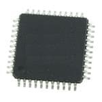
Features • 80C52 Compatible – 8051 Pin and Instruction Compatible – Four 8-bit I/O ports + 2 I/O 2-wire Interface (TWI) Pins – Three 16-bit Timer/Counters – 256 bytes Scratch Pad RAM – 10 Interrupt Sources with 4 Priority Levels – Dual Data Pointer • Variable Length MOVX for Slow RAM/Peripherals • ISP (In-System-Programming) Using Standard V Power Supply cc • Boot ROM Contains Low Level Flash Programming Routines and a Default Serial 8-bit Flash Loader • High-speed Architecture Microcontroller – In Standard Mode: 40 MHz (Vcc 2.7V to 5.5V, both Internal and external code execution) with 2-wire 60 MHz (Vcc 4.5V to 5.5V and Internal Code execution only) – In X2 mode (6 Clocks/machine cycle) Interface 20 MHz (Vcc 2.7V to 5.5V, both Internal and external code execution) 30 MHz (Vcc 4.5V to 5.5V and Internal Code execution only) – 32K Bytes On-chip Flash Program/Data Memory – Byte and Page (128 Bytes) Erase and Write AT89C51IC2 – 100K Write Cycles • On-chip 1024 Bytes Expanded RAM (XRAM) – Software Selectable Size (0, 256, 512, 768, 1024 Bytes) – 256 Bytes Selected at Reset for TS87C51RB2/RC2 Compatibility • Keyboard Interrupt Interface on Port P1 • 400-Kbits/s Multimaster 2-wire Interface • SPI Interface (Master/Slave Mode) • Sub-clock 32 kHz Crystal Oscillator • 8-bit clock Prescaler • Improved X2 Mode With Independant Selection for CPU and Each Peripheral • Programmable Counter Array 5 Channels with: – High Speed Output – Compare/Capture – Pulse Width Modulator – Watchdog Timer Capabilities • Asynchronous Port Reset • Full-duplex Enhanced UART • Dedicated Baud Rate Generator for UART • Low EMI (Inhibit ALE) • Hardware Watchdog Timer (One-time enabled with Reset-Out) • Power Control Modes: – Idle Mode – Power-down Mode – Power-Off Flag • Power Supply: – 2.7 to 3.6 (3V Version) – 2.7 to 5.5V (5V Version) • Temperature Ranges: Commercial (0 to +70°C) and Industrial (-40°C to +85°C) • Packages: PLC44, VQFP44 Rev. 4301D–8051–02/08 1
Description AT89C51IC2 is a high performance Flash version of the 80C51 8-bit microcontrollers. It contains a 32K bytes Flash memory block for program and data. The 32K bytes Flash memory can be programmed either in parallel mode or in serial mode with the ISP capability or with software. The programming voltage is internally generated from the standard V pin. CC The AT89C51IC2 retains all features of the 80C52 with 256 bytes of internal RAM, a 10-source 4-level interrupt controller and three timer/counters. In addition, the AT89C51IC2 has a 32 kHz Subsidiary clock Oscillator, a Programmable Counter Array, an XRAM of 1024 byte, a Hardware Watchdog Timer, a Keyboard Inter- face, a 2-wire interface, an SPI Interface, a more versatile serial channel that facilitates multiprocessor communication (EUART) and a speed improvement mechanism (X2 mode). The fully static design of the AT89C51IC2 allows to reduce system power consumption by bringing the clock frequency down to any value, even DC, without loss of data. The AT89C51IC2 has 2 software-selectable modes of reduced activity and 8-bit clock prescaler for further reduction in power consumption. In the Idle mode the CPU is frozen while the peripherals and the interrupt system are still operating. In the power-down mode the RAM is saved and all other functions are inoperative. The added features of the AT89C51IC2 make it more powerful for applications that need pulse width modulation, high speed I/O and counting capabilities such as alarms, motor control, corded phones, smart card readers. Table 1. Memory Size PLCC44 TOTAL RAM VQFP44 1.4 Flash (bytes) XRAM (bytes) (bytes) I/O T89C51IC2 32k 1024 1280 34 AT89C51IC2 2 4301D–8051–02/08
AT89C51IC2 Block Diagram Figure 1. Block Diagram RxD TxD Vcc Vss ECI PCA T2EX T2 SDA SCL (1) (1) (1) (1) (2)(2) XTAL1 Flash XTAL2 EUA+RT R2A56M 32K x 8 PCA Timer 2 Two-Wire BRG x8 ALE/PROG C51 CORE IB-bus PSEN CPU EA (2) Timer 0 INT Parallel I/O Ports & Ext Bus Watch Key SPI RD Timer 1 Ctrl Dog Board WR Port 0 Port 1Port 2 Port 3 Port 12 (2) (2)(2) (2)(2) (1)(1)(1)(1) Reset T0 T1 INT0 INT1 P1 P3 P4 P0 P2 MISOMOSISCKSS (1): Alternate function of Port 1 (2): Alternate function of Port 3 3 4301D–8051–02/08
SFR Mapping The Special Function Registers (SFRs) of the AT89C51IC2 fall into the following categories: • C51 core registers: ACC, B, DPH, DPL, PSW, SP • I/O port registers: P0, P1, P2, P3, PI2 • Timer registers: T2CON, T2MOD, TCON, TH0, TH1, TH2, TMOD, TL0, TL1, TL2, RCAP2L, RCAP2H • Serial I/O port registers: SADDR, SADEN, SBUF, SCON • PCA (Programmable Counter Array) registers: CCON, CCAPMx, CL, CH, CCAPxH, CCAPxL (x: 0 to 4) • Power and clock control registers: PCON • Hardware Watchdog Timer registers: WDTRST, WDTPRG • Interrupt system registers: IEN0, IPL0, IPH0, IEN1, IPL1, IPH1 • Keyboard Interface registers: KBE, KBF, KBLS • SPI registers: SPCON, SPSTR, SPDAT • 2-wire Interface registers: SSCON, SSCS, SSDAT, SSADR • BRG (Baud Rate Generator) registers: BRL, BDRCON • Flash register: FCON • Clock Prescaler register: CKRL • 32 kHz Sub Clock Oscillator registers: CKSEL, OSSCON AT89C51IC2 4 4301D–8051–02/08
AT89C51IC2 Table 2. C51 Core SFRs Mnemonic Add Name 7 6 5 4 3 2 1 0 ACC E0h Accumulator B F0h B Register PSW D0h Program Status Word CY AC F0 RS1 RS0 OV F1 P SP 81h Stack Pointer DPL 82h Data Pointer Low byte DPH 83h Data Pointer High byte Table 3. System Management SFRs Mnemonic Add Name 7 6 5 4 3 2 1 0 PCON 87h Power Control SMOD1 SMOD0 - - GF1 GF0 PD IDL EXTRA AUXR 8Eh Auxiliary Register 0 - - M0 XRS1 XRS0 AO M ENBOO AUXR1 A2h Auxiliary Register 1 - - - GF3 0 - DPS T CKRL 97h Clock Reload Register - - - - - - - - CKSEL 85h Clock Selection Register - - - - - - - CKS OSCON 86h Oscillator Control Register - - - - - SCLKT0 OscBEn OscAEn CKCKON0 8Fh Clock Control Register 0 TWIX2 WDTX2 PCAX2 SIX2 T2X2 T1X2 T0X2 X2 CKCKON1 AFh Clock Control Register 1 - - - - - - - SPIX2 Table 4. Interrupt SFRs Mnemonic Add Name 7 6 5 4 3 2 1 0 IEN0 A8h Interrupt Enable Control 0 EA EC ET2 ES ET1 EX1 ET0 EX0 IEN1 B1h Interrupt Enable Control 1 - - - - - ESPI ETWI KBD IPH0 B7h Interrupt Priority Control High 0 - PPCH PT2H PHS PT1H PX1H PT0H PX0H IPL0 B8h Interrupt Priority Control Low 0 - PPCL PT2L PLS PT1L PX1L PT0L PX0L IPH1 B3h Interrupt Priority Control High 1 - - - - - SPIH TWIH KBDH IPL1 B2h Interrupt Priority Control Low 1 - - - - - SPIL TWIL KBDL 5 4301D–8051–02/08
Table 5. Port SFRs Mnemonic Add Name 7 6 5 4 3 2 1 0 P0 80h 8-bit Port 0 P1 90h 8-bit Port 1 P2 A0h 8-bit Port 2 P3 B0h 8-bit Port 3 Table 6. Timer SFRs Mnemonic Add Name 7 6 5 4 3 2 1 0 TCON 88h Timer/Counter 0 and 1 Control TF1 TR1 TF0 TR0 IE1 IT1 IE0 IT0 TMOD 89h Timer/Counter 0 and 1 Modes GATE1 C/T1# M11 M01 GATE0 C/T0# M10 M00 TL0 8Ah Timer/Counter 0 Low Byte TH0 8Ch Timer/Counter 0 High Byte TL1 8Bh Timer/Counter 1 Low Byte TH1 8Dh Timer/Counter 1 High Byte WDTRST A6h WatchDog Timer Reset WDTPRG A7h WatchDog Timer Program - - - - - WTO2 WTO1 WTO0 T2CON C8h Timer/Counter 2 control TF2 EXF2 RCLK TCLK EXEN2 TR2 C/T2# CP/RL2# T2MOD C9h Timer/Counter 2 Mode - - - - - - T2OE DCEN Timer/Counter 2 Reload/Capture RCAP2H CBh High byte Timer/Counter 2 Reload/Capture RCAP2L CAh Low byte TH2 CDh Timer/Counter 2 High Byte TL2 CCh Timer/Counter 2 Low Byte Table 7. PCA SFRs Mnemo -nic Add Name 7 6 5 4 3 2 1 0 CCON D8h PCA Timer/Counter Control CF CR - CCF4 CCF3 CCF2 CCF1 CCF0 CMOD D9h PCA Timer/Counter Mode CIDL WDTE - - - CPS1 CPS0 ECF CL E9h PCA Timer/Counter Low byte CH F9h PCA Timer/Counter High byte AT89C51IC2 6 4301D–8051–02/08
AT89C51IC2 Table 7. PCA SFRs (Continued) Mnemo -nic Add Name 7 6 5 4 3 2 1 0 CCAPM0 DAh PCA Timer/Counter Mode 0 ECOM0 CAPP0 CAPN0 MAT0 TOG0 PWM0 ECCF0 CCAPM1 DBh PCA Timer/Counter Mode 1 ECOM1 CAPP1 CAPN1 MAT1 TOG1 PWM1 ECCF1 CCAPM2 DCh PCA Timer/Counter Mode 2 - ECOM2 CAPP2 CAPN2 MAT2 TOG2 PWM2 ECCF2 CCAPM3 DDh PCA Timer/Counter Mode 3 ECOM3 CAPP3 CAPN3 MAT3 TOG3 PWM3 ECCF3 CCAPM4 DEh PCA Timer/Counter Mode 4 ECOM4 CAPP4 CAPN4 MAT4 TOG4 PWM4 ECCF4 CCAP0H FAh PCA Compare Capture Module 0 H CCAP0H7 CCAP0H6 CCAP0H5 CCAP0H4 CCAP0H3 CCAP0H2 CCAP0H1 CCAP0H0 CCAP1H FBh PCA Compare Capture Module 1 H CCAP1H7 CCAP1H6 CCAP1H5 CCAP1H4 CCAP1H3 CCAP1H2 CCAP1H1 CCAP1H0 CCAP2H FCh PCA Compare Capture Module 2 H CCAP2H7 CCAP2H6 CCAP2H5 CCAP2H4 CCAP2H3 CCAP2H2 CCAP2H1 CCAP2H0 CCAP3H FDh PCA Compare Capture Module 3 H CCAP3H7 CCAP3H6 CCAP3H5 CCAP3H4 CCAP3H3 CCAP3H2 CCAP3H1 CCAP3H0 CCAP4H FEh PCA Compare Capture Module 4 H CCAP4H7 CCAP4H6 CCAP4H5 CCAP4H4 CCAP4H3 CCAP4H2 CCAP4H1 CCAP4H0 CCAP0L EAh PCA Compare Capture Module 0 L CCAP0L7 CCAP0L6 CCAP0L5 CCAP0L4 CCAP0L3 CCAP0L2 CCAP0L1 CCAP0L0 CCAP1L EBh PCA Compare Capture Module 1 L CCAP1L7 CCAP1L6 CCAP1L5 CCAP1L4 CCAP1L3 CCAP1L2 CCAP1L1 CCAP1L0 CCAP2L ECh PCA Compare Capture Module 2 L CCAP2L7 CCAP2L6 CCAP2L5 CCAP2L4 CCAP2L3 CCAP2L2 CCAP2L1 CCAP2L0 CCAP3L EDh PCA Compare Capture Module 3 L CCAP3L7 CCAP3L6 CCAP3L5 CCAP3L4 CCAP3L3 CCAP3L2 CCAP3L1 CCAP3L0 CCAP4L EEh PCA Compare Capture Module 4 L CCAP4L7 CCAP4L6 CCAP4L5 CCAP4L4 CCAP4L3 CCAP4L2 CCAP4L1 CCAP4L0 Table 8. Serial I/O Port SFRs Mnemonic Add Name 7 6 5 4 3 2 1 0 SCON 98h Serial Control FE/SM0 SM1 SM2 REN TB8 RB8 TI RI SBUF 99h Serial Data Buffer SADEN B9h Slave Address Mask SADDR A9h Slave Address BDRCON 9Bh Baud Rate Control BRR TBCK RBCK SPD SRC BRL 9Ah Baud Rate Reload Table 9. SPI Controller SFRs Mnemonic Add Name 7 6 5 4 3 2 1 0 SPCON C3h SPI Control SPR2 SPEN SSDIS MSTR CPOL CPHA SPR1 SPR0 SPSTA C4h SPI Status SPIF WCOL SSERR MODF - - - - SPDAT C5h SPI Data SPD7 SPD6 SPD5 SPD4 SPD3 SPD2 SPD1 SPD0 7 4301D–8051–02/08
Table 10. Two-Wire Interface Controller SFRs Mnemonic Add Name 7 6 5 4 3 2 1 0 SSCON 93h Synchronous Serial control SSCR2 SSPE SSSTA SSSTO SSI SSAA SSCR1 SSCR0 SSCS 94h Synchronous Serial Status SSC4 SSC3 SSC2 SSC1 SSC0 0 0 0 SSDAT 95h Synchronous Serial Data SSD7 SSD6 SSD5 SSD4 SSD3 SSD2 SSD1 SSD0 SSADR 96h Synchronous Serial Address SSA7 SSA6 SSA5 SSA4 SSA3 SSA2 SSA1 SSGC Table 11. Keyboard Interface SFRs Mnemonic Add Name 7 6 5 4 3 2 1 0 KBLS 9Ch Keyboard Level Selector KBLS7 KBLS6 KBLS5 KBLS4 KBLS3 KBLS2 KBLS1 KBLS0 KBE 9Dh Keyboard Input Enable KBE7 KBE6 KBE5 KBE4 KBE3 KBE2 KBE1 KBE0 KBF 9Eh Keyboard Flag Register KBF7 KBF6 KBF5 KBF4 KBF3 KBF2 KBF1 KBF0 AT89C51IC2 8 4301D–8051–02/08
AT89C51IC2 Table below shows all SFRs with their address and their reset value. Table 12. SFR Mapping Bit addressable Non Bit addressable 0/8 1/9 2/A 3/B 4/C 5/D 6/E 7/F CH CCAP0H CCAP1H CCAPL2H CCAPL3H CCAPL4H F8h FFh 0000 0000 XXXX XXXX XXXX XXXX XXXX XXXX XXXX XXXX XXXX XXXX B F0h F7h 0000 0000 CL CCAP0L CCAP1L CCAPL2L CCAPL3L CCAPL4L E8h EFh 0000 0000 XXXX XXXX XXXX XXXX XXXX XXXX XXXX XXXX XXXX XXXX ACC E0h E7h 0000 0000 CCON CMOD CCAPM0 CCAPM1 CCAPM2 CCAPM3 CCAPM4 D8h DFh 00X0 0000 00XX X000 X000 0000 X000 0000 X000 0000 X000 0000 X000 0000 PSW FCON (1) D0h D7h 0000 0000 XXXX 0000 T2CON T2MOD RCAP2L RCAP2H TL2 TH2 C8h CFh 0000 0000 XXXX XX00 0000 0000 0000 0000 0000 0000 0000 0000 PI2 bit SPCON SPSTA SPDAT C0h addressable C7h 0001 0100 0000 0000 XXXX XXXX XXXX XX11 IPL0 SADEN B8h BFh X000 000 0000 0000 P3 IEN1 IPL1 IPH1 IPH0 B0h B7h 1111 1111 XXXX X000 XXXX X000 XXXX X111 X000 0000 IEN0 SADDR CKCON1 A8h AFh 0000 0000 0000 0000 XXXX XXX0 P2 AUXR1 WDTRST WDTPRG A0h A7h 1111 1111 XXXX X0X0 XXXX XXXX XXXX X000 SCON SBUF BRL BDRCON KBLS KBE KBF 98h 9Fh 0000 0000 XXXX XXXX 0000 0000 XXX0 0000 0000 0000 0000 0000 0000 0000 P1 SSCON SSCS SSDAT SSADR CKRL 90h 97h 1111 1111 0000 0000 1111 1000 1111 1111 1111 1110 1111 1111 TCON TMOD TL0 TL1 TH0 TH1 AUXR CKCON0 88h 8Fh 0000 0000 0000 0000 0000 0000 0000 0000 0000 0000 0000 0000 XX0X 0000 0000 0000 P0 SP DPL DPH CKSEL OSSCON PCON 80h 87h 1111 1111 0000 0111 0000 0000 0000 0000 XXXX XXX0 XXXX X001 00X1 0000 0/8 1/9 2/A 3/B 4/C 5/D 6/E 7/F reserved 9 4301D–8051–02/08
Pin Configurations Figure 2. Pin Configurations 1 SS ALB CEX1 CEX0 ECI T2EX/ T2/XT B2 AD0 AD1 AD2 AD3 P1.4/ P1.3/ P1.2/ P1.1/ P1.0/ XTAL VCC P0.0/ P0.1/ P0.2/ P0.3/ 6 5 4 3 2 1 4443424140 P1.5/CEX2/MISO 7 39 P0.4/AD4 P1.6/CEX3/SCK 8 38 P0.5/AD5 P1.7/CEx4/MOSI 9 37 P0.6/AD6 RST 10 36 P0.7/AD7 P3.0/RxD 11 35 EA PI2.1/SDA 12 PLCC44 34 PI2.0/SCL P3.1/TxD 13 33 ALE/PROG P3.2/INT0 14 32 PSEN P3.3/INT1 15 31 P2.7/A15 P3.4/T0 16 30 P2.6/A14 P3.5/T1 17 29 P2.5/A13 1819202122232425262728 P3.6/WR P3.7/RD XTAL2 XTAL1 VSS NIC* P2.0/A8 P2.1/A9 P2.2/A10 P2.3/A11 P2.4/A12 1 B S L S A CEX1 CEX0 ECI T2EX/ T2/XT B2 AD0 AD1 AD2 AD3 1.4/ 1.3/ 1.2/ 1.1/ 1.0/ TAL CC 0.0/ 0.1/ 0.2/ 0.3/ P P P P P X V P P P P 444 34 24 14 03 93837363534 P1.5/CEX2/MISO 1 33 P0.4/AD4 P1.6/CEX3/SCK 2 32 P0.5/AD5 P1.7/CEX4/MOSI 3 31 P0.6/AD6 RST 4 30 P0.7/AD7 P3.0/RxD 5 29 EA PI2.1/SDA 6 VQFP44 1.4 28 PI2.0/SCL P3.1/TxD 7 27 ALE/PROG P3.2/INT0 8 26 PSEN P3.3/INT1 9 25 P2.7/A15 P3.4/T0 10 24 P2.6/A14 P3.5/T1 11 23 P2.5/A13 1213141516171819202122 P3.6/WR P3.7/RD XTAL2 XTAL1 VSS NIC* P2.0/A8 P2.1/A9 P2.2/A10 P2.3/A11 P2.4/A12 AT89C51IC2 10 4301D–8051–02/08
AT89C51IC2 Table 13. Pin Description for 40/44 Pin Packages Pin Number Type Mnemonic PLCC44 VQFP44 1.4 Name and Function V 22 16 I Ground: 0V reference SS Power Supply: This is the power supply voltage for normal, idle and power-down V 44 38 I CC operation P0.0 - P0.7 43 - 36 37 - 30 I/O Port 0: Port 0 is an open-drain, bidirectional I/O port. Port 0 pins that have 1s written to them float and can be used as high impedance inputs. Port 0 must be polarized to V CC or V in order to prevent any parasitic current consumption. Port 0 is also the multi- SS plexed low-order address and data bus during access to external program and data memory. In this application, it uses strong internal pull-up when emitting 1s. Port 0 also inputs the code bytes during EPROM programming. External pull-ups are required dur- ing program verification during which P0 outputs the code bytes. P1.0 - P1.7 2 - 9 40 - 44 I/O Port 1: Port 1 is an 8-bit bidirectional I/O port with internal pull-ups. Port 1 pins that 1 - 3 have 1s written to them are pulled high by the internal pull-ups and can be used as inputs. As inputs, Port 1 pins that are externally pulled low will source current because of the internal pull-ups. Port 1 also receives the low-order address byte during memory programming and verification. Alternate functions for AT89C51IC2 Port 1 include: 2 40 I/O P1.0: Input/Output I/O T2 (P1.0): Timer/Counter 2 external count input/Clockout I XTALB1 (P1.0): Sub Clock input to the inverting oscillator amplifier 3 41 I/O P1.1: Input/Output I T2EX: Timer/Counter 2 Reload/Capture/Direction Control I SS: SPI Slave Select 4 42 I/O P1.2: Input/Output I ECI: External Clock for the PCA 5 43 I/O P1.3: Input/Output I/O CEX0: Capture/Compare External I/O for PCA module 0 6 44 I/O P1.4: Input/Output I/O CEX1: Capture/Compare External I/O for PCA module 1 7 1 I/O P1.5: Input/Output I/O CEX2: Capture/Compare External I/O for PCA module 2 I/O MISO: SPI Master Input Slave Output line When SPI is in master mode, MISO receives data from the slave peripheral. When SPI is in slave mode, MISO outputs data to the master controller. 8 2 I/O P1.6: Input/Output I/O CEX3: Capture/Compare External I/O for PCA module 3 I/O SCK: SPI Serial Clock SCK outputs clock to the slave peripheral 11 4301D–8051–02/08
Table 13. Pin Description for 40/44 Pin Packages (Continued) Pin Number Type Mnemonic PLCC44 VQFP44 1.4 Name and Function 9 3 I/O P1.7: Input/Output: I/O CEX4: Capture/Compare External I/O for PCA module 4 I/O MOSI: SPI Master Output Slave Input line When SPI is in master mode, MOSI outputs data to the slave peripheral. When SPI is in slave mode, MOSI receives data from the master controller. Crystal A 1: Input to the inverting oscillator amplifier and input to the internal clock XTALA1 21 15 I generator circuits. XTALA2 20 14 O Crystal A 2: Output from the inverting oscillator amplifier XTALB1 2 40 I Crystal B 1: (Sub Clock) Input to the inverting oscillator amplifier and input to the inter- nal clock generator circuits. XTALB2 1 39 O Crystal B 2: (Sub Clock) Output from the inverting oscillator amplifier P2.0 - P2.7 24 - 31 18 - 25 I/O Port 2: Port 2 is an 8-bit bidirectional I/O port with internal pull-ups. Port 2 pins that have 1s written to them are pulled high by the internal pull-ups and can be used as inputs. As inputs, Port 2 pins that are externally pulled low will source current because of the internal pull-ups. Port 2 emits the high-order address byte during fetches from external program memory and during accesses to external data memory that use 16-bit addresses (MOVX @DPTR).In this application, it uses strong internal pull-ups emitting 1s. During accesses to external data memory that use 8-bit addresses (MOVX @Ri), port 2 emits the contents of the P2 SFR. Some Port 2 pins receive the high order address bits during EPROM programming and verification. P3.0 - P3.7 11, 5, I/O Port 3: Port 3 is an 8-bit bidirectional I/O port with internal pull-ups. Port 3 pins that 13 - 19 7 - 13 have 1s written to them are pulled high by the internal pull-ups and can be used as inputs. As inputs, Port 3 pins that are externally pulled low will source current because of the internal pull-ups. Port 3 also serves the special features of the 80C51 family, as listed below. 11 5 I RXD (P3.0): Serial input port 13 7 O TXD (P3.1): Serial output port 14 8 I INT0 (P3.2): External interrupt 0 15 9 I INT1 (P3.3): External interrupt 1 16 10 I T0 (P3.4): Timer 0 external input 17 11 I T1 (P3.5): Timer 1 external input 18 12 O WR (P3.6): External data memory write strobe 19 13 O RD (P3.7): External data memory read strobe PI2.0 - PI2.1 Port I2: Port I2 is an open drain. It can be used as inputs (must be polarized to Vcc 34, 12 28, 6 with external resistor to prevent any parasitic current consumption). 34 28 I/O SCL (PI2.0): 2-wire Serial Clock SCL output the serial clock to slave peripherals SCL input the serial clock from master 12 6 I/O SDA (PI2.1): 2-wire Serial Data AT89C51IC2 12 4301D–8051–02/08
AT89C51IC2 Table 13. Pin Description for 40/44 Pin Packages (Continued) Pin Number Type Mnemonic PLCC44 VQFP44 1.4 Name and Function SDA is the bidirectional 2-wire data line Reset: A high on this pin for two machine cycles while the oscillator is running, resets the device. An internal diffused resistor to V permits a power-on reset using only an RST 10 4 I/O SS external capacitor to V . This pin is an output when the hardware watchdog forces a CC system reset. ALE/PROG 33 27 O (I) Address Latch Enable/Program Pulse: Output pulse for latching the low byte of the address during an access to external memory. In normal operation, ALE is emitted at a constant rate of 1/6 (1/3 in X2 mode) the oscillator frequency, and can be used for external timing or clocking. Note that one ALE pulse is skipped during each access to external data memory. This pin is also the program pulse input (PROG) during Flash programming. ALE can be disabled by setting SFR’s AUXR.0 bit. With this bit set, ALE will be inactive during internal fetches. PSEN 32 26 O Program Strobe ENable: The read strobe to external program memory. When execut- ing code from the external program memory, PSEN is activated twice each machine cycle, except that two PSEN activations are skipped during each access to external data memory. PSEN is not activated during fetches from internal program memory. EA 35 29 I External Access Enable: EA must be externally held low to enable the device to fetch code from external program memory locations 0000H to FFFFH (RD). If security level 1 is programmed, EA will be internally latched on Reset. 13 4301D–8051–02/08
Oscillators Overview Two oscillators are available for CPU: • OSCA used for high frequency: Up to 48 MHz @5V +/- 10% • OSCB used for low frequency: 32.768 kHz Several operating modes are available and programmable by software: • to switch OSCA to OSCB and vice-versa • to stop OSCA or OSCB to reduce consumption In order to optimize the power consumption and the execution time needed for a specific task, an internal prescaler feature has been implemented between the selected oscilla- tor and the CPU. Registers Table 14. CKSEL Register CKSEL - Clock Selection Register (85h) 7 6 5 4 3 2 1 0 - - - - - - - CKS Bit Bit Number Mnemonic Description 7 - Reserved 6 - Reserved 5 - Reserved 4 - Reserved 3 - Reserved 2 - Reserved 1 - Reserved CPU Oscillator Select Bit: (CKS) Cleared, CPU and peripherals connected to OSCB 0 CKS Set, CPU and peripherals connected to OSCA Programmed by hardware after a Power-up regarding Hardware Security Byte (HSB).HSB.OSC (Default setting, OSCA selected) Reset Value = 0000 000’HSB.OSC’b (see Hardware Security Byte (HSB) Table84) Not bit addressable AT89C51IC2 14 4301D–8051–02/08
AT89C51IC2 Table 15. OSCCON Register OSCCON- Oscillator Control Register (86h) 7 6 5 4 3 2 1 0 - - - - - SCLKT0 OscBEn OscAEn Bit Bit Number Mnemonic Description 7 - Reserved 6 - Reserved 5 - Reserved 4 - Reserved 3 - Reserved Sub Clock Timer0 Cleared by software to select T0 pin 2 SCLKT0 Set by software to select T0 Sub Clock Cleared by hardware after a Power Up OscB enable bit Set by software to run OscB 1 OscBEn Cleared by software to stop OscB Programmed by hardware after a Power-up regarding HSB.OSC (Default cleared, OSCB stopped) OscA enable bit Set by software to run OscA 0 OscAEn Cleared by software to stop OscA Programmed by hardware after a Power-up regarding HSB.OSC(Default Set, OSCA runs) Reset Value = XXXX X0’HSB.OSC’’HSB.OSC’b (see Hardware Security Byte (HSB) Table84) Not bit addressable Table 16. CKRL Register CKRL - Clock Reload Register 7 6 5 4 3 2 1 0 - - - - - - - - Bit Number Mnemonic Description Clock Reload Register: 7:0 CKRL Prescaler value Reset Value = 1111 1111b Not bit addressable 15 4301D–8051–02/08
Table 17. PCON Register PCON - Power Control Register (87h) 7 6 5 4 3 2 1 0 SMOD1 SMOD0 - POF GF1 GF0 PD IDL Bit Bit Number Mnemonic Description Serial port Mode bit 1 7 SMOD1 Set to select double baud rate in mode 1, 2 or 3. Serial port Mode bit 0 6 SMOD0 Cleared to select SM0 bit in SCON register. Set to select FE bit in SCON register. Reserved 5 - The value read from this bit is indeterminate. Do not set this bit. Power-Off Flag Cleared to recognize next reset type. 4 POF Set by hardware when VCC rises from 0 to its nominal voltage. Can also be set by software. General purpose Flag 3 GF1 Cleared by software for general purpose usage. Set by software for general purpose usage. General purpose Flag 2 GF0 Cleared by software for general purpose usage. Set by software for general purpose usage. Power-Down mode bit 1 PD Cleared by hardware when reset occurs. Set to enter power-down mode. Idle mode bit 0 IDL Cleared by hardware when interrupt or reset occurs. Set to enter idle mode. Reset Value = 00X1 0000b Not bit addressable AT89C51IC2 16 4301D–8051–02/08
AT89C51IC2 Functional Block Diagram Figure 3. Functional Oscillator Block Diagram Reload Reset PwdOscA CKRL FOSCA XtalA1 OscA 1 XtalA2 8-bit :2 0 Prescaler-Divider 1 OscAEn 1 OSCCON X2 0 CLK Peripheral Clock CKCON0 PERIPH 0 CLK CPU clock CKRL=0xFF? CPU Idle CKS FOSCB CKSEL PwdOscB XtalB1 OscB :128 Sub XtalB2 Clock OscBEn OSCCON Operating Modes Reset A hardware RESET puts the Clock generator in the following state: The selected oscillator depends on OSC bit in Hardware Security Byte (HSB) (see HSB Table 84) HSB.OSC = 1 (Oscillator A selected) • OscAEn = 1 & OscBEn = 0: OscA is running, OscB is stopped. • CKS = 1: OscA is selected for CPU. HSB.OSC = 0 (Oscillator B selected) • OscAEn = 0 & OscBEn = 1: OscB is running, OscA is stopped. • CKS = 0: OscB is selected for CPU. Functional Modes Normal Modes • CPU and Peripherals clock depend on the software selection using CKCON0, CKCON1 and CKRL registers • CKS bit in CKSEL register selects either OscA or OscB • CKRL register determines the frequency of the OscA clock. 17 4301D–8051–02/08
• It is always possible to switch dynamically by software from OscA to OscB, and vice versa by changing CKS bit. Idle Modes • IDLE modes are achieved by using any instruction that writes into PCON.0 bit (IDL) • IDLE modes A and B depend on previous software sequence, prior to writing into PCON.0 bit: • IDLE MODE A: OscA is running (OscAEn = 1) and selected (CKS = 1) • IDLE MODE B: OscB is running (OscBEn = 1) and selected (CKS = 0) • The unused oscillator OscA or OscB can be stopped by software by clearing OscAEn or OscBEn respectively. • IDLE mode can be canceled either by Reset, or by activation of any enabled interruption • In both cases, PCON.0 bit (IDL) is cleared by hardware • Exit from IDLE modes will leave Oscillators control bits (OscEnA, OscEnB, CKS) unchanged. Power Down Modes • POWER DOWN modes are achieved by using any instruction that writes into PCON.1 bit (PD) • POWER DOWN modes A and B depend on previous software sequence, prior to writing into PCON.1 bit: • Both OscA and OscB will be stopped. • POWER DOWN mode can be cancelled either by a hardware Reset, an external interruption, or the keyboard interrupt. • By Reset signal: The CPU will restart according to OSC bit in Hardware Security Bit (HSB) register. • By INT0 or INT1 interruption, if enabled: (standard behavioral), request on Pads must be driven low enough to ensure correct restart of the oscillator which was selected when entering in Power down. • By keyboard Interrupt if enabled: a hardware clear of the PCON.1 flag ensure the restart of the oscillator which was selected when entering in Power down. Table 18. Overview PCON.1 PCON.0 OscBEn OscAEn CKS Selected Mode Comment NORMAL MODE Default mode after power-up or 0 0 0 1 1 A, OscB stopped Warm Reset NORMAL MODE Default mode after power-up or 0 0 1 1 1 A, OscB running Warm Reset + OscB running NORMAL MODE 0 0 1 0 0 OscB running and selected B, OscA stopped NORMAL MODE OscB running and selected + 0 0 1 1 0 B, OscA running OscA running OscA & OscB cannot be stopped X X 0 0 X INVALID at the same time OscA must not be stopped, as X X X 0 1 INVALID used for CPU and peripherals OscB must not be stopped as X X 0 X 0 INVALID used for CPU and peripherals AT89C51IC2 18 4301D–8051–02/08
AT89C51IC2 Table 18. Overview (Continued) PCON.1 PCON.0 OscBEn OscAEn CKS Selected Mode Comment The CPU is off, OscA supplies the 0 1 X 1 1 IDLE MODE A peripherals, OscB can be disabled (OscBEn = 0) The CPU is off, OscB supplies the 0 1 1 X 0 IDLE MODE B peripherals, OscA can be disabled (OscAEn = 0) POWER DOWN The CPU and peripherals are off, 1 X X 1 X MODE OscA and OscB are stopped Design Considerations Oscillators Control • PwdOscA and PwdOscB signals are generated in the Clock generator and used to control the hard blocks of oscillators A and B. • PwdOscA =’1’ stops OscA • PwdOscB =’1’ stops OscB • The following tables summarize the Operating modes: PCON.1 OscAEn PwdOscA Comments 0 1 0 OscA running OscA stopped by 1 X 1 Power-down mode OscA stopped by 0 0 1 clearing OscAEn PCON.1 OscBEn PwdOscB Comments 0 1 0 OscB running OscB stopped by 1 X 1 Power-down mode OscB stopped by 0 0 1 clearing OscBEn Prescaler Divider • A hardware RESET puts the prescaler divider in the following state: – CKRL = FFh: F = F = F /2 (Standard C51 feature) CLK CPU CLK PERIPH OSCA • CKS signal selects OSCA or OSCB: F = F or F CLK OUT OSCA OSCB • Any value between FFh down to 00h can be written by software into CKRL register in order to divide frequency of the selected oscillator: – CKRL = 00h: minimum frequency F = F = F /1020 (Standard Mode) CLK CPU CLK PERIPH OSCA F = F = F /510 (X2 Mode) CLK CPU CLK PERIPH OSCA – CKRL = FFh: maximum frequency F = F = F /2 (Standard Mode) CLK CPU CLK PERIPH OSCA F = F = F (X2 Mode) CLK CPU CLK PERIPH OSCA 19 4301D–8051–02/08
– F and F , for CKRL<>0xFF CLK CPU CLK PERIPH In X2 Mode: F F =F = --------------------O---S---C----A---------------- CPU CLKPERIPH 2×(255–CKRL) In X1 Mode: F F =F = --------------------O---S---C----A---------------- CPU CLKPERIPH 4×(255–CKRL) Timer 0: Clock Inputs Figure 4. Timer 0: Clock Inputs FCLK PERIPH :6 0 Timer 0 1 T0 pin 0 Control Sub Clock 1 C/T TMOD SCLKT0 OSCCON Gate INT0 TR0 Note: The SCLKT0 bit in OSCCON register allows to select Timer 0 Subsidiary clock. SCLKT0 = 0: Timer 0 uses the standard T0 pin as clock input (Standard mode) SCLKT0 = 1: Timer 0 uses the special Sub Clock as clock input, this feature can be use as periodic interrupt for time clock. AT89C51IC2 20 4301D–8051–02/08
AT89C51IC2 Enhanced Features In comparison to the original 80C52, the AT89C51IC2 implements some new features, which are: • The X2 option • The Dual Data Pointer • The extended RAM • The Programmable Counter Array (PCA) • The Hardware Watchdog • The SPI interface • The 2-wire interface • The 4 level interrupt priority system • The power-off flag • The Power On Reset • The ONCE mode • The ALE disabling • Some enhanced features are also located in the UART and the timer 2 X2 Feature and OSCA The AT89C51IC2 core needs only 6 clock periods per machine cycle. This feature Clock Generation called ”X2” provides the following advantages: • Divide frequency crystals by 2 (cheaper crystals) while keeping same CPU power. • Save power consumption while keeping same CPU power (oscillator power saving). • Save power consumption by dividing dynamically the operating frequency by 2 in operating and idle modes. • Increase CPU power by 2 while keeping same crystal frequency. In order to keep the original C51 compatibility, a divider by 2 is inserted between the XTALA1 signal and the main clock input of the core (phase generator). This divider may be disabled by software. Description The clock for the whole circuit and peripherals is first divided by two before being used by the CPU core and the peripherals. This allows any cyclic ratio to be accepted on XTALA1 input. In X2 mode, as this divider is bypassed, the signals on XTALA1 must have a cyclic ratio between 40 to 60%. Figure 5. shows the clock generation block diagram.x2 bit is validated on the rising edge of the XTALA1÷2 to avoid glitches when switching from X2 to STD mode. Figure 6. shows the switching mode waveforms. Figure 5. Clock Generation Diagram CKRL XTALA1:2 FOSCA XTALA1 2 0 8 bit Prescaler 0 FCLK CPU FXTAL 1 1 FCLK PERIPH F OSCB X2 CKS CKCON0 CKSEL 21 4301D–8051–02/08
Figure 6. Mode Switching Waveforms XTALA1 XTALA1:2 X2 bit F CPU clock OSCA STD Mode X2 Mode STD Mode The X2 bit in the CKCON0 register (see Table19) allow to switch from 12 clock periods per instruction to 6 clock periods and vice versa. At reset, the speed is setting according to X2 bit of Hardware Security Byte (HSB). By default, Standard mode is actived. Setting the X2 bit activates the X2 feature (X2 mode). The T0X2, T1X2, T2X2, UartX2, PcaX2, WdX2 and I2CX2 bits in the CKCON0 register (See Table 19.) and SPIX2 bit in the CKCON1 register (see Table20) allow to switch from standard peripheral speed (12 clock periods per peripheral clock cycle) to fast peripheral speed (6 clock periods per peripheral clock cycle). These bits are active only in X2 mode. More information about the X2 mode can be found in the application note "How to take advantage of the X2 features in TS80C51 microcontroller?" AT89C51IC2 22 4301D–8051–02/08
AT89C51IC2 Table 19. CKCON0 Register CKCON0 - Clock Control Register (8Fh) 7 6 5 4 3 2 1 0 SPIX2 WDX2 PCAX2 SIX2 T2X2 T1X2 T0X2 X2 Bit Bit Number Mnemonic Description 2-wire clock (This control bit is validated when the CPU clock X2 is set; when X2 is low, this bit has no effect) 7 I2CX2 Cleared to select 6 clock periods per peripheral clock cycle. Set to select 12 clock periods per peripheral clock cycle. Watchdog clock (This control bit is validated when the CPU clock X2 is set; when X2 is low, this bit has no effect) 6 WDX2 Cleared to select 6 clock periods per peripheral clock cycle. Set to select 12 clock periods per peripheral clock cycle. Programmable Counter Array clock (This control bit is validated when the CPU clock X2 is set; when X2 is low, this bit has no effect) 5 PCAX2 Cleared to select 6 clock periods per peripheral clock cycle. Set to select 12 clock periods per peripheral clock cycle. Enhanced UART clock (Mode 0 and 2) (This control bit is validated when the CPU clock X2 is set; when X2 is low, this bit has no effect) 4 SIX2 Cleared to select 6 clock periods per peripheral clock cycle. Set to select 12 clock periods per peripheral clock cycle. Timer2 clock (This control bit is validated when the CPU clock X2 is set; when X2 is low, this bit has no effect) 3 T2X2 Cleared to select 6 clock periods per peripheral clock cycle. Set to select 12 clock periods per peripheral clock cycle. Timer1 clock (This control bit is validated when the CPU clock X2 is set; when X2 is low, this bit has no effect) 2 T1X2 Cleared to select 6 clock periods per peripheral clock cycle. Set to select 12 clock periods per peripheral clock cycle. Timer0 clock (This control bit is validated when the CPU clock X2 is set; when X2 is low, this bit has no effect) 1 T0X2 Cleared to select 6 clock periods per peripheral clock cycle. Set to select 12 clock periods per peripheral clock cycle. CPU clock Cleared to select 12 clock periods per machine cycle (STD mode) for CPU and all the peripherals. 0 X2 Set to select 6clock periods per machine cycle (X2 mode) and to enable the individual peripherals "X2" bits. Programmed by hardware after Power-up regarding Hardware Security Byte (HSB), Default setting, X2 is cleared. Reset Value = 0000 000’HSB.X2’b Not bit addressable 23 4301D–8051–02/08
Table 20. CKCON1 Register CKCON1 - Clock Control Register (AFh) 7 6 5 4 3 2 1 0 - - - - - - - SPIX2 Bit Bit Number Mnemonic Description 7 - Reserved 6 - Reserved 5 - Reserved 4 - Reserved 3 - Reserved 2 - Reserved 1 - Reserved SPI (This control bit is validated when the CPU clock X2 is set; when X2 is low, this bit has no effect) 0 SPIX2 Clear to select 6 clock periods per peripheral clock cycle. Set to select 12 clock periods per peripheral clock cycle. Reset Value = XXXX XXX0b Not bit addressable AT89C51IC2 24 4301D–8051–02/08
AT89C51IC2 Dual Data Pointer The additional data pointer can be used to speed up code execution and reduce code Register size. The dual DPTR structure is a way by which the chip will specify the address of an exter- nal data memory location. There are two 16-bit DPTR registers that address the external memory, and a single bit called DPS = AUXR1.0 (see Table21) that allows the program code to switch between them (Refer to Figure7). Figure 7. Use of Dual Pointer External Data Memory 7 0 DPS DPTR1 AUXR1(A2H) DPTR0 DPH(83H) DPL(82H) Table 21. AUXR1 register AUXR1- Auxiliary Register 1(0A2h) 7 6 5 4 3 2 1 0 - - ENBOOT - GF3 0 - DPS Bit Bit Number Mnemonic Description Reserved 7 - The value read from this bit is indeterminate. Do not set this bit. Reserved 6 - The value read from this bit is indeterminate. Do not set this bit. Enable Boot Flash 5 ENBOOT Cleared to disable boot rom. Set to map the boot rom between F800h - 0FFFFh. Reserved 4 - The value read from this bit is indeterminate. Do not set this bit. 3 GF3 This bit is a general purpose user flag.* 2 0 Always cleared. Reserved 1 - The value read from this bit is indeterminate. Do not set this bit. Data Pointer Selection 0 DPS Cleared to select DPTR0. Set to select DPTR1. Reset Value: XXXX XX0X0b Not bit addressable Note: *Bit 2 stuck at 0; this allows to use INC AUXR1 to toggle DPS without changing GF3. 25 4301D–8051–02/08
ASSEMBLY LANGUAGE ; Block move using dual data pointers ; Modifies DPTR0, DPTR1, A and PSW ; note: DPS exits opposite of entry state ; unless an extra INC AUXR1 is added ; 00A2 AUXR1 EQU 0A2H ; 0000 909000MOV DPTR,#SOURCE ; address of SOURCE 0003 05A2 INC AUXR1 ; switch data pointers 0005 90A000 MOV DPTR,#DEST ; address of DEST 0008 LOOP: 0008 05A2 INC AUXR1 ; switch data pointers 000A E0 MOVX A,@DPTR ; get a byte from SOURCE 000B A3 INC DPTR ; increment SOURCE address 000C 05A2 INC AUXR1 ; switch data pointers 000E F0 MOVX @DPTR,A ; write the byte to DEST 000F A3 INC DPTR ; increment DEST address 0010 70F6JNZ LOOP ; check for 0 terminator 0012 05A2 INC AUXR1 ; (optional) restore DPS INC is a short (2 bytes) and fast (12 clocks) way to manipulate the DPS bit in the AUXR1 SFR. However, note that the INC instruction does not directly force the DPS bit to a par- ticular state, but simply toggles it. In simple routines, such as the block move example, only the fact that DPS is toggled in the proper sequence matters, not its actual value. In other words, the block move routine works the same whether DPS is '0' or '1' on entry. Observe that without the last instruction (INC AUXR1), the routine will exit with DPS in the opposite state. AT89C51IC2 26 4301D–8051–02/08
AT89C51IC2 Expanded RAM The AT89C51IC2 provides additional Bytes of random access memory (RAM) space for (XRAM) increased data parameter handling and high level language usage. AT89C51IC2 devices have expanded RAM in external data space; maximum size and location are described in Table 22. Table 22. Expanded RAM Address XRAM size Start End AT89C51IC2 1024 00h 3FFh The AT89C51IC2 has internal data memory that is mapped into four separate segments. The four segments are: 1. The Lower 128 bytes of RAM (addresses 00h to 7Fh) are directly and indirectly addressable. 2. The Upper 128 bytes of RAM (addresses 80h to FFh) are indirectly addressable only. 3. The Special Function Registers, SFRs, (addresses 80h to FFh) are directly address- able only. 4. The expanded RAM bytes are indirectly accessed by MOVX instructions, and with the EXTRAM bit cleared in the AUXR register (see Table22) The lower 128 bytes can be accessed by either direct or indirect addressing. The Upper 128 bytes can be accessed by indirect addressing only. The Upper 128 bytes occupy the same address space as the SFR. That means they have the same address, but are physically separate from SFR space. Figure 8. Internal and External Data Memory Address 0FFh or 3FFh 0FFh 0FFh 0FFFFh Upper 128 bytes Special External Internal Function Data Ram Register Memory direct accesses indirect accesses XRAM 80h 80h 7Fh Lower 128 bytes Internal Ram direct or indirect accesses 00FFh up to 03FFh 00 00 0000 When an instruction accesses an internal location above address 7Fh, the CPU knows whether the access is to the upper 128 bytes of data RAM or to SFR space by the addressing mode used in the instruction. • Instructions that use direct addressing access SFR space. For example: MOV 0A0H, # data, accesses the SFR at location 0A0h (which is P2). 27 4301D–8051–02/08
• Instructions that use indirect addressing access the Upper 128 bytes of data RAM. For example: MOV @R0, # data where R0 contains 0A0h, accesses the data byte at address 0A0h, rather than P2 (whose address is 0A0h). • The XRAM bytes can be accessed by indirect addressing, with EXTRAM bit cleared and MOVX instructions. This part of memory which is physically located on-chip, logically occupies the first bytes of external data memory. The bits XRS0 and XRS1 are used to hide a part of the available XRAM as explained in Table22. This can be useful if external peripherals are mapped at addresses already used by the internal XRAM. • With EXTRAM = 0, the XRAM is indirectly addressed, using the MOVX instruction in combination with any of the registers R0, R1 of the selected bank or DPTR. An access to XRAM will not affect ports P0, P2, P3.6 (WR) and P3.7 (RD). For example, with EXTRAM = 0, MOVX @R0, # data where R0 contains 0A0H, accesses the XRAM at address 0A0H rather than external memory. An access to external data memory locations higher than the accessible size of the XRAM will be performed with the MOVX DPTR instructions in the same way as in the standard 80C51, with P0 and P2 as data/address busses, and P3.6 and P3.7 as write and read timing signals. Accesses to XRAM above 0FFH can only be done by the use of DPTR. • With EXTRAM = 1, MOVX @Ri and MOVX @DPTR will be similar to the standard 80C51. MOVX @ Ri will provide an eight-bit address multiplexed with data on Port0 and any output port pins can be used to output higher order address bits. This is to provide the external paging capability. MOVX @DPTR will generate a sixteen-bit address. Port2 outputs the high-order eight address bits (the contents of DPH) while Port0 multiplexes the low-order eight address bits (DPL) with data. MOVX @ Ri and MOVX @DPTR will generate either read or write signals on P3.6 (WR) and P3.7 (RD). The stack pointer (SP) may be located anywhere in the 256 bytes RAM (lower and upper RAM) internal data memory. The stack may not be located in the XRAM. The M0 bit allows to stretch the XRAM timings; if M0 is set, the read and write pulses are extended from 6 to 30 clock periods. This is useful to access external slow peripherals. AT89C51IC2 28 4301D–8051–02/08
AT89C51IC2 Table 23. AUXR Register AUXR - Auxiliary Register (8Eh) 7 6 5 4 3 2 1 0 - - M0 - XRS1 XRS0 EXTRAM AO Bit Bit Number Mnemonic Description Reserved 7 - The value read from this bit is indeterminate. Do not set this bit Reserved 6 - The value read from this bit is indeterminate. Do not set this bit Pulse length Cleared to stretch MOVX control: the RD/ and the WR/ pulse length is 6 clock 5 M0 periods (default). Set to stretch MOVX control: the RD/ and the WR/ pulse length is 30 clock periods. Reserved 4 - The value read from this bit is indeterminate. Do not set this bit 3 XRS1 XRAM Size XRS1 XRS0 XRAM size 0 0 256 bytes (default) 0 1 512 bytes 2 XRS0 1 0 768 bytes 1 1 1024 bytes EXTRAM bit Cleared to access internal XRAM using movx @ Ri/ @ DPTR. 1 EXTRAM Set to access external memory. Programmed by hardware after Power-up regarding Hardware Security Byte (HSB), default setting, XRAM selected. ALE Output bit Cleared, ALE is emitted at a constant rate of 1/6 the oscillator frequency (or 1/3 if 0 AO X2 mode is used) (default) Set, ALE is active only during a MOVX or MOVC instruction is used. Reset Value = XX0X 00’HSB.XRAM’0b Not bit addressable 29 4301D–8051–02/08
Timer 2 The Timer 2 in the AT89C51IC2 is the standard C52 the Timer 2. It is a 16-bit timer/counter: the count is maintained by two eight-bit timer registers, TH2 and TL2 are cascaded. It is controlled by T2CON (Table24) and T2MOD (Table25) registers. Timer 2 operation is similar to Timer 0 and Timer 1. C/T2 selects F /12 OSC (timer operation) or external pin T2 (counter operation) as the timer clock input. Setting TR2 allows TL2 to be incremented by the selected input. Timer 2 has 3 operating modes: capture, autoreload and Baud Rate Generator. These modes are selected by the combination of RCLK, TCLK and CP/RL2 (T2CON). Refer to the Atmel 8-bit Microcontroller Hardware description for the description of Cap- ture and Baud Rate Generator Modes. Timer 2 includes the following enhancements: • Auto-reload mode with up or down counter • Programmable clock-output Auto-Reload Mode The auto-reload mode configures timer 2 as a 16-bit timer or event counter with auto- matic reload. If DCEN bit in T2MOD is cleared, timer 2 behaves as in 80C52 (refer to the Atmel 8-bit Microcontroller Hardware description). If DCEN bit is set, timer 2 acts as an Up/down timer/counter as shown in Figure9. In this mode the T2EX pin controls the direction of count. When T2EX is high, timer 2 counts up. Timer overflow occurs at FFFFh which sets the TF2 flag and generates an interrupt request. The overflow also causes the 16-bit value in RCAP2H and RCAP2L registers to be loaded into the timer registers TH2 and TL2. When T2EX is low, timer 2 counts down. Timer underflow occurs when the count in the timer registers TH2 and TL2 equals the value stored in RCAP2H and RCAP2L registers. The underflow sets TF2 flag and reloads FFFFh into the timer registers. The EXF2 bit toggles when timer 2 overflows or underflows according to the direction of the count. EXF2 does not generate any interrupt. This bit can be used to provide 17-bit resolution. AT89C51IC2 30 4301D–8051–02/08
AT89C51IC2 Figure 9. Auto-Reload Mode Up/Down Counter (DCEN = 1) FCLK PERIPH :6 0 1 T2 C/T2 TR2 T2CON T2CON T2EX: (DOWN COUNTING RELOAD VALUE) if DCEN=1, 1=UP FFh FFh (8-bit) (8-bit) if DCEN=1, 0=DOWN if DCEN = 0, up counting TOGGLE T2CON EXF2 TL2 TH2 TIMER 2 TF2 (8-bit) (8-bit) INTERRUPT T2CON RCAP2L RCAP2H (8-bit) (8-bit) (UP COUNTING RELOAD VALUE) Programmable Clock- In the clock-out mode, timer 2 operates as a 50%-duty-cycle, programmable clock gen- Output erator (See Figure10). The input clock increments TL2 at frequency F /2. The CLK PERIPH timer repeatedly counts to overflow from a loaded value. At overflow, the contents of RCAP2H and RCAP2L registers are loaded into TH2 and TL2. In this mode, timer 2 overflows do not generate interrupts. The formula gives the clock-out frequency as a function of the system oscillator frequency and the value in the RCAP2H and RCAP2L registers: F Clock–OutFrequency = ----------------------------------C---L---K---P---E---R---I--P---H-------------------------------- 4×(65536–RCAP2H⁄RCAP2L) For a 16 MHz system clock, timer 2 has a programmable frequency range of 61 Hz (F /216) to 4 MHz (F /4). The generated clock signal is brought out to CLK PERIPH CLK PERIPH T2 pin (P1.0). Timer 2 is programmed for the clock-out mode as follows: • Set T2OE bit in T2MOD register. • Clear C/T2 bit in T2CON register. • Determine the 16-bit reload value from the formula and enter it in RCAP2H/RCAP2L registers. • Enter a 16-bit initial value in timer registers TH2/TL2. It can be the same as the reload value or a different one depending on the application. • To start the timer, set TR2 run control bit in T2CON register. It is possible to use timer 2 as a baud rate generator and a clock generator simulta- neously. For this configuration, the baud rates and clock frequencies are not independent since both functions use the values in the RCAP2H and RCAP2L registers. 31 4301D–8051–02/08
Figure 10. Clock-Out Mode C/T2 = 0 F :6 CLK PERIPH TR2 T2CON TL2 TH2 (8-bit) (8-bit) OVEFLOW RCAP2L RCAP2H (8-bit) (8-bit) Toggle T2 Q D T2OE T2MOD TIMER 2 T2EX EXF2 INTERRUPT T2CON EXEN2 T2CON AT89C51IC2 32 4301D–8051–02/08
AT89C51IC2 Table 24. T2CON Register T2CON - Timer 2 Control Register (C8h) 7 6 5 4 3 2 1 0 TF2 EXF2 RCLK TCLK EXEN2 TR2 C/T2# CP/RL2# Bit Bit Number Mnemonic Description Timer 2 overflow Flag 7 TF2 Must be cleared by software. Set by hardware on timer 2 overflow, if RCLK = 0 and TCLK = 0. Timer 2 External Flag Set when a capture or a reload is caused by a negative transition on T2EX pin if EXEN2=1. 6 EXF2 When set, causes the CPU to vector to timer 2 interrupt routine when timer 2 interrupt is enabled. Must be cleared by software. EXF2 doesn’t cause an interrupt in Up/down counter mode (DCEN = 1) Receive Clock bit 5 RCLK Cleared to use timer 1 overflow as receive clock for serial port in mode 1 or 3. Set to use timer 2 overflow as receive clock for serial port in mode 1 or 3. Transmit Clock bit 4 TCLK Cleared to use timer 1 overflow as transmit clock for serial port in mode 1 or 3. Set to use timer 2 overflow as transmit clock for serial port in mode 1 or 3. Timer 2 External Enable bit Cleared to ignore events on T2EX pin for timer 2 operation. 3 EXEN2 Set to cause a capture or reload when a negative transition on T2EX pin is detected, if timer 2 is not used to clock the serial port. Timer 2 Run control bit 2 TR2 Cleared to turn off timer 2. Set to turn on timer 2. Timer/Counter 2 select bit Cleared for timer operation (input from internal clock system: F ). 1 C/T2# CLK PERIPH Set for counter operation (input from T2 input pin, falling edge trigger). Must be 0 for clock out mode. Timer 2 Capture/Reload bit If RCLK=1 or TCLK=1, CP/RL2# is ignored and timer is forced to auto-reload on timer 2 overflow. 0 CP/RL2# Cleared to auto-reload on timer 2 overflows or negative transitions on T2EX pin if EXEN2=1. Set to capture on negative transitions on T2EX pin if EXEN2=1. Reset Value = 0000 0000b Bit addressable 33 4301D–8051–02/08
Table 25. T2MOD Register T2MOD - Timer 2 Mode Control Register (C9h) 7 6 5 4 3 2 1 0 - - - - - - T2OE DCEN Bit Bit Number Mnemonic Description Reserved 7 - The value read from this bit is indeterminate. Do not set this bit. Reserved 6 - The value read from this bit is indeterminate. Do not set this bit. Reserved 5 - The value read from this bit is indeterminate. Do not set this bit. Reserved 4 - The value read from this bit is indeterminate. Do not set this bit. Reserved 3 - The value read from this bit is indeterminate. Do not set this bit. Reserved 2 - The value read from this bit is indeterminate. Do not set this bit. Timer 2 Output Enable bit 1 T2OE Cleared to program P1.0/T2 as clock input or I/O port. Set to program P1.0/T2 as clock output. Down Counter Enable bit 0 DCEN Cleared to disable timer 2 as up/down counter. Set to enable timer 2 as up/down counter. Reset Value = XXXX XX00b Not bit addressable AT89C51IC2 34 4301D–8051–02/08
AT89C51IC2 Programmable The PCA provides more timing capabilities with less CPU intervention than the standard Counter Array PCA timer/counters. Its advantages include reduced software overhead and improved accu- racy. The PCA consists of a dedicated timer/counter which serves as the time base for an array of five compare/capture modules. Its clock input can be programmed to count any one of the following signals: ÷ • Peripheral clock frequency (F ) 6 CLK PERIPH ÷ • Peripheral clock frequency (F ) 2 CLK PERIPH • Timer 0 overflow • External input on ECI (P1.2) Each compare/capture modules can be programmed in any one of the following modes: • rising and/or falling edge capture • software timer • high-speed output • pulse width modulator Module 4 can also be programmed as a watchdog timer (See Section "PCA Watchdog Timer", page46). When the compare/capture modules are programmed in the capture mode, software timer, or high speed output mode, an interrupt can be generated when the module exe- cutes its function. All five modules plus the PCA timer overflow share one interrupt vector. The PCA timer/counter and compare/capture modules share Port 1 for external I/O. These pins are listed below. If the port is not used for the PCA, it can still be used for standard I/O. PCA component External I/O Pin 16-bit Counter P1.2 / ECI 16-bit Module 0 P1.3 / CEX0 16-bit Module 1 P1.4 / CEX1 16-bit Module 2 P1.5 / CEX2 16-bit Module 3 P1.6 / CEX3 The PCA timer is a common time base for all five modules (See Figure11). The timer count source is determined from the CPS1 and CPS0 bits in the CMOD register (Table26) and can be programmed to run at: • 1/6 the peripheral clock frequency (F ) CLK PERIPH • 1/2 the peripheral clock frequency (F ) CLK PERIPH • The Timer 0 overflow • The input on the ECI pin (P1.2) 35 4301D–8051–02/08
Figure 11. PCA Timer/Counter To PCA modules Fclk periph /6 Fclk periph / 2 overflow It CH CL T0 OVF P1.2 16 bit up counter CMOD CIDL WDTE CPS1 CPS0 ECF 0xD9 Idle CCON CF CR CCF4 CCF3 CCF2 CCF1 CCF0 0xD8 AT89C51IC2 36 4301D–8051–02/08
AT89C51IC2 Table 26. CMOD Register CMOD - PCA Counter Mode Register (D9h) 7 6 5 4 3 2 1 0 CIDL WDTE - - - CPS1 CPS0 ECF Bit Bit Number Mnemonic Description Counter Idle Control 7 CIDL Cleared to program the PCA Counter to continue functioning during idle Mode. Set to program PCA to be gated off during idle. Watchdog Timer Enable 6 WDTE Cleared to disable Watchdog Timer function on PCA Module 4. Set to enable Watchdog Timer function on PCA Module 4. Reserved 5 - The value read from this bit is indeterminate. Do not set this bit. Reserved 4 - The value read from this bit is indeterminate. Do not set this bit. Reserved 3 - The value read from this bit is indeterminate. Do not set this bit. 2 CPS1 PCA Count Pulse Select CPS1 CPS0Selected PCA input 0 0 Internal clock fCLK PERIPH/6 0 1 Internal clock fCLK PERIPH/2 1 CPS0 1 0 Timer 0 Overflow 1 1 External clock at ECI/P1.2 pin (max rate = fCLK PERIPH/ 4) PCA Enable Counter Overflow Interrupt 0 ECF Cleared to disable CF bit in CCON to inhibit an interrupt. Set to enable CF bit in CCON to generate an interrupt. Reset Value = 00XX X000b Not bit addressable The CMOD register includes three additional bits associated with the PCA (See Figure11 and Table26). • The CIDL bit which allows the PCA to stop during idle mode. • The WDTE bit which enables or disables the watchdog function on module 4. • The ECF bit which when set causes an interrupt and the PCA overflow flag CF (in the CCON SFR) to be set when the PCA timer overflows. The CCON register contains the run control bit for the PCA and the flags for the PCA timer (CF) and each module (Refer to Table27). • Bit CR (CCON.6) must be set by software to run the PCA. The PCA is shut off by clearing this bit. • Bit CF: The CF bit (CCON.7) is set when the PCA counter overflows and an interrupt will be generated if the ECF bit in the CMOD register is set. The CF bit can only be cleared by software. • Bits 0 through 4 are the flags for the modules (bit 0 for module 0, bit 1 for module 1, etc.) and are set by hardware when either a match or a capture occurs. These flags also can only be cleared by software. 37 4301D–8051–02/08
Table 27. CCON Register CCON - PCA Counter Control Register (D8h) 7 6 5 4 3 2 1 0 CF CR - CCF4 CCF3 CCF2 CCF1 CCF0 Bit Bit Number Mnemonic Description PCA Counter Overflow flag Set by hardware when the counter rolls over. CF flags an interrupt if bit ECF in 7 CF CMOD is set. CF may be set by either hardware or software but can only be cleared by software. PCA Counter Run control bit 6 CR Must be cleared by software to turn the PCA counter off. Set by software to turn the PCA counter on. Reserved 5 - The value read from this bit is indeterminate. Do not set this bit. PCA Module 4 interrupt flag 4 CCF4 Must be cleared by software. Set by hardware when a match or capture occurs. PCA Module 3 interrupt flag 3 CCF3 Must be cleared by software. Set by hardware when a match or capture occurs. PCA Module 2 interrupt flag 2 CCF2 Must be cleared by software. Set by hardware when a match or capture occurs. PCA Module 1 interrupt flag 1 CCF1 Must be cleared by software. Set by hardware when a match or capture occurs. PCA Module 0 interrupt flag 0 CCF0 Must be cleared by software. Set by hardware when a match or capture occurs. Reset Value = 00X0 0000b Not bit addressable The watchdog timer function is implemented in module 4 (See Figure14). The PCA interrupt system is shown in Figure12. AT89C51IC2 38 4301D–8051–02/08
AT89C51IC2 Figure 12. PCA Interrupt System CCON CF CR CCF4 CCF3 CCF2 CCF1 CCF0 0xD8 PCA Timer/Counter Module 0 Module 1 To Interrupt priority decoder Module 2 Module 3 Module 4 IEN0.6 IEN0.7 CMOD.0 ECF ECCFnCCAPMn.0 EC EA PCA Modules: each one of the five compare/capture modules has six possible func- tions. It can perform: • 16-bit Capture, positive-edge triggered • 16-bit Capture, negative-edge triggered • 16-bit Capture, both positive and negative-edge triggered • 16-bit Software Timer • 16-bit High Speed Output • 8-bit Pulse Width Modulator In addition, module 4 can be used as a Watchdog Timer. Each module in the PCA has a special function register associated with it. These regis- ters are: CCAPM0 for module 0, CCAPM1 for module 1, etc. (See Table 28). The registers contain the bits that control the mode that each module will operate in. • The ECCF bit (CCAPMn.0 where n=0, 1, 2, 3, or 4 depending on the module) enables the CCF flag in the CCON SFR to generate an interrupt when a match or compare occurs in the associated module. • PWM (CCAPMn.1) enables the pulse width modulation mode. • The TOG bit (CCAPMn.2) when set causes the CEX output associated with the module to toggle when there is a match between the PCA counter and the module's capture/compare register. • The match bit MAT (CCAPMn.3) when set will cause the CCFn bit in the CCON register to be set when there is a match between the PCA counter and the module's capture/compare register. • The next two bits CAPN (CCAPMn.4) and CAPP (CCAPMn.5) determine the edge that a capture input will be active on. The CAPN bit enables the negative edge, and the CAPP bit enables the positive edge. If both bits are set both edges will be enabled and a capture will occur for either transition. • The last bit in the register ECOM (CCAPMn.6) when set enables the comparator function. 39 4301D–8051–02/08
Table28 shows the CCAPMn settings for the various PCA functions. Table 28. CCAPMn Registers (n = 0-4) CCAPM0 - PCA Module 0 Compare/Capture Control Register (0DAh) CCAPM1 - PCA Module 1 Compare/Capture Control Register (0DBh) CCAPM2 - PCA Module 2 Compare/Capture Control Register (0DCh) CCAPM3 - PCA Module 3 Compare/Capture Control Register (0DDh) CCAPM4 - PCA Module 4 Compare/Capture Control Register (0DEh) 7 6 5 4 3 2 1 0 - ECOMn CAPPn CAPNn MATn TOGn PWMn ECCFn Bit Bit Number Mnemonic Description Reserved 7 - The value read from this bit is indeterminate. Do not set this bit. Enable Comparator 6 ECOMn Cleared to disable the comparator function. Set to enable the comparator function. Capture Positive 5 CAPPn Cleared to disable positive edge capture. Set to enable positive edge capture. Capture Negative 4 CAPNn Cleared to disable negative edge capture. Set to enable negative edge capture. Match When MATn = 1, a match of the PCA counter with this module's 3 MATn compare/capture register causes the CCFn bit in CCON to be set, flagging an interrupt. Toggle When TOGn = 1, a match of the PCA counter with this module's 2 TOGn compare/capture register causes the CEXn pin to toggle. Pulse Width Modulation Mode 1 PWMn Cleared to disable the CEXn pin to be used as a pulse width modulated output. Set to enable the CEXn pin to be used as a pulse width modulated output. Enable CCF interrupt Cleared to disable compare/capture flag CCFn in the CCON register to generate 0 CCF0 an interrupt. Set to enable compare/capture flag CCFn in the CCON register to generate an interrupt. Reset Value = X000 0000b Not bit addressable AT89C51IC2 40 4301D–8051–02/08
AT89C51IC2 Table 29. PCA Module Modes (CCAPMn Registers) ECOMn CAPPn CAPNn MATn TOGn PWMm ECCFn Module Function 0 0 0 0 0 0 0 No Operation 16-bit capture by a positive-edge X 1 0 0 0 0 X trigger on CEXn 16-bit capture by a negative trigger X 0 1 0 0 0 X on CEXn 16-bit capture by a transition on X 1 1 0 0 0 X CEXn 16-bit Software Timer / Compare 1 0 0 1 0 0 X mode. 1 0 0 1 1 0 X 16-bit High Speed Output 1 0 0 0 0 1 0 8-bit PWM 1 0 0 1 X 0 X Watchdog Timer (module 4 only) There are two additional registers associated with each of the PCA modules. They are CCAPnH and CCAPnL and these are the registers that store the 16-bit count when a capture occurs or a compare should occur. When a module is used in the PWM mode these registers are used to control the duty cycle of the output (See Table 30 & Table31). Table 30. CCAPnH Registers (n = 0-4) CCAP0H - PCA Module 0 Compare/Capture Control Register High (0FAh) CCAP1H - PCA Module 1 Compare/Capture Control Register High (0FBh) CCAP2H - PCA Module 2 Compare/Capture Control Register High (0FCh) CCAP3H - PCA Module 3 Compare/Capture Control Register High (0FDh) CCAP4H - PCA Module 4 Compare/Capture Control Register High (0FEh) 7 6 5 4 3 2 1 0 - - - - - - - - Bit Bit Number Mnemonic Description PCA Module n Compare/Capture Control 7-0 - CCAPnH Value Reset Value = 0000 0000b Not bit addressable 41 4301D–8051–02/08
Table 31. CCAPnL Registers (n = 0-4) CCAP0L - PCA Module 0 Compare/Capture Control Register Low (0EAh) CCAP1L - PCA Module 1 Compare/Capture Control Register Low (0EBh) CCAP2L - PCA Module 2 Compare/Capture Control Register Low (0ECh) CCAP3L - PCA Module 3 Compare/Capture Control Register Low (0EDh) CCAP4L - PCA Module 4 Compare/Capture Control Register Low (0EEh) 7 6 5 4 3 2 1 0 - - - - - - - - Bit Bit Number Mnemonic Description PCA Module n Compare/Capture Control 7-0 - CCAPnL Value Reset Value = 0000 0000b Not bit addressable Table 32. CH Register CH - PCA Counter Register High (0F9h) 7 6 5 4 3 2 1 0 - - - - - - - - Bit Bit Number Mnemonic Description PCA counter 7-0 - CH Value Reset Value = 0000 0000b Not bit addressable Table 33. CL Register CL - PCA Counter Register Low (0E9h) 7 6 5 4 3 2 1 0 - - - - - - - - Bit Bit Number Mnemonic Description PCA Counter 7-0 - CL Value Reset Value = 0000 0000b Not bit addressable AT89C51IC2 42 4301D–8051–02/08
AT89C51IC2 PCA Capture Mode To use one of the PCA modules in the capture mode either one or both of the CCAPM bits CAPN and CAPP for that module must be set. The external CEX input for the mod- ule (on port 1) is sampled for a transition. When a valid transition occurs the PCA hardware loads the value of the PCA counter registers (CH and CL) into the module's capture registers (CCAPnL and CCAPnH). If the CCFn bit for the module in the CCON SFR and the ECCFn bit in the CCAPMn SFR are set then an interrupt will be generated (Refer to Figure13). Figure 13. PCA Capture Mode CF CR CCF4 CCF3 CCF2 CCF1 CCF0 CCON 0xD8 PCA IT PCA Counter/Timer Cex.n CH CL Capture CCAPnH CCAPnL ECOMnCAPPnCAPNn MATn TOGn PWMn ECCFnCCAPMn, n= 0 to 4 0xDA to 0xDE 16-bit Software Timer/ The PCA modules can be used as software timers by setting both the ECOM and MAT Compare Mode bits in the modules CCAPMn register. The PCA timer will be compared to the module's capture registers and when a match occurs an interrupt will occur if the CCFn (CCON SFR) and the ECCFn (CCAPMn SFR) bits for the module are both set (See Figure14). 43 4301D–8051–02/08
Figure 14. PCA Compare Mode and PCA Watchdog Timer CCON CF CR CCF4 CCF3 CCF2 CCF1 CCF0 0xD8 Write to CCAPnL Reset PCA IT Write to CCAPnH CCAPnH CCAPnL 1 0 Enable Match 16 bit comparator RESET * CH CL PCA counter/timer CCAPMn, n = 0 to 4 ECOMnCAPPnCAPNn MATn TOGn PWMn ECCFn 0xDA to 0xDE CMOD CIDL WDTE CPS1 CPS0 ECF 0xD9 Before enabling ECOM bit, CCAPnL and CCAPnH should be set with a non zero value, otherwise an unwanted match could happen. Writing to CCAPnH will set the ECOM bit. Once ECOM set, writing CCAPnL will clear ECOM so that an unwanted match doesn’t occur while modifying the compare value. Writing to CCAPnH will set ECOM. For this reason, user software should write CCAPnL first, and then CCAPnH. Of course, the ECOM bit can still be controlled by accessing to CCAPMn register. High Speed Output Mode In this mode the CEX output (on port 1) associated with the PCA module will toggle each time a match occurs between the PCA counter and the module's capture registers. To activate this mode the TOG, MAT, and ECOM bits in the module's CCAPMn SFR must be set (See Figure15). A prior write must be done to CCAPnL and CCAPnH before writing the ECOMn bit. AT89C51IC2 44 4301D–8051–02/08
AT89C51IC2 Figure 15. PCA High Speed Output Mode CCON CF CR CCF4 CCF3 CCF2 CCF1 CCF0 0xD8 Write to CCAPnL Reset PCA IT Write to CCAPnH CCAPnH CCAPnL 1 0 Enable Match 16 bit comparator CEXn CH CL PCA counter/timer CCAPMn, n = 0 to 4 ECOMnCAPPnCAPNn MATn TOGn PWMnECCFn 0xDA to 0xDE Before enabling ECOM bit, CCAPnL and CCAPnH should be set with a non zero value, otherwise an unwanted match could happen. Once ECOM set, writing CCAPnL will clear ECOM so that an unwanted match doesn’t occur while modifying the compare value. Writing to CCAPnH will set ECOM. For this reason, user software should write CCAPnL first, and then CCAPnH. Of course, the ECOM bit can still be controlled by accessing to CCAPMn register. Pulse Width Modulator All of the PCA modules can be used as PWM outputs. Figure16 shows the PWM func- Mode tion. The frequency of the output depends on the source for the PCA timer. All of the modules will have the same frequency of output because they all share the PCA timer. The duty cycle of each module is independently variable using the module's capture register CCAPLn. When the value of the PCA CL SFR is less than the value in the mod- ule's CCAPLn SFR the output will be low, when it is equal to or greater than the output will be high. When CL overflows from FF to 00, CCAPLn is reloaded with the value in CCAPHn. This allows updating the PWM without glitches. The PWM and ECOM bits in the module's CCAPMn register must be set to enable the PWM mode. 45 4301D–8051–02/08
Figure 16. PCA PWM Mode CCAPnH Overflow CCAPnL “0” Enable CEXn 8 bit comparator “1” CL PCA counter/timer ECOMnCAPPnCAPNn MATn TOGn PWMn ECCFn CCAPMn, n= 0 to 4 0xDA to 0xDE PCA Watchdog Timer An on-board watchdog timer is available with the PCA to improve the reliability of the system without increasing chip count. Watchdog timers are useful for systems that are susceptible to noise, power glitches, or electrostatic discharge. Module 4 is the only PCA module that can be programmed as a watchdog. However, this module can still be used for other modes if the watchdog is not needed. Figure14 shows a diagram of how the watchdog works. The user pre-loads a 16-bit value in the compare registers. Just like the other compare modes, this 16-bit value is compared to the PCA timer value. If a match is allowed to occur, an internal reset will be generated. This will not cause the RST pin to be driven high. In order to hold off the reset, the user has three options: 1. periodically change the compare value so it will never match the PCA timer, 2. periodically change the PCA timer value so it will never match the compare values, or 3. disable the watchdog by clearing the WDTE bit before a match occurs and then re- enable it. The first two options are more reliable because the watchdog timer is never disabled as in option #3. If the program counter ever goes astray, a match will eventually occur and cause an internal reset. The second option is also not recommended if other PCA mod- ules are being used. Remember, the PCA timer is the time base for all modules; changing the time base for other modules would not be a good idea. Thus, in most appli- cations the first solution is the best option. This watchdog timer won’t generate a reset out on the reset pin. AT89C51IC2 46 4301D–8051–02/08
AT89C51IC2 Serial I/O Port The serial I/O port in the AT89C51IC2 is compatible with the serial I/O port in the 80C52. It provides both synchronous and asynchronous communication modes. It operates as a Universal Asynchronous Receiver and Transmitter (UART) in three full-duplex modes (Modes 1, 2 and 3). Asynchronous transmission and reception can occur simultaneously and at different baud rates Serial I/O port includes the following enhancements: • Framing error detection • Automatic address recognition Framing Error Detection Framing bit error detection is provided for the three asynchronous modes (modes 1, 2 and 3). To enable the framing bit error detection feature, set SMOD0 bit in PCON regis- ter (See Figure17). Figure 17. Framing Error Block Diagram SM0/FE SM1 SM2 REN TB8 RB8 TI RI SCON (98h) Set FE bit if stop bit is 0 (framing error) (SMOD0 = 1) SM0 to UART mode control (SMOD0 = 0) SMOD1SMOD0 - POF GF1 GF0 PD IDL PCON (87h) To UART framing error control When this feature is enabled, the receiver checks each incoming data frame for a valid stop bit. An invalid stop bit may result from noise on the serial lines or from simultaneous transmission by two CPUs. If a valid stop bit is not found, the Framing Error bit (FE) in SCON register (See Table 37.) bit is set. Software may examine FE bit after each reception to check for data errors. Once set, only software or a reset can clear FE bit. Subsequently received frames with valid stop bits cannot clear FE bit. When FE feature is enabled, RI rises on stop bit instead of the last data bit (See Figure 18. and Figure 19.). Figure 18. UART Timings in Mode 1 RXD D0 D1 D2 D3 D4 D5 D6 D7 Start Data byte Stop bit bit RI SMOD0=X FE SMOD0=1 47 4301D–8051–02/08
Figure 19. UART Timings in Modes 2 and 3 RXD D0 D1 D2 D3 D4 D5 D6 D7 D8 Start Data byte NinthStop bit bit bit RI SMOD0=0 RI SMOD0=1 FE SMOD0=1 Automatic Address The automatic address recognition feature is enabled when the multiprocessor commu- Recognition nication feature is enabled (SM2 bit in SCON register is set). Implemented in hardware, automatic address recognition enhances the multiprocessor communication feature by allowing the serial port to examine the address of each incoming command frame. Only when the serial port recognizes its own address, the receiver sets RI bit in SCON register to generate an interrupt. This ensures that the CPU is not interrupted by command frames addressed to other devices. If desired, you may enable the automatic address recognition feature in mode 1. In this configuration, the stop bit takes the place of the ninth data bit. Bit RI is set only when the received command frame address matches the device’s address and is terminated by a valid stop bit. To support automatic address recognition, a device is identified by a given address and a broadcast address. Note: The multiprocessor communication and automatic address recognition features cannot be enabled in mode 0 (i.e. setting SM2 bit in SCON register in mode 0 has no effect). Given Address Each device has an individual address that is specified in SADDR register; the SADEN register is a mask byte that contains don’t-care bits (defined by zeros) to form the device’s given address. The don’t-care bits provide the flexibility to address one or more slaves at a time. The following example illustrates how a given address is formed. To address a device by its individual address, the SADEN mask byte must be 1111 1111b. For example: SADDR0101 0110b SADEN1111 1100b Given0101 01XXb The following is an example of how to use given addresses to address different slaves: Slave A:SADDR1111 0001b SADEN1111 1010b Given1111 0X0Xb Slave B:SADDR1111 0011b SADEN1111 1001b Given1111 0XX1b Slave C:SADDR1111 0010b SADEN1111 1101b Given1111 00X1b AT89C51IC2 48 4301D–8051–02/08
AT89C51IC2 The SADEN byte is selected so that each slave may be addressed separately. For slave A, bit 0 (the LSB) is a don’t-care bit; for slaves B and C, bit 0 is a 1. To com- municate with slave A only, the master must send an address where bit 0 is clear (e.g. 1111 0000b). For slave A, bit 1 is a 1; for slaves B and C, bit 1 is a don’t care bit. To communicate with slaves B and C, but not slave A, the master must send an address with bits 0 and 1 both set (e.g. 1111 0011b). To communicate with slaves A, B and C, the master must send an address with bit 0 set, bit 1 clear, and bit 2 clear (e.g. 1111 0001b). Broadcast Address A broadcast address is formed from the logical OR of the SADDR and SADEN registers with zeros defined as don’t-care bits, e.g.: SADDR 0101 0110b SADEN 1111 1100b Broadcast =SADDR OR SADEN1111 111Xb The use of don’t-care bits provides flexibility in defining the broadcast address, however in most applications, a broadcast address is FFh. The following is an example of using broadcast addresses: Slave A:SADDR1111 0001b SADEN1111 1010b Broadcast1111 1X11b, Slave B:SADDR1111 0011b SADEN1111 1001b Broadcast1111 1X11B, Slave C:SADDR=1111 0010b SADEN1111 1101b Broadcast1111 1111b For slaves A and B, bit 2 is a don’t care bit; for slave C, bit 2 is set. To communicate with all of the slaves, the master must send an address FFh. To communicate with slaves A and B, but not slave C, the master can send and address FBh. Reset Addresses On reset, the SADDR and SADEN registers are initialized to 00h, i.e. the given and broadcast addresses are XXXX XXXXb (all don’t-care bits). This ensures that the serial port will reply to any address, and so, that it is backwards compatible with the 80C51 microcontrollers that do not support automatic address recognition. Table 34. SADEN Register SADEN - Slave Address Mask Register (B9h) 7 6 5 4 3 2 1 0 Reset Value = 0000 0000b Not bit addressable 49 4301D–8051–02/08
Table 35. SADDR Register SADDR - Slave Address Register (A9h) 7 6 5 4 3 2 1 0 Reset Value = 0000 0000b Not bit addressable Baud Rate Selection for The Baud Rate Generator for transmit and receive clocks can be selected separately via UART for mode 1 and 3 the T2CON and BDRCON registers. Figure 20. Baud Rate selection TIMER1 0 TIMER_BRG_RX TIMER2 1 0 / 16 1 Rx Clock RCLK INT_BRG RBCK TIMER1 0 TIMER_BRG_TX TIMER2 1 0 / 16 1 Tx Clock TCLK INT_BRG TBCK Table 36. Baud Rate Selection Table UART TCLK RCLK TBCK RBCK Clock Source Clock Source (T2CON) (T2CON) (BDRCON) (BDRCON) UART Tx UART Rx 0 0 0 0 Timer 1 Timer 1 1 0 0 0 Timer 2 Timer 1 0 1 0 0 Timer 1 Timer 2 1 1 0 0 Timer 2 Timer 2 X 0 1 0 INT_BRG Timer 1 X 1 1 0 INT_BRG Timer 2 0 X 0 1 Timer 1 INT_BRG 1 X 0 1 Timer 2 INT_BRG X X 1 1 INT_BRG INT_BRG AT89C51IC2 50 4301D–8051–02/08
AT89C51IC2 Internal Baud Rate Generator When the internal Baud Rate Generator is used, the Baud Rates are determined by the (BRG) BRG overflow depending on the BRL reload value, the value of SPD bit (Speed Mode) in BDRCON register and the value of the SMOD1 bit in PCON register. Figure 21. Internal Baud Rate auto reload counter /2 overflow Peripheral clock /6 0 BRG 0 INT_BRG 1 1 BRL SPD BRR • The baud rate for UART is token by formula: 2 ×F BaudRate = -----------------------------S--M-----O----D-------------C----L---K---P----E---R---I--P----H--------------------------- 2×2×6〈1–SPD〉 ×16×[256–(BRL)] 2 ×F (BRL) = 256–-------------------S--M-----O----D---1-------------C----L---K----P---E---R---I--P----H----------------- 2×2×6 ×16×BaudRate (1–SPD) 51 4301D–8051–02/08
Table 37. SCON Register SCON - Serial Control Register (98h) 7 6 5 4 3 2 1 0 FE/SM0 SM1 SM2 REN TB8 RB8 TI RI Bit Bit Number Mnemonic Description Framing Error bit (SMOD0=1) Clear to reset the error state, not cleared by a valid stop bit. FE Set by hardware when an invalid stop bit is detected. 7 SMOD0 must be set to enable access to the FE bit. Serial port Mode bit 0 SM0 Refer to SM1 for serial port mode selection. SMOD0 must be cleared to enable access to the SM0 bit. Serial port Mode bit 1 SM0 SM1 Mode Baud Rate 0 0 Shift Register F /12 (or F /6 in mode X2) 6 SM1 XTAL XTAL 0 1 8-bit UART Variable 1 0 9-bit UART F /64 or F /32 XTAL XTAL 1 1 9-bit UART Variable Serial port Mode 2 bit / Multiprocessor Communication Enable bit Clear to disable multiprocessor communication feature. 5 SM2 Set to enable multiprocessor communication feature in mode 2 and 3, and eventually mode 1. This bit should be cleared in mode 0. Reception Enable bit 4 REN Clear to disable serial reception. Set to enable serial reception. Transmitter Bit 8 / Ninth bit to transmit in modes 2 and 3 3 TB8 o transmit a logic 0 in the 9th bit. Set to transmit a logic 1 in the 9th bit. Receiver Bit 8 / Ninth bit received in modes 2 and 3 Cleared by hardware if 9th bit received is a logic 0. 2 RB8 Set by hardware if 9th bit received is a logic 1. In mode 1, if SM2 = 0, RB8 is the received stop bit. In mode 0 RB8 is not used. Transmit Interrupt flag Clear to acknowledge interrupt. 1 TI Set by hardware at the end of the 8th bit time in mode 0 or at the beginning of the stop bit in the other modes. Receive Interrupt flag Clear to acknowledge interrupt. 0 RI Set by hardware at the end of the 8th bit time in mode 0, see Figure 18. and Figure 19. in the other modes. Reset Value = 0000 0000b Bit addressable AT89C51IC2 52 4301D–8051–02/08
AT89C51IC2 Table 38. Example of computed value when X2=1, SMOD1=1, SPD=1 Baud Rates F = 16.384 MHz F = 24MHz OSCA OSCA BRL Error (%) BRL Error (%) 115200 247 1.23 243 0.16 57600 238 1.23 230 0.16 38400 229 1.23 217 0.16 28800 220 1.23 204 0.16 19200 203 0.63 178 0.16 9600 149 0.31 100 0.16 4800 43 1.23 - - Table 39. Example of computed value when X2=0, SMOD1=0, SPD=0 Baud Rates F = 16.384 MHz F = 24MHz OSCA OSCA BRL Error (%) BRL Error (%) 4800 247 1.23 243 0.16 2400 238 1.23 230 0.16 1200 220 1.23 202 3.55 600 185 0.16 152 0.16 The baud rate generator can be used for mode 1 or 3 (refer to Figure 20.), but also for mode 0 for UART, thanks to the bit SRC located in BDRCON register (Table 46.) 53 4301D–8051–02/08
UART Registers Table 40. SADEN Register SADEN - Slave Address Mask Register for UART (B9h) 7 6 5 4 3 2 1 0 Reset Value = 0000 0000b Table 41. SADDR Register SADDR - Slave Address Register for UART (A9h) 7 6 5 4 3 2 1 0 Reset Value = 0000 0000b Table 42. SBUF Register SBUF - Serial Buffer Register for UART (99h) 7 6 5 4 3 2 1 0 Reset Value = XXXX XXXXb Table 43. BRL Register BRL - Baud Rate Reload Register for the internal baud rate generator, UART (9Ah) 7 6 5 4 3 2 1 0 Reset Value = 0000 0000b AT89C51IC2 54 4301D–8051–02/08
AT89C51IC2 Table 44. T2CON Register T2CON - Timer 2 Control Register (C8h) 7 6 5 4 3 2 1 0 TF2 EXF2 RCLK TCLK EXEN2 TR2 C/T2# CP/RL2# Bit Bit Number Mnemonic Description Timer 2 overflow Flag 7 TF2 Must be cleared by software. Set by hardware on timer 2 overflow, if RCLK = 0 and TCLK = 0. Timer 2 External Flag Set when a capture or a reload is caused by a negative transition on T2EX pin if EXEN2=1. 6 EXF2 When set, causes the CPU to vector to timer 2 interrupt routine when timer 2 interrupt is enabled. Must be cleared by software. EXF2 doesn’t cause an interrupt in Up/down counter mode (DCEN = 1) Receive Clock bit for UART 5 RCLK Cleared to use timer 1 overflow as receive clock for serial port in mode 1 or 3. Set to use timer 2 overflow as receive clock for serial port in mode 1 or 3. Transmit Clock bit for UART 4 TCLK Cleared to use timer 1 overflow as transmit clock for serial port in mode 1 or 3. Set to use timer 2 overflow as transmit clock for serial port in mode 1 or 3. Timer 2 External Enable bit Cleared to ignore events on T2EX pin for timer 2 operation. 3 EXEN2 Set to cause a capture or reload when a negative transition on T2EX pin is detected, if timer 2 is not used to clock the serial port. Timer 2 Run control bit 2 TR2 Cleared to turn off timer 2. Set to turn on timer 2. Timer/Counter 2 select bit Cleared for timer operation (input from internal clock system: F ). 1 C/T2# CLK PERIPH Set for counter operation (input from T2 input pin, falling edge trigger). Must be 0 for clock out mode. Timer 2 Capture/Reload bit If RCLK=1 or TCLK=1, CP/RL2# is ignored and timer is forced to auto-reload on timer 2 overflow. 0 CP/RL2# Cleared to auto-reload on timer 2 overflows or negative transitions on T2EX pin if EXEN2=1. Set to capture on negative transitions on T2EX pin if EXEN2=1. Reset Value = 0000 0000b Bit addressable 55 4301D–8051–02/08
Table 45. PCON Register PCON - Power Control Register (87h) 7 6 5 4 3 2 1 0 SMOD1 SMOD0 - POF GF1 GF0 PD IDL Bit Bit Number Mnemonic Description Serial port Mode bit 1 for UART 7 SMOD1 Set to select double baud rate in mode 1, 2 or 3. Serial port Mode bit 0 for UART 6 SMOD0 Cleared to select SM0 bit in SCON register. Set to select FE bit in SCON register. Reserved 5 - The value read from this bit is indeterminate. Do not set this bit. Power-Off Flag Cleared to recognize next reset type. 4 POF Set by hardware when VCC rises from 0 to its nominal voltage. Can also be set by software. General purpose Flag 3 GF1 Cleared by user for general purpose usage. Set by user for general purpose usage. General purpose Flag 2 GF0 Cleared by user for general purpose usage. Set by user for general purpose usage. Power-Down mode bit 1 PD Cleared by hardware when reset occurs. Set to enter power-down mode. Idle mode bit 0 IDL Cleared by hardware when interrupt or reset occurs. Set to enter idle mode. Reset Value = 00X1 0000b Not bit addressable Power-off flag reset value will be 1 only after a power on (cold reset). A warm reset doesn’t affect the value of this bit. AT89C51IC2 56 4301D–8051–02/08
AT89C51IC2 Table 46. BDRCON Register BDRCON - Baud Rate Control Register (9Bh) 7 6 5 4 3 2 1 0 - - - BRR TBCK RBCK SPD SRC Bit Bit Number Mnemonic Description Reserved 7 - The value read from this bit is indeterminate. Do not set this bit Reserved 6 - The value read from this bit is indeterminate. Do not set this bit Reserved 5 - The value read from this bit is indeterminate. Do not set this bit. Baud Rate Run Control bit 4 BRR Cleared to stop the internal Baud Rate Generator. Set to start the internal Baud Rate Generator. Transmission Baud rate Generator Selection bit for UART 3 TBCK Cleared to select Timer 1 or Timer 2 for the Baud Rate Generator. Set to select internal Baud Rate Generator. Reception Baud Rate Generator Selection bit for UART 2 RBCK Cleared to select Timer 1 or Timer 2 for the Baud Rate Generator. Set to select internal Baud Rate Generator. Baud Rate Speed Control bit for UART 1 SPD Cleared to select the SLOW Baud Rate Generator. Set to select the FAST Baud Rate Generator. Baud Rate Source select bit in Mode 0 for UART Cleared to select F /12 as the Baud Rate Generator (F /6 in X2 0 SRC OSC CLK PERIPH mode). Set to select the internal Baud Rate Generator for UARTs in mode 0. Reset Value = XXX0 0000b Not bit addressable 57 4301D–8051–02/08
Interrupt System The AT89C51IC2 has a total of 10 interrupt vectors: two external interrupts (INT0 and INT1), three timer interrupts (timers 0, 1 and 2), the serial port interrupt, SPI interrupt, Two Wire Interface (I2C) interrupt, Keyboard interrupt and the PCA global interrupt. These interrupts are shown in Figure 22. Figure 22. Interrupt Control System High priority IPH, IPL interrupt 3 INT0 IE0 0 3 TF0 0 3 Interrupt INT1 IE1 polling 0 sequence, decreasing from high to low priority 3 TF1 0 3 PCA IT 0 RI 3 TI 0 TF2 3 EXF2 0 3 KBD IT 0 3 TWI IT 0 3 SPI IT 0 Low priority interrupt Individual Enable Global Disable Each of the interrupt sources can be individually enabled or disabled by setting or clear- ing a bit in the Interrupt Enable register (Table 51 and Table 49). This register also contains a global disable bit, which must be cleared to disable all interrupts at once. Each interrupt source can also be individually programmed to one out of four priority lev- els by setting or clearing a bit in the Interrupt Priority register (Table 52) and in the Interrupt Priority High register (Table 50 and Table 51) shows the bit values and priority levels associated with each combination. AT89C51IC2 58 4301D–8051–02/08
AT89C51IC2 Registers The PCA interrupt vector is located at address 0033H, the SPI interrupt vector is located at address 0043H, the I2C interrupt vector at 0043H and Keyboard interrupt vector is located at address 003BH. All other vectors addresses are the same as standard C52 devices. Table 47. Priority Level Bit Values IPH.x IPL.x Interrupt Level Priority 0 0 0 (Lowest) 0 1 1 1 0 2 1 1 3 (Highest) A low-priority interrupt can be interrupted by a high priority interrupt, but not by another low-priority interrupt. A high-priority interrupt can’t be interrupted by any other interrupt source. If two interrupt requests of different priority levels are received simultaneously, the request of higher priority level is serviced. If interrupt requests of the same priority level are received simultaneously, an internal polling sequence determines which request is serviced. Thus within each priority level there is a second priority structure determined by the polling sequence. 59 4301D–8051–02/08
Table 48. IENO Register IEN0 - Interrupt Enable Register (A8h) 7 6 5 4 3 2 1 0 EA EC ET2 ES ET1 EX1 ET0 EX0 Bit Bit Number Mnemonic Description Enable All interrupt bit 7 EA Cleared to disable all interrupts. Set to enable all interrupts. PCA interrupt enable bit 6 EC Cleared to disable. Set to enable. Timer 2 overflow interrupt Enable bit 5 ET2 Cleared to disable timer 2 overflow interrupt. Set to enable timer 2 overflow interrupt. Serial port Enable bit 4 ES Cleared to disable serial port interrupt. Set to enable serial port interrupt. Timer 1 overflow interrupt Enable bit 3 ET1 Cleared to disable timer 1 overflow interrupt. Set to enable timer 1 overflow interrupt. External interrupt 1 Enable bit 2 EX1 Cleared to disable external interrupt 1. Set to enable external interrupt 1. Timer 0 overflow interrupt Enable bit 1 ET0 Cleared to disable timer 0 overflow interrupt. Set to enable timer 0 overflow interrupt. External interrupt 0 Enable bit 0 EX0 Cleared to disable external interrupt 0. Set to enable external interrupt 0. Reset Value = 0000 0000b Bit addressable AT89C51IC2 60 4301D–8051–02/08
AT89C51IC2 Table 49. IPL0 Register IPL0 - Interrupt Priority Register (B8h) 7 6 5 4 3 2 1 0 - PPCL PT2L PSL PT1L PX1L PT0L PX0L Bit Bit Number Mnemonic Description Reserved 7 - The value read from this bit is indeterminate. Do not set this bit. PCA interrupt Priority bit 6 PPCL Refer to PPCH for priority level. Timer 2 overflow interrupt Priority bit 5 PT2L Refer to PT2H for priority level. Serial port Priority bit 4 PSL Refer to PSH for priority level. Timer 1 overflow interrupt Priority bit 3 PT1L Refer to PT1H for priority level. External interrupt 1 Priority bit 2 PX1L Refer to PX1H for priority level. Timer 0 overflow interrupt Priority bit 1 PT0L Refer to PT0H for priority level. External interrupt 0 Priority bit 0 PX0L Refer to PX0H for priority level. Reset Value = X000 0000b Bit addressable 61 4301D–8051–02/08
Table 50. IPH0 Register IPH0 - Interrupt Priority High Register (B7h) 7 6 5 4 3 2 1 0 - PPCH PT2H PSH PT1H PX1H PT0H PX0H Bit Bit Number Mnemonic Description Reserved 7 - The value read from this bit is indeterminate. Do not set this bit. PCA interrupt Priority high bit. PPCHPPCLPriority Level 0 0 Lowest 6 PPCH 0 1 1 0 1 1 Highest Timer 2 overflow interrupt Priority High bit PT2HPT2LPriority Level 0 0 Lowest 5 PT2H 0 1 1 0 1 1 Highest Serial port Priority High bit PSH PSLPriority Level 0 0 Lowest 4 PSH 0 1 1 0 1 1 Highest Timer 1 overflow interrupt Priority High bit PT1HPT1L Priority Level 0 0 Lowest 3 PT1H 0 1 1 0 1 1 Highest External interrupt 1 Priority High bit PX1HPX1LPriority Level 0 0 Lowest 2 PX1H 0 1 1 0 1 1 Highest Timer 0 overflow interrupt Priority High bit PT0HPT0LPriority Level 0 0 Lowest 1 PT0H 0 1 1 0 1 1 Highest External interrupt 0 Priority High bit PX0H PX0LPriority Level 0 0 Lowest 0 PX0H 0 1 1 0 1 1 Highest Reset Value = X000 0000b Not bit addressable AT89C51IC2 62 4301D–8051–02/08
AT89C51IC2 Table 51. IEN1 Register IEN1 - Interrupt Enable Register (B1h) 7 6 5 4 3 2 1 0 - - - - - ESPI ETWI KBD Bit Bit Number Mnemonic Description 7 - Reserved 6 - Reserved 5 - Reserved 4 - Reserved 3 - Reserved SPI interrupt Enable bit 2 ESPI Cleared to disable SPI interrupt. Set to enable SPI interrupt. TWI interrupt Enable bit 1 ETWI Cleared to disable TWI interrupt. Set to enable TWI interrupt. Keyboard interrupt Enable bit 0 KBD Cleared to disable keyboard interrupt. Set to enable keyboard interrupt. Reset Value = XXXX X000b Bit addressable 63 4301D–8051–02/08
Table 52. IPL1 Register IPL1 - Interrupt Priority Register (B2h) 7 6 5 4 3 2 1 0 - - - - - SPIL TWIL KBDL Bit Bit Number Mnemonic Description Reserved 7 - The value read from this bit is indeterminate. Do not set this bit. Reserved 6 - The value read from this bit is indeterminate. Do not set this bit. Reserved 5 - The value read from this bit is indeterminate. Do not set this bit. Reserved 4 - The value read from this bit is indeterminate. Do not set this bit. Reserved 3 - The value read from this bit is indeterminate. Do not set this bit. SPI interrupt Priority bit 2 SPIL Refer to SPIH for priority level. TWI interrupt Priority bit 1 TWIL Refer to TWIH for priority level. Keyboard interrupt Priority bit 0 KBDL Refer to KBDH for priority level. Reset Value = XXXX X000b Bit addressable AT89C51IC2 64 4301D–8051–02/08
AT89C51IC2 Table 53. IPH1 Register IPH1 - Interrupt Priority High Register (B3h) 7 6 5 4 3 2 1 0 - - - - - SPIH TWIH KBDH Bit Bit Number Mnemonic Description Reserved 7 - The value read from this bit is indeterminate. Do not set this bit. Reserved 6 - The value read from this bit is indeterminate. Do not set this bit. Reserved 5 - The value read from this bit is indeterminate. Do not set this bit. Reserved 4 - The value read from this bit is indeterminate. Do not set this bit. Reserved 3 - The value read from this bit is indeterminate. Do not set this bit. SPI interrupt Priority High bit SPIHSPILPriority Level 0 0 Lowest 2 SPIH 0 1 1 0 1 1 Highest TWI interrupt Priority High bit TWIHTWILPriority Level 0 0 Lowest 1 TWIH 0 1 1 0 1 1 Highest Keyboard interrupt Priority High bit KB DHKBDLPriority Level 0 0 Lowest 0 KBDH 0 1 1 0 1 1 Highest Reset Value = XXXX X000b Not bit addressable 65 4301D–8051–02/08
Interrupt Sources and Table 54. Interrupt Sources and Vector Addresses Vector Addresses Interrupt Vector Number Polling Priority Interrupt Source Request Address 0 0 Reset 0000h 1 1 INT0 IE0 0003h 2 2 Timer 0 TF0 000Bh 3 3 INT1 IE1 0013h 4 4 Timer 1 IF1 001Bh 5 6 UART RI+TI 0023h 6 7 Timer 2 TF2+EXF2 002Bh 7 5 PCA CF + CCFn (n = 0-4) 0033h 8 8 Keyboard KBDIT 003Bh 9 9 TWI TWIIT 0043h 10 10 SPI SPIIT 004Bh AT89C51IC2 66 4301D–8051–02/08
AT89C51IC2 Power Management Two power reduction modes are implemented in the AT89C51IC2: the Idle mode and the Power-down mode. These modes are detailed in the following sections. In addition to these power reduction modes, the clocks of the core and peripherals can be dynami- cally divided by 2 using the X2 mode detailed in Section“Enhanced Features”. Reset In order to start-up (cold reset) or to restart (warm reset) properly the microcontroller, an high level has to be applied on the RST pin. A bad level leads to a wrong initialization of the internal registers like SFRs, Program Counter… and to unpredictable behavior of the microcontroller. A proper device reset initializes the AT89C51IC2 and vectors the CPU to address 0000h. RST input has a pull-down resistor allowing power-on reset by simply connecting an external capacitor to V as shown in Figure23. A warm reset can DD be applied either directly on the RST pin or indirectly by an internal reset source such as the watchdog timer. Resistor value and input characteristics are discussed in the Sec- tion “DC Characteristics” of the AT89C51IC2 datasheet. Figure 23. Reset Circuitry and Power-On Reset VDD From Internal Reset Source P VDD To CPU Core RST and Peripherals + RRST RST VSS RST input circuitry Power-on Reset Cold Reset 2 conditions are required before enabling a CPU start-up: • V must reach the specified V range DD DD • The level on X1 input pin must be outside the specification (V , V ) IH IL If one of these 2 conditions are not met, the microcontroller does not start correctly and can execute an instruction fetch from anywhere in the program space. An active level applied on the RST pin must be maintained till both of the above conditions are met. A reset is active when the level V is reached and when the pulse width covers the IH1 period of time where V and the oscillator are not stabilized. 2 parameters have to be DD taken into account to determine the reset pulse width: • V rise time, DD • Oscillator startup time. To determine the capacitor value to implement, the highest value of these 2 parameters has to be chosen. Table 1 gives some capacitor values examples for a minimum R of RST 50 KΩ and different oscillator startup and V rise times. DD 67 4301D–8051–02/08
Table 1. Minimum Reset Capacitor Value for a 50 kΩ Pull-down Resistor(1) VDD Rise Time Oscillator Start-Up Time 1 ms 10 ms 100 ms 5 ms 820 nF 1.2 µF 12 µF 20 ms 2.7 µF 3.9 µF 12 µF Note: These values assume V starts from 0V to the nominal value. If the time between 2 DD on/off sequences is too fast, the power-supply de-coupling capacitors may not be fully discharged, leading to a bad reset sequence. Warm Reset To achieve a valid reset, the reset signal must be maintained for at least 2 machine cycles (24 oscillator clock periods) while the oscillator is running. The number of clock periods is mode independent (X2 or X1). Watchdog Reset As detailed in Section“Hardware Watchdog Timer”, page102, the WDT generates a 96- clock period pulse on the RST pin. In order to properly propagate this pulse to the rest of the application in case of external capacitor or power-supply supervisor circuit, a 1 kΩ resistor must be added as shown Figure24. Figure 24. Reset Circuitry for WDT Reset-out Usage VDD + VDD From WDT Reset Source P RST To CPU Core and Peripherals VDD 1K RST RRST VSS To Other VSS On-board Circuitry AT89C51IC2 68 4301D–8051–02/08
AT89C51IC2 Reset Recommendation An example of bad initialization situation may occur in an instance where the bit to Prevent Flash ENBOOT in AUXR1 register is initialized from the hardware bit BLJB upon reset. Since Corruption this bit allows mapping of the bootloader in the code area, a reset failure can be critical. If one wants the ENBOOT cleared in order to unmap the boot from the code area (yet due to a bad reset) the bit ENBOOT in SFRs may be set. If the value of Program Counter is accidently in the range of the boot memory addresses then a Flash access (write or erase) may corrupt the Flash on-chip memory. It is recommended to use an external reset circuitry featuring power supply monitoring to prevent system malfunction during periods of insufficient power supply voltage (power supply failure, power supply switched off). Idle Mode An instruction that sets PCON.0 indicates that it is the last instruction to be executed before going into Idle mode. In Idle mode, the internal clock signal is gated off to the CPU, but not to the interrupt, Timer, and Serial Port functions. The CPU status is pre- served in its entirety: the Stack Pointer, Program Counter, Program Status Word, Accumulator and all other registers maintain their data during idle. The port pins hold the logical states they had at the time Idle was activated. ALE and PSEN hold at logic high level. There are two ways to terminate the Idle mode. Activation of any enabled interrupt will cause PCON.0 to be cleared by hardware, terminating the Idle mode. The interrupt will be serviced, and following RETI the next instruction to be executed will be the one fol- lowing the instruction that put the device into idle. The flag bits GF0 and GF1 can be used to give an indication if an interrupt occurred dur- ing normal operation or during idle. For example, an instruction that activates idle can also set one or both flag bits. When idle is terminated by an interrupt, the interrupt ser- vice routine can examine the flag bits. The other way of terminating the Idle mode is with a hardware reset. Since the clock oscillator is still running, the hardware reset needs to be held active for only two machine cycles (24 oscillator periods) to complete the reset. Power-down Mode To save maximum power, a Power-down mode can be invoked by software (see PCON register). In Power-down mode, the oscillator is stopped and the instruction that invoked Power- down mode is the last instruction executed. The internal RAM and SFRs retain their value until the Power-down mode is terminated. V can be lowered to save further CC power. Either a hardware reset or an external interrupt can cause an exit from Power- down. To properly terminate Power-down, the reset or external interrupt should not be executed before V is restored to its normal operating level and must be held active CC long enough for the oscillator to restart and stabilize. Only external interrupts INT0, INT1 and Keyboard Interrupts are useful to exit from Power-down. For that, interrupt must be enabled and configured as level or edge sensi- tive interrupt input. When Keyboard Interrupt occurs after a power down mode, 1024 clocks are necessary to exit to power down mode and enter in operating mode. Holding the pin low restarts the oscillator but bringing the pin high completes the exit as detailed in Figure 25. When both interrupts are enabled, the oscillator restarts as soon as one of the two inputs is held low and power down exit will be completed when the first input will be released. In this case, the higher priority interrupt service routine is exe- cuted. Once the interrupt is serviced, the next instruction to be executed after RETI will be the one following the instruction that puts the AT89C51IC2 into Power-down mode. 69 4301D–8051–02/08
Figure 25. Power-down Exit Waveform INT0 INT1 XTALA or XTALB Active Phase Power-down Phase Oscillator Restart Phase Active Phase Exit from Power-down by reset redefines all the SFRs, exit from Power-down by exter- nal interrupt does no affect the SFRs. Exit from Power-down by either reset or external interrupt does not affect the internal RAM content. Note: If idle mode is activated with Power-down mode (IDL and PD bits set), the exit sequence is unchanged, when execution is vectored to interrupt, PD and IDL bits are cleared and idle mode is not entered. Table 55 shows the state of ports during idle and power-down modes. Table 55. State of Ports Mode Program Memory ALE PSEN PORT0 PORT1 PORT2 PORT3 Idle Internal 1 1 Port Data(1) Port Data Port Data Port Data Idle External 1 1 Floating Port Data Address Port Data Power Down Internal 0 0 Port Data(1) Port Data Port Data Port Data Power Down External 0 0 Floating Port Data Port Data Port Data Port 0 can force a 0 level. A "one" will leave port floating. AT89C51IC2 70 4301D–8051–02/08
AT89C51IC2 Serial Port Interface The Serial Peripheral Interface Module (SPI) allows full-duplex, synchronous, serial (SPI) communication between the MCU and peripheral devices, including other MCUs. Features Features of the SPI Module include the following: • Full-duplex, three-wire synchronous transfers • Master or Slave operation • Eight programmable Master clock rates • Serial clock with programmable polarity and phase • Master Mode fault error flag with MCU interrupt capability • Write collision flag protection Signal Description Figure 26 shows a typical SPI bus configuration using one Master controller and many Slave peripherals. The bus is made of three wires connecting all the devices. Figure 26. SPI Master/Slaves Interconnection MISO Slave 1 MSSCSOKSI VDD MISOMOSISCKSS Master 0 RT 1 PO 2 3 MISOMOSISCKSS MISOMOSISCKSS MISOMOSISCKSS Slave 4 Slave 3 Slave 2 The Master device selects the individual Slave devices by using four pins of a parallel port to control the four SS pins of the Slave devices. Master Output Slave Input This 1-bit signal is directly connected between the Master Device and a Slave Device. (MOSI) The MOSI line is used to transfer data in series from the Master to the Slave. Therefore, it is an output signal from the Master, and an input signal to a Slave. A Byte (8-bit word) is transmitted most significant bit (MSB) first, least significant bit (LSB) last. Master Input Slave Output This 1-bit signal is directly connected between the Slave Device and a Master Device. (MISO) The MISO line is used to transfer data in series from the Slave to the Master. Therefore, it is an output signal from the Slave, and an input signal to the Master. A Byte (8-bit word) is transmitted most significant bit (MSB) first, least significant bit (LSB) last. SPI Serial Clock (SCK) This signal is used to synchronize the data movement both in and out of the devices through their MOSI and MISO lines. It is driven by the Master for eight clock cycles which allows to exchange one Byte on the serial lines. Slave Select (SS) Each Slave peripheral is selected by one Slave Select pin (SS). This signal must stay low for any message for a Slave. It is obvious that only one Master (SS high level) can 71 4301D–8051–02/08
drive the network. The Master may select each Slave device by software through port pins (Figure 27). To prevent bus conflicts on the MISO line, only one slave should be selected at a time by the Master for a transmission. In a Master configuration, the SS line can be used in conjunction with the MODF flag in the SPI Status register (SPSTA) to prevent multiple masters from driving MOSI and SCK (see Error conditions). A high level on the SS pin puts the MISO line of a Slave SPI in a high-impedance state. The SS pin could be used as a general-purpose if the following conditions are met: • The device is configured as a Master and the SSDIS control bit in SPCON is set. This kind of configuration can be found when only one Master is driving the network and there is no way that the SS pin could be pulled low. Therefore, the MODF flag in the SPSTA will never be set(1). • The Device is configured as a Slave with CPHA and SSDIS control bits set(2). This kind of configuration can happen when the system comprises one Master and one Slave only. Therefore, the device should always be selected and there is no reason that the Master uses the SS pin to select the communicating Slave device. Note: 1. Clearing SSDIS control bit does not clear MODF. 2. Special care should be taken not to set SSDIS control bit when CPHA = ’0’ because in this mode, the SS is used to start the transmission. Baud Rate In Master mode, the baud rate can be selected from a baud rate generator which is con- trolled by three bits in the SPCON register: SPR2, SPR1 and SPR0.The Master clock is selected from one of seven clock rates resulting from the division of the internal clock by 2, 4, 8, 16, 32, 64 or 128. Table 56 gives the different clock rates selected by SPR2:SPR1:SPR0. Table 56. SPI Master Baud Rate Selection SPR2 SPR1 SPR0 Clock Rate Baud Rate Divisor (BD) 0 0 0 F /2 2 CLK PERIPH 0 0 1 F /4 4 CLK PERIPH 0 1 0 F /8 8 CLK PERIPH 0 1 1 F /16 16 CLK PERIPH 1 0 0 F /32 32 CLK PERIPH 1 0 1 F /64 64 CLK PERIPH 1 1 0 F /128 128 CLK PERIPH 1 1 1 Don’t Use No BRG AT89C51IC2 72 4301D–8051–02/08
AT89C51IC2 Functional Description Figure 27 shows a detailed structure of the SPI Module. Figure 27. SPI Module Block Diagram Internal Bus SPDAT Shift Register FCLK PERIPH 7 6 5 4 3 2 1 0 Clock //84 Receive Data Register Divider /16 Pin MOSI //6342 Control MISO /128 Logic Clock M Logic S SCK Clock SS Select SPR2 SPEN SSDIS MSTR CPOL CPHA SPR1 SPR0 SPCON SPI 8-bit bus SPI Interrupt Request Control 1-bit signal SPSTA SPIF WCOL - MODF - - - - Operating Modes The Serial Peripheral Interface can be configured in one of the two modes: Master mode or Slave mode. The configuration and initialization of the SPI Module is made through one register: • The Serial Peripheral Control register (SPCON) Once the SPI is configured, the data exchange is made using: • SPCON • The Serial Peripheral STAtus register (SPSTA) • The Serial Peripheral DATa register (SPDAT) During an SPI transmission, data is simultaneously transmitted (shifted out serially) and received (shifted in serially). A serial clock line (SCK) synchronizes shifting and sam- pling on the two serial data lines (MOSI and MISO). A Slave Select line (SS) allows individual selection of a Slave SPI device; Slave devices that are not selected do not interfere with SPI bus activities. When the Master device transmits data to the Slave device via the MOSI line, the Slave device responds by sending data to the Master device via the MISO line. This implies full-duplex transmission with both data out and data in synchronized with the same clock (Figure28). 73 4301D–8051–02/08
Figure 28. Full-Duplex Master-Slave Interconnection 8-bit Shift register MISO MISO 8-bit Shift register MOSI MOSI SPI SCK SCK Clock Generator SS VDD SS Master MCU Slave MCU VSS Master Mode The SPI operates in Master mode when the Master bit, MSTR (1), in the SPCON register is set. Only one Master SPI device can initiate transmissions. Software begins the trans- mission from a Master SPI Module by writing to the Serial Peripheral Data Register (SPDAT). If the shift register is empty, the Byte is immediately transferred to the shift register. The Byte begins shifting out on MOSI pin under the control of the serial clock, SCK. Simultaneously, another Byte shifts in from the Slave on the Master’s MISO pin. The transmission ends when the Serial Peripheral transfer data flag, SPIF, in SPSTA becomes set. At the same time that SPIF becomes set, the received Byte from the Slave is transferred to the receive data register in SPDAT. Software clears SPIF by reading the Serial Peripheral Status register (SPSTA) with the SPIF bit set, and then reading the SPDAT. Slave Mode The SPI operates in Slave mode when the Master bit, MSTR (2), in the SPCON register is cleared. Before a data transmission occurs, the Slave Select pin, SS, of the Slave device must be set to ’0’. SS must remain low until the transmission is complete. In a Slave SPI Module, data enters the shift register under the control of the SCK from the Master SPI Module. After a Byte enters the shift register, it is immediately trans- ferred to the receive data register in SPDAT, and the SPIF bit is set. To prevent an overflow condition, Slave software must then read the SPDAT before another Byte enters the shift register (3). A Slave SPI must complete the write to the SPDAT (shift reg- ister) at least one bus cycle before the Master SPI starts a transmission. If the write to the data register is late, the SPI transmits the data already in the shift register from the previous transmission. The maximum SCK frequency allowed in slave mode is F CLK PERIPH /4. Transmission Formats Software can select any of four combinations of serial clock (SCK) phase and polarity using two bits in the SPCON: the Clock Polarity (CPOL (4)) and the Clock Phase (CPHA4). CPOL defines the default SCK line level in idle state. It has no significant effect on the transmission format. CPHA defines the edges on which the input data are sampled and the edges on which the output data are shifted (Figure29 and Figure30). The clock phase and polarity should be identical for the Master SPI device and the com- municating Slave device. 1. The SPI Module should be configured as a Master before it is enabled (SPEN set). Also, the Master SPI should be configured before the Slave SPI. 2. The SPI Module should be configured as a Slave before it is enabled (SPEN set). 3. The maximum frequency of the SCK for an SPI configured as a Slave is the bus clock speed. 4. Before writing to the CPOL and CPHA bits, the SPI should be disabled (SPEN = ’0’). AT89C51IC2 74 4301D–8051–02/08
AT89C51IC2 Figure 29. Data Transmission Format (CPHA = 0) SCK Cycle Number 1 2 3 4 5 6 7 8 SPEN (Internal) SCK (CPOL = 0) SCK (CPOL = 1) MOSI (from Master) MSB bit6 bit5 bit4 bit3 bit2 bit1 LSB MISO (from Slave) MSB bit6 bit5 bit4 bit3 bit2 bit1 LSB SS (to Slave) Capture Point Figure 30. Data Transmission Format (CPHA = 1) SCK Cycle Number 1 2 3 4 5 6 7 8 SPEN (Internal) SCK (CPOL = 0) SCK (CPOL = 1) MOSI (from Master) MSB bit6 bit5 bit4 bit3 bit2 bit1 LSB MISO (from Slave) MSB bit6 bit5 bit4 bit3 bit2 bit1 LSB SS (to Slave) Capture Point Figure 31. CPHA/SS Timing MISO/MOSI Byte 1 Byte 2 Byte 3 Master SS Slave SS (CPHA = 0) Slave SS (CPHA = 1) As shown in Figure 29, the first SCK edge is the MSB capture strobe. Therefore, the Slave must begin driving its data before the first SCK edge, and a falling edge on the SS pin is used to start the transmission. The SS pin must be toggled high and then low between each Byte transmitted (Figure31). Figure 30 shows an SPI transmission in which CPHA is ’1’. In this case, the Master begins driving its MOSI pin on the first SCK edge. Therefore, the Slave uses the first SCK edge as a start transmission signal. The SS pin can remain low between transmis- sions (Figure 31). This format may be preffered in systems having only one Master and only one Slave driving the MISO data line. 75 4301D–8051–02/08
Error Conditions The following flags in the SPSTA signal SPI error conditions: Mode Fault (MODF) Mode Fault error in Master mode SPI indicates that the level on the Slave Select (SS) pin is inconsistent with the actual mode of the device. MODF is set to warn that there may be a multi-master conflict for system control. In this case, the SPI system is affected in the following ways: • An SPI receiver/error CPU interrupt request is generated • The SPEN bit in SPCON is cleared. This disables the SPI • The MSTR bit in SPCON is cleared When SS Disable (SSDIS) bit in the SPCON register is cleared, the MODF flag is set when the SS signal becomes ’0’. However, as stated before, for a system with one Master, if the SS pin of the Master device is pulled low, there is no way that another Master attempts to drive the network. In this case, to prevent the MODF flag from being set, software can set the SSDIS bit in the SPCON register and therefore making the SS pin as a general-purpose I/O pin. Clearing the MODF bit is accomplished by a read of SPSTA register with MODF bit set, followed by a write to the SPCON register. SPEN Control bit may be restored to its orig- inal set state after the MODF bit has been cleared. Write Collision (WCOL) A Write Collision (WCOL) flag in the SPSTA is set when a write to the SPDAT register is done during a transmit sequence. WCOL does not cause an interruption, and the transfer continues uninterrupted. Clearing the WCOL bit is done through a software sequence of an access to SPSTA and an access to SPDAT. Overrun Condition An overrun condition occurs when the Master device tries to send several data Bytes and the Slave devise has not cleared the SPIF bit issuing from the previous data Byte transmitted. In this case, the receiver buffer contains the Byte sent after the SPIF bit was last cleared. A read of the SPDAT returns this Byte. All others Bytes are lost. This condition is not detected by the SPI peripheral. SS Error Flag (SSERR) A Synchronous Serial Slave Error occurs when SS goes high before the end of a received data in slave mode. SSERR does not cause in interruption, this bit is cleared by writing 0 to SPEN bit (reset of the SPI state machine). Interrupts Two SPI status flags can generate a CPU interrupt requests: Table 57. SPI Interrupts Flag Request SPIF (SP data transfer) SPI Transmitter Interrupt request MODF (Mode Fault) SPI Receiver/Error Interrupt Request (if SSDIS = ’0’) Serial Peripheral data transfer flag, SPIF: This bit is set by hardware when a transfer has been completed. SPIF bit generates transmitter CPU interrupt requests. Mode Fault flag, MODF: This bit becomes set to indicate that the level on the SS is inconsistent with the mode of the SPI. MODF with SSDIS reset, generates receiver/error CPU interrupt requests. When SSDIS is set, no MODF interrupt request is generated. Figure32 gives a logical view of the above statements. AT89C51IC2 76 4301D–8051–02/08
AT89C51IC2 Figure 32. SPI Interrupt Requests Generation SPIF SPI Transmitter SPI CPU Interrupt Request CPU Interrupt Request MODF SPI Receiver/error CPU Interrupt Request SSDIS Registers There are three registers in the Module that provide control, status and data storage functions. These registers are describes in the following paragraphs. Serial Peripheral Control • The Serial Peripheral Control Register does the following: Register (SPCON) • Selects one of the Master clock rates • Configure the SPI Module as Master or Slave • Selects serial clock polarity and phase • Enables the SPI Module • Frees the SS pin for a general-purpose Table58 describes this register and explains the use of each bit Table 58. SPCON Register SPCON - Serial Peripheral Control Register (0C3H) 7 6 5 4 3 2 1 0 SPR2 SPEN SSDIS MSTR CPOL CPHA SPR1 SPR0 Bit Number Bit Mnemonic Description Serial Peripheral Rate 2 7 SPR2 Bit with SPR1 and SPR0 define the clock rate. Serial Peripheral Enable 6 SPEN Cleared to disable the SPI interface. Set to enable the SPI interface. SS Disable Cleared to enable SS in both Master and Slave modes. 5 SSDIS Set to disable SS in both Master and Slave modes. In Slave mode, this bit has no effect if CPHA =’0’. When SSDIS is set, no MODF interrupt request is generated. Serial Peripheral Master 4 MSTR Cleared to configure the SPI as a Slave. Set to configure the SPI as a Master. Clock Polarity 3 CPOL Cleared to have the SCK set to ’0’ in idle state. Set to have the SCK set to ’1’ in idle low. Clock Phase Cleared to have the data sampled when the SCK leaves the idle 2 CPHA state (see CPOL). Set to have the data sampled when the SCK returns to idle state (see CPOL). 77 4301D–8051–02/08
Bit Number Bit Mnemonic Description SPR2 SPR1 SPR0 Serial Peripheral Rate SPR1 0 0 0 F /2 1 CLK PERIPH 0 0 1 F /4 CLK PERIPH 0 1 0 F /8 CLK PERIPH 0 1 1 F /16 CLK PERIPH 1 0 0 F /32 CLK PERIPH 0 SPR0 1 0 1 FCLK PERIPH /64 1 1 0 F /128 CLK PERIPH 1 1 1 Invalid Reset Value = 0001 0100b Not bit addressable Serial Peripheral Status Register The Serial Peripheral Status Register contains flags to signal the following conditions: (SPSTA) • Data transfer complete • Write collision • Inconsistent logic level on SS pin (mode fault error) Table 59 describes the SPSTA register and explains the use of every bit in the register. Table 59. SPSTA Register SPSTA - Serial Peripheral Status and Control register (0C4H) 7 6 5 4 3 2 1 0 SPIF WCOL SSERR MODF - - - - Bit Bit Number Mnemonic Description Serial Peripheral Data Transfer Flag Cleared by hardware to indicate data transfer is in progress or has been 7 SPIF approved by a clearing sequence. Set by hardware to indicate that the data transfer has been completed. Write Collision Flag Cleared by hardware to indicate that no collision has occurred or has been 6 WCOL approved by a clearing sequence. Set by hardware to indicate that a collision has been detected. Synchronous Serial Slave Error Flag 5 SSERR Set by hardware when SS is deasserted before the end of a received data. Cleared by disabling the SPI (clearing SPEN bit in SPCON). Mode Fault Cleared by hardware to indicate that the SS pin is at appropriate logic level, or 4 MODF has been approved by a clearing sequence. Set by hardware to indicate that the SS pin is at inappropriate logic level. Reserved 3 - The value read from this bit is indeterminate. Do not set this bit Reserved 2 - The value read from this bit is indeterminate. Do not set this bit. AT89C51IC2 78 4301D–8051–02/08
AT89C51IC2 Bit Bit Number Mnemonic Description Reserved 1 - The value read from this bit is indeterminate. Do not set this bit. Reserved 0 - The value read from this bit is indeterminate. Do not set this bit. Reset Value = 00X0 XXXXb Not Bit addressable Serial Peripheral DATa Register The Serial Peripheral Data Register (Table 60) is a read/write buffer for the receive data (SPDAT) register. A write to SPDAT places data directly into the shift register. No transmit buffer is available in this model. A Read of the SPDAT returns the value located in the receive buffer and not the content of the shift register. Table 60. SPDAT Register SPDAT - Serial Peripheral Data Register (0C5H) 7 6 5 4 3 2 1 0 R7 R6 R5 R4 R3 R2 R1 R0 Reset Value = Indeterminate R7:R0: Receive data bits SPCON, SPSTA and SPDAT registers may be read and written at any time while there is no on-going exchange. However, special care should be taken when writing to them while a transmission is on-going: • Do not change SPR2, SPR1 and SPR0 • Do not change CPHA and CPOL • Do not change MSTR • Clearing SPEN would immediately disable the peripheral • Writing to the SPDAT will cause an overflow. 79 4301D–8051–02/08
Keyboard Interface The AT89C51IC2 implements a keyboard interface allowing the connection of a 8 x n matrix keyboard. It is based on 8 inputs with programmable interrupt capability on both high or low level. These inputs are available as alternate function of P1 and allow to exit from idle and power down modes. The keyboard interface interfaces with the C51 core through 3 special function registers: KBLS, the Keyboard Level Selection register (Table63), KBE, The Keyboard interrupt Enable register (Table62), and KBF, the Keyboard Flag register (Table61). Interrupt The keyboard inputs are considered as 8 independent interrupt sources sharing the same interrupt vector. An interrupt enable bit (KBD in IEN1) allows global enable or dis- able of the keyboard interrupt (see Figure33). As detailed in Figure34 each keyboard input has the capability to detect a programmable level according to KBLS.x bit value. Level detection is then reported in interrupt flags KBF.x that can be masked by software using KBE.x bits. This structure allow keyboard arrangement from 1 by n to 8 by n matrix and allow usage of P1 inputs for other purpose. Figure 33. Keyboard Interface Block Diagram Vcc 0 P1:x KBF.x 1 KBE.x Internal Pullup KBLS.x Figure 34. Keyboard Input Circuitry P1.0 Input Circuitry P1.1 Input Circuitry P1.2 Input Circuitry P1.3 Input Circuitry KBDIT P1.4 Input Circuitry Keyboard Interface Interrupt Request KBD P1.5 Input Circuitry IEN1 P1.6 Input Circuitry P1.7 Input Circuitry Power Reduction Mode P1 inputs allow exit from idle and power down modes as detailed in Section“Power Management”, page67. AT89C51IC2 80 4301D–8051–02/08
AT89C51IC2 Registers Table 61. KBF Register KBF-Keyboard Flag Register (9Eh) 7 6 5 4 3 2 1 0 KBF7 KBF6 KBF5 KBF4 KBF3 KBF2 KBF1 KBF0 Bit Bit Number Mnemonic Description Keyboard line 7 flag Set by hardware when the Port line 7 detects a programmed level. It generates a 7 KBF7 Keyboard interrupt request if the KBKBIE.7 bit in KBIE register is set. Must be cleared by software. Keyboard line 6 flag Set by hardware when the Port line 6 detects a programmed level. It generates a 6 KBF6 Keyboard interrupt request if the KBIE.6 bit in KBIE register is set. Must be cleared by software. Keyboard line 5 flag Set by hardware when the Port line 5 detects a programmed level. It generates a 5 KBF5 Keyboard interrupt request if the KBIE.5 bit in KBIE register is set. Must be cleared by software. Keyboard line 4 flag Set by hardware when the Port line 4 detects a programmed level. It generates a 4 KBF4 Keyboard interrupt request if the KBIE.4 bit in KBIE register is set. Must be cleared by software. Keyboard line 3 flag Set by hardware when the Port line 3 detects a programmed level. It generates a 3 KBF3 Keyboard interrupt request if the KBIE.3 bit in KBIE register is set. Must be cleared by software. Keyboard line 2 flag Set by hardware when the Port line 2 detects a programmed level. It generates a 2 KBF2 Keyboard interrupt request if the KBIE.2 bit in KBIE register is set. Must be cleared by software. Keyboard line 1 flag Set by hardware when the Port line 1 detects a programmed level. It generates a 1 KBF1 Keyboard interrupt request if the KBIE.1 bit in KBIE register is set. Must be cleared by software. Keyboard line 0 flag Set by hardware when the Port line 0 detects a programmed level. It generates a 0 KBF0 Keyboard interrupt request if the KBIE.0 bit in KBIE register is set. Must be cleared by software. Reset Value= 0000 0000b This register is read only access, all flags are automatically cleared by reading the register. 81 4301D–8051–02/08
Table 62. KBE Register KBE-Keyboard Input Enable Register (9Dh) 7 6 5 4 3 2 1 0 KBE7 KBE6 KBE5 KBE4 KBE3 KBE2 KBE1 KBE0 Bit Bit Number Mnemonic Description Keyboard line 7 Enable bit 7 KBE7 Cleared to enable standard I/O pin. Set to enable KBF.7 bit in KBF register to generate an interrupt request. Keyboard line 6 Enable bit 6 KBE6 Cleared to enable standard I/O pin. Set to enable KBF.6 bit in KBF register to generate an interrupt request. Keyboard line 5 Enable bit 5 KBE5 Cleared to enable standard I/O pin. Set to enable KBF.5 bit in KBF register to generate an interrupt request. Keyboard line 4 Enable bit 4 KBE4 Cleared to enable standard I/O pin. Set to enable KBF.4 bit in KBF register to generate an interrupt request. Keyboard line 3 Enable bit 3 KBE3 Cleared to enable standard I/O pin. Set to enable KBF.3 bit in KBF register to generate an interrupt request. Keyboard line 2 Enable bit 2 KBE2 Cleared to enable standard I/O pin. Set to enable KBF.2 bit in KBF register to generate an interrupt request. Keyboard line 1 Enable bit 1 KBE1 Cleared to enable standard I/O pin. Set to enable KBF.1 bit in KBF register to generate an interrupt request. Keyboard line 0 Enable bit 0 KBE0 Cleared to enable standard I/O pin. Set to enable KBF.0 bit in KBF register to generate an interrupt request. Reset Value= 0000 0000b AT89C51IC2 82 4301D–8051–02/08
AT89C51IC2 Table 63. KBLS Register KBLS-Keyboard Level Selector Register (9Ch) 7 6 5 4 3 2 1 0 KBLS7 KBLS6 KBLS5 KBLS4 KBLS3 KBLS2 KBLS1 KBLS0 Bit Bit Number Mnemonic Description Keyboard line 7 Level Selection bit 7 KBLS7 Cleared to enable a low level detection on Port line 7. Set to enable a high level detection on Port line 7. Keyboard line 6 Level Selection bit 6 KBLS6 Cleared to enable a low level detection on Port line 6. Set to enable a high level detection on Port line 6. Keyboard line 5 Level Selection bit 5 KBLS5 Cleared to enable a low level detection on Port line 5. Set to enable a high level detection on Port line 5. Keyboard line 4 Level Selection bit 4 KBLS4 Cleared to enable a low level detection on Port line 4. Set to enable a high level detection on Port line 4. Keyboard line 3 Level Selection bit 3 KBLS3 Cleared to enable a low level detection on Port line 3. Set to enable a high level detection on Port line 3. Keyboard line 2 Level Selection bit 2 KBLS2 Cleared to enable a low level detection on Port line 2. Set to enable a high level detection on Port line 2. Keyboard line 1 Level Selection bit 1 KBLS1 Cleared to enable a low level detection on Port line 1. Set to enable a high level detection on Port line 1. Keyboard line 0 Level Selection bit 0 KBLS0 Cleared to enable a low level detection on Port line 0. Set to enable a high level detection on Port line 0. Reset Value= 0000 0000b 83 4301D–8051–02/08
2-wire Interface (TWI) This section describes the 2-wire interface. In the rest of the section SSLC means Two- wire. The 2-wire bus is a bi-directional 2-wire serial communication standard. It is designed primarily for simple but efficient integrated circuit (IC) control. The system is comprised of two lines, SCL (Serial Clock) and SDA (Serial Data) that carry information between the ICs connected to them. The serial data transfer is limited to 400Kbit/s in standard mode. Various communication configuration can be designed using this bus. Figure 35 shows a typical 2-wire bus configuration. All the devices connected to the bus can be master and slave. Figure 35. 2-wire Bus Configuration device1 device2 device3 ... deviceN SCL SDA AT89C51IC2 84 4301D–8051–02/08
AT89C51IC2 Figure 36. Block Diagram 8 SSADR Address Register Comparator Input Filter SDA PI2.1 Output Stage SSDAT Shift Register ACK 8 s u B Arbitration & al Input n Sink Logic r e Filter Timing & t n Control FCLK PERIPH/4 I SCL logic PI2.0 Interrupt Output Serial clock Stage generator Timer 1 overflow SSCON Control Register 7 Status Status Bits Decoder SSCS Status Register 8 85 4301D–8051–02/08
Description The CPU interfaces to the 2-wire logic via the following four 8-bit special function regis- ters: the Synchronous Serial Control register (SSCON; Table 73), the Synchronous Serial Data register (SSDAT; Table 74), the Synchronous Serial Control and Status reg- ister (SSCS; Table 75) and the Synchronous Serial Address register (SSADR Table 78). SSCON is used to enable SSLC, to program the bit rate (see Table 66), to enable slave modes, to acknowledge or not a received data, to send a START or a STOP condition on the 2-wire bus, and to acknowledge a serial interrupt. A hardware reset disables SSLC. In write mode, SSCS is used to select the 2-wire interface and to select the bit rate source. In read mode, SSCS contains a status code which reflects the status of the 2- wire logic and the 2-wire bus. The three least significant bits are always zero. The five most significant bits contains the status code. There are 26 possible status codes. When SSCS contains F8h, no relevant state information is available and no serial interrupt is requested. A valid status code is available in SSCS one machine cycle after SI is set by hardware and is still present one machine cycle after SI has been reset by software. Table 68.to Table 72. give the status for the master modes and miscellaneous states. SSDAT contains a byte of serial data to be transmitted or a byte which has just been received. It is addressable while it is not in process of shifting a byte. This occurs when 2-wire logic is in a defined state and the serial interrupt flag is set. Data in SSDAT remains stable as long as SI is set. While data is being shifted out, data on the bus is simultaneously shifted in; SSDAT always contains the last byte present on the bus. SSADR may be loaded with the 7-bit slave address (7 most significant bits) to which SSLC will respond when programmed as a slave transmitter or receiver. The LSB is used to enable general call address (00h) recognition. Figure 37 shows how a data transfer is accomplished on the 2-wire bus. Figure 37. Complete data transfer on 2-wire bus SDA MSB acknowledgement acknowledgement signal from receiver signal from receiver SCL 1 2 7 8 9 1 2 3-8 9 S ACK ACK P start clock line held low stop condition while interrupts are serviced condition The four operating modes are: • Master Transmitter • Master Receiver • Slave transmitter • Slave receiver Data transfer in each mode of operation is shown in Table68 to Table72 and Figure 38. to Figure 41.. These figures contain the following abbreviations: S: START condition AT89C51IC2 86 4301D–8051–02/08
AT89C51IC2 R: Read bit (high level at SDA) W: Write bit (low level at SDA) A: Acknowledge bit (low level at SDA) A: Not acknowledge bit (high level at SDA) Data: 8-bit data byte P: STOP condition In Figure38 to Figure41, circles are used to indicate when the serial interrupt flag is set. The numbers in the circles show the status code held in SSCS. At these points, a ser- vice routine must be executed to continue or complete the serial transfer. These service routines are not critical since the serial transfer is suspended until the serial interrupt flag is cleared by software. When the serial interrupt routine is entered, the status code in SSCS is used to branch to the appropriate service routine. For each status code, the required software action and details of the following serial transfer are given in Table68 to Table72. Master Transmitter Mode In the master transmitter mode, a number of data bytes are transmitted to a slave receiver (Figure38). Before the master transmitter mode can be entered, SSCON must be initialised as follows: Table 64. SSCON Initialization CR2 SSIE STA STO SI AA CR1 CR0 bit rate 1 0 0 0 X bit rate bit rate CR0, CR1 and CR2 define the internal serial bit rate if external bit rate generator is not used. SSIE must be set to enable SSLC. STA, STO and SI must be cleared. The master transmitter mode may now be entered by setting the STA bit. The 2-wire logic will now test the 2-wire bus and generate a START condition as soon as the bus becomes free. When a START condition is transmitted, the serial interrupt flag (SI bit in SSCON) is set, and the status code in SSCS will be 08h. This status must be used to vector to an interrupt routine that loads SSDAT with the slave address and the data direction bit (SLA+W). When the slave address and the direction bit have been transmitted and an acknowl- edgement bit has been received, SI is set again and a number of status code in SSCS are possible. There are 18h, 20h or 38h for the master mode and also 68h, 78h or B0h if the slave mode was enabled (AA=logic 1). The appropriate action to be taken for each of these status code is detailed in Table68. This scheme is repeated until a STOP con- dition is transmitted. SSIE, CR2, CR1 and CR0 are not affected by the serial transfer and are referred to Table 7 to Table 11. After a repeated START condition (state 10h) SSLC may switch to the master receiver mode by loading SSDAT with SLA+R. Master Receiver Mode In the master receiver mode, a number of data bytes are received from a slave transmit- ter (Figure39). The transfer is initialized as in the master transmitter mode. When the START condition has been transmitted, the interrupt routine must load SSDAT with the 7-bit slave address and the data direction bit (SLA+R). The serial interrupt flag SI must then be cleared before the serial transfer can continue. 87 4301D–8051–02/08
When the slave address and the direction bit have been transmitted and an acknowl- edgement bit has been received, the serial interrupt flag is set again and a number of status code in SSCS are possible. There are 40h, 48h or 38h for the master mode and also 68h, 78h or B0h if the slave mode was enabled (AA=logic 1). The appropriate action to be taken for each of these status code is detailed in Table69. This scheme is repeated until a STOP condition is transmitted. SSIE, CR2, CR1 and CR0 are not affected by the serial transfer and are referred to Table 7 to Table 11. After a repeated START condition (state 10h) SSLC may switch to the master transmitter mode by loading SSDAT with SLA+W. Slave Receiver Mode In the slave receiver mode, a number of data bytes are received from a master transmit- ter (Figure40). To initiate the slave receiver mode, SSADR and SSCON must be loaded as follows: Table 65. SSADR: slave receiver mode initialization A6 A5 A4 A3 A2 A1 A0 GC own slave address The upper 7 bits are the address to which SSLC will respond when addressed by a mas- ter. If the LSB (GC) is set SSLC will respond to the general call address (00h); otherwise it ignores the general call address. Table 66. SSCON: slave receiver mode initialization CR2 SSIE STA STO SI AA CR1 CR0 bit rate 1 0 0 0 1 bit rate bit rate CR0, CR1 and CR2 have no effect in the slave mode. SSIE must be set to enable SSLC. The AA bit must be set to enable the own slave address or the general call address acknowledgement. STA, STO and SI must be cleared. When SSADR and SSCON have been initialised, SSLC waits until it is addressed by its own slave address followed by the data direction bit which must be at logic 0 (W) for SSLC to operate in the slave receiver mode. After its own slave address and the W bit have been received, the serial interrupt flag is set and a valid status code can be read from SSCS. This status code is used to vector to an interrupt service routine.The appro- priate action to be taken for each of these status code is detailed in Table70. The slave receiver mode may also be entered if arbitration is lost while SSLC is in the master mode (states 68h and 78h). If the AA bit is reset during a transfer, SSLC will return a not acknowledge (logic 1) to SDA after the next received data byte. While AA is reset, SSLC does not respond to its own slave address. However, the 2-wire bus is still monitored and address recognition may be resume at any time by setting AA. This means that the AA bit may be used to temporarily isolate SSLC from the 2-wire bus. Slave Transmitter Mode In the slave transmitter mode, a number of data bytes are transmitted to a master receiver (Figure41). Data transfer is initialized as in the slave receiver mode. When SSADR and SSCON have been initialized, SSLC waits until it is addressed by its own AT89C51IC2 88 4301D–8051–02/08
AT89C51IC2 slave address followed by the data direction bit which must be at logic 1 (R) for SSLC to operate in the slave transmitter mode. After its own slave address and the R bit have been received, the serial interrupt flag is set and a valid status code can be read from SSCS. This status code is used to vector to an interrupt service routine. The appropriate action to be taken for each of these status code is detailed in Table71. The slave trans- mitter mode may also be entered if arbitration is lost while SSLC is in the master mode. If the AA bit is reset during a transfer, SSLC will transmit the last byte of the transfer and enter state C0h or C8h. SSLC is switched to the not addressed slave mode and will ignore the master receiver if it continues the transfer. Thus the master receiver receives all 1’s as serial data. While AA is reset, SSLC does not respond to its own slave address. However, the 2-wire bus is still monitored and address recognition may be resume at any time by setting AA. This means that the AA bit may be used to tempo- rarily isolate SSLC from the 2-wire bus. Miscellaneous States There are two SSCS codes that do not correspond to a define SSLC hardware state (Table72 ). These codes are discuss hereafter. Status F8h indicates that no relevant information is available because the serial interrupt flag is not set yet. This occurs between other states and when SSLC is not involved in a serial transfer. Status 00h indicates that a bus error has occurred during an SSLC serial transfer. A bus error is caused when a START or a STOP condition occurs at an illegal position in the format frame. Examples of such illegal positions happen during the serial transfer of an address byte, a data byte, or an acknowledge bit. When a bus error occurs, SI is set. To recover from a bus error, the STO flag must be set and SI must be cleared. This causes SSLC to enter the not addressed slave mode and to clear the STO flag (no other bits in SSCON are affected). The SDA and SCL lines are released and no STOP condition is transmitted. Notes SSLC interfaces to the external 2-wire bus via two port pins: SCL (serial clock line) and SDA (serial data line). To avoid low level asserting on these lines when SSLC is enabled, the output latches of SDA and SLC must be set to logic 1. Table 67. Bit frequency configuration Bit Frequency ( kHz) CR2 CR1 CR0 F = 12 MHz F = 16 MHz F divided by OSCA OSCA OSCA 0 0 0 47 62.5 256 0 0 1 53.5 71.5 224 0 1 0 62.5 83 192 0 1 1 75 100 160 1 0 0 - - Unused 1 0 1 100 133.3 120 1 1 0 200 266.6 60 96 · (256 - reload valueTimer 1) 1 1 1 0.5 <. < 62.5 0.67 <. < 83 (reload value range: 0-254 in mode 2) 89 4301D–8051–02/08
Figure 38. Format and State in the Master Transmitter Mode MT Successfull transmission S SLA W A Data A P to a slave receiver 08h 18h 28h Next transfer started with a S SLA W repeated start condition 10h Not acknowledge R received after the A P slave address 20h MR Not acknowledge A P received after a data byte 30h Arbitration lost in slave A or A Other master A or A Other master address or data byte continues continues 38h 38h Arbitration lost and addressed as slave A Other master continues 68h 78h B0h To corresponding states in slave mode From master to slave Any number of data bytes and their associated Data A acknowledge bits From slave to master This number (contained in SSCS) corresponds n to a defined state of the 2-wire bus AT89C51IC2 90 4301D–8051–02/08
AT89C51IC2 Status in master transmitter mode Table 68. Application software response Status Status of the Two- To SSCON Code wire Bus and Two- SSSTA wire Hardware To/From SSDAT SSSTA SSSTO SSI SSAA Next Action Taken by Two-wire Hardware A START condition has 08h Write SLA+W X 0 0 X SLA+W will be transmitted. been transmitted SLA+W will be transmitted. A repeated START Write SLA+W X 0 0 X 10h condition has been SLA+R will be transmitted. transmitted Write SLA+R X 0 0 X Logic will switch to master receiver mode Data byte will be transmitted. Write data byte 0 0 0 X Repeated START will be transmitted. SLA+W has been No SSDAT action 1 0 0 X STOP condition will be transmitted and SSSTO flag 18h transmitted; ACK has No SSDAT action 0 1 0 X will be reset. been received STOP condition followed by a START condition will No SSDAT action 1 1 0 X be transmitted and SSSTO flag will be reset. Data byte will be transmitted. Write data byte 0 0 0 X Repeated START will be transmitted. SLA+W has been No SSDAT action 1 0 0 X STOP condition will be transmitted and SSSTO flag 20h transmitted; NOT ACK No SSDAT action 0 1 0 X will be reset. has been received STOP condition followed by a START condition will No SSDAT action 1 1 0 X be transmitted and SSSTO flag will be reset. Data byte will be transmitted. Write data byte 0 0 0 X Repeated START will be transmitted. Data byte has been No SSDAT action 1 0 0 X STOP condition will be transmitted and SSSTO flag 28h transmitted; ACK has No SSDAT action 0 1 0 X will be reset. been received STOP condition followed by a START condition will No SSDAT action 1 1 0 X be transmitted and SSSTO flag will be reset. Data byte will be transmitted. Write data byte 0 0 0 X Repeated START will be transmitted. Data byte has been No SSDAT action 1 0 0 X STOP condition will be transmitted and SSSTO flag 30h transmitted; NOT ACK No SSDAT action 0 1 0 X will be reset. has been received STOP condition followed by a START condition will No SSDAT action 1 1 0 X be transmitted and SSSTO flag will be reset. Two-wire bus will be released and not addressed No SSDAT action 0 0 0 X Arbitration lost in slave mode will be entered. 38h SLA+W or data bytes A START condition will be transmitted when the bus No SSDAT action 1 0 0 X becomes free. 91 4301D–8051–02/08
Figure 39. Format and State in the Master Receiver Mode MR Successfull transmission S SLA R A Data A Data A P to a slave receiver 08h 40h 50h 58h Next transfer started with a repeated start S SLA R condition 10h Not acknowledge W received after the A P slave address 48h MT Arbitration lost in slave A or A Other master A Other master address or acknowledge bit continues continues 38h 38h Arbitration lost and A Other master addressed as slave continues To corresponding 68h 78h B0h states in slave mode From master to slave Any number of data bytes and their associated Data A acknowledge bits From slave to master This number (contained in SSCS) corresponds n to a defined state of the 2-wire bus AT89C51IC2 92 4301D–8051–02/08
AT89C51IC2 Table 69. Status in master receiver mode Application software response Status Status of the Two- To SSCON Code wire Bus and Two- SSSTA wire Hardware To/From SSDAT SSSTA SSSTO SSI SSAA Next Action Taken by Two-wire Hardware A START condition has 08h Write SLA+R X 0 0 X SLA+R will be transmitted. been transmitted SLA+R will be transmitted. A repeated START Write SLA+R X 0 0 X 10h condition has been SLA+W will be transmitted. transmitted Write SLA+W X 0 0 X Logic will switch to master transmitter mode. Two-wire bus will be released and not addressed Arbitration lost in No SSDAT action 0 0 0 X slave mode will be entered. 38h SLA+R or NOT ACK A START condition will be transmitted when the bus bit No SSDAT action 1 0 0 X becomes free. SLA+R has been No SSDAT action 0 0 0 0 Data byte will be received and NOT ACK will be 40h transmitted; ACK has returned. been received No SSDAT action 0 0 0 1 Data byte will be received and ACK will be returned. Repeated START will be transmitted. No SSDAT action 1 0 0 X SLA+R has been STOP condition will be transmitted and SSSTO flag No SSDAT action 0 1 0 X 48h transmitted; NOT ACK will be reset. has been received STOP condition followed by a START condition will No SSDAT action 1 1 0 X be transmitted and SSSTO flag will be reset. Data byte has been Read data byte 0 0 0 0 Data byte will be received and NOT ACK will be 50h received; ACK has returned. been returned Read data byte 0 0 0 1 Data byte will be received and ACK will be returned. Repeated START will be transmitted. Read data byte 1 0 0 X Data byte has been STOP condition will be transmitted and SSSTO flag Read data byte 0 1 0 X 58h received; NOT ACK will be reset. has been returned STOP condition followed by a START condition will Read data byte 1 1 0 X be transmitted and SSSTO flag will be reset. 93 4301D–8051–02/08
Figure 40. Format and State in the Slave Receiver Mode Reception of the own slave address and one or S SLA W A Data A Data A P or S more data bytes. All are acknowledged. 60h 80h 80h A0h Last data byte received A P or S is not acknowledged. 88h Arbitration lost as master A and addressed as slave 68h Reception of the general call address and one or more data General Call A Data A Data A P or S bytes. 70h 90h 90h A0h Last data byte received is A P or S not acknowledged. 98h A Arbitration lost as master and addressed as slave by general call 78h From master to slave Any number of data bytes and their associated Data A acknowledge bits From slave to master This number (contained in SSCS) corresponds n to a defined state of the 2-wire bus AT89C51IC2 94 4301D–8051–02/08
AT89C51IC2 Table 70. Status in slave receiver mode Application Software Response Status To/from SSDAT To SSCON Code Status of the 2-wire bus and (SSCS) 2-wire hardware STA STO SI AA Next Action Taken By 2-wire Software Data byte will be received and NOT ACK will be Own SLA+W has been No SSDAT action or X 0 0 0 returned 60h received; ACK has been Data byte will be received and ACK will be returned No SSDAT action X 0 0 1 returned Arbitration lost in SLA+R/W as Data byte will be received and NOT ACK will be No SSDAT action or X 0 0 0 master; own SLA+W has been returned 68h received; ACK has been Data byte will be received and ACK will be No SSDAT action X 0 0 1 returned returned Data byte will be received and NOT ACK will be General call address has been No SSDAT action or X 0 0 0 returned 70h received; ACK has been Data byte will be received and ACK will be returned No SSDAT action X 0 0 1 returned Arbitration lost in SLA+R/W as Data byte will be received and NOT ACK will be No SSDAT action or X 0 0 0 master; general call address returned 78h has been received; ACK has Data byte will be received and ACK will be No SSDAT action X 0 0 1 been returned returned Previously addressed with Data byte will be received and NOT ACK will be No SSDAT action or X 0 0 0 own SLA+W; data has been returned 80h received; ACK has been Data byte will be received and ACK will be No SSDAT action X 0 0 1 returned returned Switched to the not addressed slave mode; no recognition of own SLA or GCA Read data byte or 0 0 0 0 Switched to the not addressed slave mode; own SLA will be recognised; GCA will be recognised if Read data byte or 0 0 0 1 GC=logic 1 Previously addressed with Switched to the not addressed slave mode; no own SLA+W; data has been 88h recognition of own SLA or GCA. A START received; NOT ACK has been Read data byte or 1 0 0 0 condition will be transmitted when the bus returned becomes free Switched to the not addressed slave mode; own SLA will be recognised; GCA will be recognised if Read data byte 1 0 0 1 GC=logic 1. A START condition will be transmitted when the bus becomes free Previously addressed with Data byte will be received and NOT ACK will be Read data byte or X 0 0 0 general call; data has been returned 90h received; ACK has been Data byte will be received and ACK will be Read data byte X 0 0 1 returned returned 95 4301D–8051–02/08
Application Software Response Status To/from SSDAT To SSCON Code Status of the 2-wire bus and (SSCS) 2-wire hardware STA STO SI AA Next Action Taken By 2-wire Software Switched to the not addressed slave mode; no recognition of own SLA or GCA Read data byte or 0 0 0 0 Switched to the not addressed slave mode; own SLA will be recognised; GCA will be recognised if Read data byte or 0 0 0 1 GC=logic 1 Previously addressed with Switched to the not addressed slave mode; no general call; data has been 98h recognition of own SLA or GCA. A START received; NOT ACK has been Read data byte or 1 0 0 0 condition will be transmitted when the bus returned becomes free Switched to the not addressed slave mode; own SLA will be recognised; GCA will be recognised if Read data byte 1 0 0 1 GC=logic 1. A START condition will be transmitted when the bus becomes free Switched to the not addressed slave mode; no recognition of own SLA or GCA No SSDAT action or 0 0 0 0 Switched to the not addressed slave mode; own SLA will be recognised; GCA will be recognised if No SSDAT action or 0 0 0 1 GC=logic 1 A STOP condition or repeated Switched to the not addressed slave mode; no START condition has been A0h recognition of own SLA or GCA. A START received while still addressed No SSDAT action or 1 0 0 0 condition will be transmitted when the bus as slave becomes free Switched to the not addressed slave mode; own SLA will be recognised; GCA will be recognised if No SSDAT action 1 0 0 1 GC=logic 1. A START condition will be transmitted when the bus becomes free AT89C51IC2 96 4301D–8051–02/08
AT89C51IC2 Figure 41. Format and State in the Slave Transmitter Mode Reception of the S SLA R A Data A Data A P or S own slave address and one or more data bytes A8h B8h C0h Arbitration lost as master A and addressed as slave B0h Last data byte transmitted. A All 1’s P or S Switched to not addressed slave (AA=0) C8h From master to slave Any number of data bytes and their associated Data A acknowledge bits From slave to master This number (contained in SSCS) corresponds n to a defined state of the 2-wire bus Table 71. Status in slave transmitter mode Application Software Response Status To/from SSDAT To SSCON Code Status of the 2-wire bus and (SSCS) 2-wire hardware STA STO SI AA Next Action Taken By 2-wire Software Last data byte will be transmitted and NOT ACK Own SLA+R has been Load data byte or X 0 0 0 will be received A8h received; ACK has been Data byte will be transmitted and ACK will be returned Load data byte X 0 0 1 received Arbitration lost in SLA+R/W as Last data byte will be transmitted and NOT ACK Load data byte or X 0 0 0 master; own SLA+R has been will be received B0h received; ACK has been Data byte will be transmitted and ACK will be Load data byte X 0 0 1 returned received Last data byte will be transmitted and NOT ACK Data byte in SSDAT has been Load data byte or X 0 0 0 will be received B8h transmitted; NOT ACK has Data byte will be transmitted and ACK will be been received Load data byte X 0 0 1 received 97 4301D–8051–02/08
Application Software Response Status To/from SSDAT To SSCON Code Status of the 2-wire bus and (SSCS) 2-wire hardware STA STO SI AA Next Action Taken By 2-wire Software Switched to the not addressed slave mode; no recognition of own SLA or GCA No SSDAT action or 0 0 0 0 Switched to the not addressed slave mode; own SLA will be recognised; GCA will be recognised if No SSDAT action or 0 0 0 1 GC=logic 1 Data byte in SSDAT has been Switched to the not addressed slave mode; no C0h transmitted; NOT ACK has recognition of own SLA or GCA. A START No SSDAT action or 1 0 0 0 been received condition will be transmitted when the bus becomes free Switched to the not addressed slave mode; own SLA will be recognised; GCA will be recognised if No SSDAT action 1 0 0 1 GC=logic 1. A START condition will be transmitted when the bus becomes free Switched to the not addressed slave mode; no recognition of own SLA or GCA No SSDAT action or 0 0 0 0 Switched to the not addressed slave mode; own SLA will be recognised; GCA will be recognised if No SSDAT action or 0 0 0 1 GC=logic 1 Last data byte in SSDAT has Switched to the not addressed slave mode; no C8h been transmitted (AA=0); ACK recognition of own SLA or GCA. A START No SSDAT action or 1 0 0 0 has been received condition will be transmitted when the bus becomes free Switched to the not addressed slave mode; own SLA will be recognised; GCA will be recognised if No SSDAT action 1 0 0 1 GC=logic 1. A START condition will be transmitted when the bus becomes free Table 72. Miscellaneous status Application Software Response To/from To SSCON Status Status of the 2-wire SSDAT Code bus and 2-wire Next Action Taken By 2-wire (SSCS) hardware STA STO SI AA Software No relevant state No SSDAT F8h information No SSCON action Wait or proceed current transfer action available; SI= 0 Only the internal hardware is Bus error due to an affected, no STOP condition is No SSDAT 00h illegal START or 0 1 0 X sent on the bus. In all cases, action STOP condition the bus is released and STO is reset. AT89C51IC2 98 4301D–8051–02/08
AT89C51IC2 Registers Table 73. SSCON Register SSCON - Synchronous Serial Control register (93h) 7 6 5 4 3 2 1 0 CR2 SSIE STA STO SI AA CR1 CR0 Bit Bit Number Mnemonic Description Control Rate bit 2 7 CR2 See Table 67. Synchronous Serial Interface Enable bit 6 SSIE Clear to disable SSLC. Set to enable SSLC. Start flag 5 STA Set to send a START condition on the bus. Stop flag 4 ST0 Set to send a STOP condition on the bus. Synchronous Serial Interrupt flag 3 SI Set by hardware when a serial interrupt is requested. Must be cleared by software to acknowledge interrupt. Assert Acknowledge flag Clear in master and slave receiver modes, to force a not acknowledge (high level on SDA). Clear to disable SLA or GCA recognition. 2 AA Set to recognise SLA or GCA (if GC set) for entering slave receiver or transmitter modes. Set in master and slave receiver modes, to force an acknowledge (low level on SDA). This bit has no effect when in master transmitter mode. Control Rate bit 1 1 CR1 See Table 67. Control Rate bit 0 0 CR0 See Table 67. Table 74. SSDAT (095h) - Syncrhonous Serial Data register (read/write) SD7 SD6 SD5 SD4 SD3 SD2 SD1 SD0 7 6 5 4 3 2 1 0 Bit Bit Number Mnemonic Description 7 SD7 Address bit 7 or Data bit 7. 6 SD6 Address bit 6 or Data bit 6. 5 SD5 Address bit 5 or Data bit 5. 4 SD4 Address bit 4 or Data bit 4. 3 SD3 Address bit 3 or Data bit 3. 2 SD2 Address bit 2 or Data bit 2. 99 4301D–8051–02/08
Bit Bit Number Mnemonic Description 1 SD1 Address bit 1 or Data bit 1. 0 SD0 Address bit 0 (R/W) or Data bit 0. Table 75. SSCS (094h) read - Synchronous Serial Control and Status Register 7 6 5 4 3 2 1 0 SC4 SC3 SC2 SC1 SC0 0 0 0 Table 76. SSCS Register: Read Mode - Reset Value = F8h Bit Bit Number Mnemonic Description 0 0 Always zero 1 0 Always zero 2 0 Always zero Status Code bit 0 3 SC0 See Table 68.to Table 72. Status Code bit 1 4 SC1 See Table 68.to Table 72. Status Code bit 2 5 SC2 See Table 68.to Table 72. Status Code bit 3 6 SC3 See Table 68.to Table 72. Status Code bit 4 7 SC4 See Table 68.to Table 72. AT89C51IC2 100 4301D–8051–02/08
AT89C51IC2 Table 77. SSADR (096h) - Synchronus Serial Address Register (read/write) 7 6 5 4 3 2 1 0 A7 A6 A5 A4 A3 A2 A1 A0 Table 78. SSADR Register - Reset value = FEh Bit Bit Number Mnemonic Description 7 A7 Slave Address bit 7 6 A6 Slave Address bit 6 5 A5 Slave Address bit 5 4 A4 Slave Address bit 4 3 A3 Slave Address bit 3 2 A2 Slave Address bit 2 1 A1 Slave Address bit 1 General Call bit 0 GC Clear to disable the general call address recognition. Set to enable the general call address recognition. 101 4301D–8051–02/08
Hardware Watchdog The WDT is intended as a recovery method in situations where the CPU may be sub- Timer jected to software upset. The WDT consists of a 14-bit counter and the WatchDog Timer ReSeT (WDTRST) SFR. The WDT is by default disabled from exiting reset. To enable the WDT, user must write 01EH and 0E1H in sequence to the WDTRST, SFR location 0A6H. When WDT is enabled, it will increment every machine cycle while the oscillator is running and there is no way to disable the WDT except through reset (either hardware reset or WDT overflow reset). When WDT overflows, it will drive an output RESET HIGH pulse at the RST-pin. Using the WDT To enable the WDT, user must write 01EH and 0E1H in sequence to the WDTRST, SFR location 0A6H. When WDT is enabled, the user needs to service it by writing to 01EH and 0E1H to WDTRST to avoid WDT overflow. The 14-bit counter overflows when it reaches 16383 (3FFFH) and this will reset the device. When WDT is enabled, it will increment every machine cycle while the oscillator is running. This means the user must reset the WDT at least every 16383 machine cycle. To reset the WDT the user must write 01EH and 0E1H to WDTRST. WDTRST is a write only register. The WDT counter cannot be read or written. When WDT overflows, it will generate an output RESET pulse at the RST-pin. The RESET pulse duration is 96 x T , where T = 1/F CLK PERIPH CLK PERIPH CLK . To make the best use of the WDT, it should be serviced in those sections of code PERIPH that will periodically be executed within the time required to prevent a WDT reset. To have a more powerful WDT, a 27 counter has been added to extend the Time-out capability, ranking from 16ms to 2s @ F = 12MHz. To manage this feature, refer to OSCA WDTPRG register description, Table 79. Table 79. WDTRST Register WDTRST - Watchdog Reset Register (0A6h) 7 6 5 4 3 2 1 0 - - - - - - - - Reset Value = XXXX XXXXb Write only, this SFR is used to reset/enable the WDT by writing 01EH then 0E1H in sequence. AT89C51IC2 102 4301D–8051–02/08
AT89C51IC2 Table 80. WDTPRG Register WDTPRG - Watchdog Timer Out Register (0A7h) 7 6 5 4 3 2 1 0 - - - - - S2 S1 S0 Bit Bit Number Mnemonic Description 7 - 6 - Reserved 5 - The value read from this bit is undetermined. Do not try to set this bit. 4 - 3 - 2 S2 WDT Time-out select bit 2 1 S1 WDT Time-out select bit 1 0 S0 WDT Time-out select bit 0 S2 S1 S0Selected Time-out 0 00 (214 - 1) machine cycles, 16. 3 ms @ F =12 MHz OSCA 0 01 (215 - 1) machine cycles, 32.7 ms @ F =12 MHz OSCA 0 10 (216 - 1) machine cycles, 65. 5 ms @ F =12 MHz OSCA 0 11 (217 - 1) machine cycles, 131 ms @ F =12 MHz OSCA 1 00 (218 - 1) machine cycles, 262 ms @ F =12 MHz OSCA 1 01 (219 - 1) machine cycles, 542 ms @ F =12 MHz OSCA 1 10 (220 - 1) machine cycles, 1.05 s @ F =12 MHz OSCA 1 11 (221 - 1) machine cycles, 2.09 s @ F =12 MHz OSCA Reset value XXXX X000 WDT During Power Down In Power Down mode the oscillator stops, which means the WDT also stops. While in and Idle Power Down mode the user does not need to service the WDT. There are 2 methods of exiting Power Down mode: by a hardware reset or via a level activated external inter- rupt which is enabled prior to entering Power Down mode. When Power Down is exited with hardware reset, servicing the WDT should occur as it normally should whenever the AT89C51IC2 is reset. Exiting Power Down with an interrupt is significantly different. The interrupt is held low long enough for the oscillator to stabilize. When the interrupt is brought high, the interrupt is serviced. To prevent the WDT from resetting the device while the interrupt pin is held low, the WDT is not started until the interrupt is pulled high. It is suggested that the WDT be reset during the interrupt service routine. To ensure that the WDT does not overflow within a few states of exiting of powerdown, it is better to reset the WDT just before entering powerdown. In the Idle mode, the oscillator continues to run. To prevent the WDT from resetting the AT89C51IC2 while in Idle mode, the user should always set up a timer that will periodi- cally exit Idle, service the WDT, and re-enter Idle mode. 103 4301D–8051–02/08
Power-off Flag The power-off flag allows the user to distinguish between a “cold start” reset and a “warm start” reset. A cold start reset is the one induced by V switch-on. A warm start reset occurs while CC V is still applied to the device and could be generated for example by an exit from CC power-down. The power-off flag (POF) is located in PCON register (Table81). POF is set by hard- ware when V rises from 0 to its nominal voltage. The POF can be set or cleared by CC software allowing the user to determine the type of reset. Table 81. PCON Register PCON - Power Control Register (87h) 7 6 5 4 3 2 1 0 SMOD1 SMOD0 - POF GF1 GF0 PD IDL Bit Bit Number Mnemonic Description Serial port Mode bit 1 7 SMOD1 Set to select double baud rate in mode 1, 2 or 3. Serial port Mode bit 0 6 SMOD0 Cleared to select SM0 bit in SCON register. Set to select FE bit in SCON register. Reserved 5 - The value read from this bit is indeterminate. Do not set this bit. Power-Off Flag Cleared to recognize next reset type. 4 POF Set by hardware when V rises from 0 to its nominal voltage. Can also be set by CC software. General purpose Flag 3 GF1 Cleared by user for general purpose usage. Set by user for general purpose usage. General purpose Flag 2 GF0 Cleared by user for general purpose usage. Set by user for general purpose usage. Power-Down mode bit 1 PD Cleared by hardware when reset occurs. Set to enter power-down mode. Idle mode bit 0 IDL Cleared by hardware when interrupt or reset occurs. Set to enter idle mode. Reset Value = 00X1 0000b Not bit addressable AT89C51IC2 104 4301D–8051–02/08
AT89C51IC2 ONCE(TM) Mode (ON The ONCE mode facilitates testing and debugging of systems using AT89C51IC2 with- Chip Emulation) out removing the circuit from the board. The ONCE mode is invoked by driving certain pins of the AT89C51IC2; the following sequence must be exercised: • Pull ALE low while the device is in reset (RST high) and PSEN is high. • Hold ALE low as RST is deactivated. While the AT89C51IC2 is in ONCE mode, an emulator or test CPU can be used to drive the circuit Table82 shows the status of the port pins during ONCE mode. Normal operation is restored when normal reset is applied. Table 82. External Pin Status during ONCE Mode ALE PSEN Port 0 Port 1 Port 2 Port 3 Port I2 XTALA1/2 XTALB1/2 Weak Weak Weak Weak Weak Float Float Active Active pull-up pull-up pull-up pull-up pull-up (a) "Once" is a registered trademark of Intel Corporation. 105 4301D–8051–02/08
Reduced EMI Mode The ALE signal is used to demultiplex address and data buses on port 0 when used with external program or data memory. Nevertheless, during internal code execution, ALE signal is still generated. In order to reduce EMI, ALE signal can be disabled by setting AO bit. The AO bit is located in AUXR register at bit location 0. As soon as AO is set, ALE is no longer output but remains active during MOVX and MOVC instructions and external fetches. During ALE disabling, ALE pin is weakly pulled high. Table 83. AUXR Register AUXR - Auxiliary Register (8Eh) 7 6 5 4 3 2 1 0 - - M0 - XRS1 XRS0 EXTRAM AO Bit Bit Number Mnemonic Description Reserved 7 - The value read from this bit is indeterminate. Do not set this bit Reserved 6 - The value read from this bit is indeterminate. Do not set this bit Pulse length Cleared to stretch MOVX control: the RD/ and the WR/ pulse length is 6 clock 5 M0 periods (default). Set to stretch MOVX control: the RD/ and the WR/ pulse length is 30 clock periods. Reserved 4 - The value read from this bit is indeterminate. Do not set this bit 3 XRS1 XRAM Size XRS1XRS0XRAM size 0 0256 bytes (default) 0 1512 bytes 2 XRS0 1 0768 bytes 1 11024 bytes EXTRAM bit Cleared to access internal XRAM using movx @ Ri/ @ DPTR. 1 EXTRAM Set to access external memory. Programmed by hardware after Power-up regarding Hardware Security Byte (HSB), default setting, XRAM selected. ALE Output bit Cleared, ALE is emitted at a constant rate of 1/6 the oscillator frequency (or 1/3 if 0 AO X2 mode is used).(default) Set, ALE is active only during a MOVX or MOVC instructione is used. AT89C51IC2 106 4301D–8051–02/08
AT89C51IC2 Flash EEPROM The Flash memory increases EPROM and ROM functionality with in-circuit electrical Memory erasure and programming. It contains 32K Bytes of program memory organized in 128 or 256 pages of 128 Bytes. This memory is both parallel and serial In-system Program- mable (ISP). ISP allows devices to alter their own program memory in the actual end product under software control. A default serial loader (bootloader) program allows ISP of the Flash. The programming does not require external dedicated programming voltage. The nec- essary high programming voltage is generated on-chip using the standard V pins of CC the microcontroller. Features • Flash EEPROM internal program memory. • Boot vector allows user provided Flash loader code to reside anywhere in the Flash memory space. This configuration provides flexibility to the user. • Default loader in Boot ROM allows programming via the serial port without the need of a user-provided loader. • Up to 64K Byte external program memory if the internal program memory is disabled (EA = 0). • Programming and erase voltage with standard 5V or 3V V supply. CC • Read/Programming/Erase: – Byte-wise read without wait state – Byte or page erase and programming (10 ms) • Typical programming time (32K Bytes) in 10 s • Parallel programming with 87C51 compatible hardware interface to programmer • Programmable security for the code in the Flash • 10K write cycles • 10 years data retention Flash Programming and The 32K Bytes Flash is programmed by Bytes or by pages of 128 Bytes. It is not neces- Erasure sary to erase a Byte or a page before programming. The programming of a Byte or a page includes a self erase before programming. There are three methods of programming the Flash memory: • First, the on-chip ISP bootloader may be invoked which will use low level routines to program the pages. The interface used for serial downloading of Flash is the UART. • Second, the Flash may be programmed or erased in the end-user application by calling low-level routines through a common entry point in the Boot ROM. • Third, the Flash may be programmed using the parallel method by using a conventional EPROM programmer. The parallel programming method used by these devices is similar to that used by EPROM 87C51 but it is not identical and the commercially available programmers need to have support for the AT89C51IC2. The bootloader and the Application Programming Interface (API) routines are located in the BOOT ROM. 107 4301D–8051–02/08
Flash Registers and The AT89C51IC2 Flash memory uses several registers for its management: Memory Map • Hardware registers can only be accessed through the parallel programming modes which are handled by the parallel programmer. • Software registers are in a special page of the Flash memory which can be accessed through the API or with the parallel programming modes. This page, called "Extra Flash Memory", is not in the internal Flash program memory addressing space. Hardware Register The only hardware register of the AT89C51IC2 is called Hardware Security Byte (HSB). Table 84. Hardware Security Byte (HSB) 7 6 5 4 3 2 1 0 X2 BLJB OSC - XRAM LB2 LB1 LB0 Bit Bit Number Mnemonic Description X2 Mode Programmed (‘0’ value) to force X2 mode (6 clocks per instruction) after reset. 7 X2 Unprogrammed (‘1’ Value) to force X1 mode, Standard Mode, after reset (Default). Boot Loader Jump Bit Unprogrammed (‘1’ value) to start the user’s application on next reset at address 6 BLJB 0000h. Programmed (‘0’ value) to start the boot loader at address F800h on next reset (Default). Oscillator Bit 5 OSC Programmed to allow oscillator B at startup Unprogrammed this bit to allow oscillator A at startup ( Default). 4 - Reserved XRAM config bit (only programmable by programmer tools) 3 XRAM Programmed to inhibit XRAM Unprogrammed, this bit to valid XRAM (Default) User Memory Lock Bits (only programmable by programmer tools) 2-0 LB2-0 See Table85 Boot Loader Jump Bit (BLJB) One bit of the HSB, the BLJB bit, is used to force the boot address: • When this bit is programmed (‘1’ value) the boot address is 0000h. • When this bit is unprogrammed (‘1’ value) the boot address is F800h. By default, this bit is unprogrammed and the ISP is enabled. Flash Memory Lock Bits The three lock bits provide different levels of protection for the on-chip code and data, when programmed as shown in Table85. AT89C51IC2 108 4301D–8051–02/08
AT89C51IC2 Table 85. Program Lock Bits Program Lock Bits Security Level LB0 LB1 LB2 Protection Description 1 U U U No program lock features enabled. MOVC instruction executed from external program memory is disabled from fetching code Bytes from internal memory, EA is sampled and 2 P U U latched on reset, and further parallel programming of the Flash is disabled. ISP and software programming with API are still allowed. Same as 2, also verify through parallel programming interface is 3 X P U disabled. 4 X X P Same as 3, also external execution is disabled. (Default) Note: U: unprogrammed or "one" level. P: programmed or "zero" level. X: don’t care WARNING: Security level ‘2’ and ‘3‘ should only be programmed after Flash and code verification. These security bits protect the code access through the parallel programming interface. They are set by default to level 4. The code access through the ISP is still possible and is controlled by the "software security bits" which are stored in the extra Flash memory accessed by the ISP firmware. To load a new application with the parallel programmer, a chip erase must first be done. This will set the HSB in its inactive state and will erase the Flash memory. The part ref- erence can always be read using Flash parallel programming modes. Default Values The default value of the HSB provides parts ready to be programmed with ISP: • BLJB: Programmed force ISP operation. • X2: Unprogrammed to force X1 mode (Standard Mode). • XRAM: Unprogrammed to valid XRAM • LB2-0: Security level four to protect the code from a parallel access with maximum security. Software Registers Several registers are used, in factory and by parallel programmers, to make copies of hardware registers contents. These values are used by Atmel ISP. These registers are in the "Extra Flash Memory" part of the Flash memory. This block is also called "XAF" or eXtra Array Flash. They are accessed in the following ways: • Commands issued by the parallel memory programmer. • Commands issued by the ISP software. • Calls of API issued by the application software. Several software registers are described in Table86. 109 4301D–8051–02/08
Table 86. Default Values Mnemonic Definition Default value Description SBV Software Boot Vector FCh HSB Hardware security Byte 101x 1011b BSB Boot Status Byte 0FFh SSB Software Security Byte FFh Copy of the Manufacturer Code 58h ATMEL Copy of the Device ID #1: Family Code D7h C51 X2, Electrically Erasable Copy of the Device ID #2: memories F7h AT89C51IC2 32KB Copy of the Device ID #3: name and AT89C51IC2 32KB, Revision EFh revision 0 After programming the part by ISP, the BSB must be cleared (00h) in order to allow the application to boot at 0000h. The content of the Software Security Byte (SSB) is described in Table86 and Table88. To assure code protection from a parallel access, the HSB must also be at the required level. Table 87. Software Security Byte 7 6 5 4 3 2 1 0 - - - - - - LB1 LB0 Bit Bit Number Mnemonic Description Reserved 7 - Do not clear this bit. Reserved 6 - Do not clear this bit. Reserved 5 - Do not clear this bit. Reserved 4 - Do not clear this bit. Reserved 3 - Do not clear this bit. Reserved 2 - Do not clear this bit. User Memory Lock Bits 1-0 LB1-0 see Table88 The two lock bits provide different levels of protection for the on-chip code and data, when programmed as shown in Table88. AT89C51IC2 110 4301D–8051–02/08
AT89C51IC2 Table 88. Program Lock Bits of the SSB Program Lock Bits Security level LB0 LB1 Protection Description 1 U U No program lock features enabled. 2 P U ISP programming of the Flash is disabled. 3 X P Same as 2, also verify through ISP programming interface is disabled. Note: U: unprogrammed or "one" level. P: programmed or "zero" level. X: don’t care WARNING: Security level 2 and 3 should only be programmed after Flash and code verification. Flash Memory Status AT89C51IC2 parts are delivered in standard with the ISP boot in the Flash memory. After ISP or parallel programming, the possible contents of the Flash memory are sum- marized on Figure 42. Figure 42. Flash Memory Possible Contents 7FFFh Virgin Application Virgin Application Virgin or or Application Application Dedicated Dedicated ISP ISP 0000h After Parallel After Parallel Default After ISP After ISP Programming Programming Memory Organization In the AT89C51IC2, the lowest 32K of the 64 KB program memory address space is filled by internal Flash. When the EA pin is high, the processor fetches instructions from internal program Flash. Bus expansion for accessing program memory from 32K upward automatic since exter- nal instruction fetches occur automatically when the program counter exceeds 7FFFh (32K). If the EA pin is tied low, all program memory fetches are from external memory. 111 4301D–8051–02/08
Bootloader Architecture Introduction The bootloader manages a communication according to a specific defined protocol to provide the whole access and service on Flash memory. Furthermore, all accesses and routines can be called from the user application. Figure 43. Diagram Context Description Access via Specific Protocol Bootloader Flash Memory Access From User Application Acronyms ISP: In-system Programming SBV: Software Boot Vector BSB: Boot Status Byte SSB: Software Security Bit HW : Hardware Byte AT89C51IC2 112 4301D–8051–02/08
AT89C51IC2 Functional Description Figure 44. Bootloader Functional Description Exernal Host with User Specific Protocol Communication Application ISP Communication User Call Management Management (API ) Flash Memory Management Flash Memory On the above diagram, the on-chip bootloader processes are: • ISP Communication Management The purpose of this process is to manage the communication and its protocol between the on-chip bootloader and a external device. The on-chip ROM implement a serial pro- tocol (see section Bootloader Protocol). This process translate serial communication frame (UART) into Flash memory acess (read, write, erase ...). • User Call Management Several Application Program Interface (API) calls are available for use by an application program to permit selective erasing and programming of Flash pages. All calls are made through a common interface (API calls), included in the ROM bootloader. The program- ming functions are selected by setting up the microcontroller’s registers before making a call to a common entry point (0xFFF0). Results are returned in the registers. The pur- pose on this process is to translate the registers values into internal Flash Memory Management. • Flash Memory Management This process manages low level access to Flash memory (performs read and write access). 113 4301D–8051–02/08
Bootloader Functionality Introduction The bootloader can be activated by two means: Hardware conditions or regular boot process. The Hardware conditions (EA = 1, PSEN = 0) during the Reset# falling edge force the on-chip bootloader execution. This allows an application to be built that will normally execute the end user’s code but can be manually forced into default ISP operation. As PSEN is an output port in normal operating mode (running user application or boor- loader code) after reset, it is recommended to release PSEN after falling edge of reset signal. The hardware conditions are sampled at reset signal falling edge, thus they can be released at any time when reset input is low. To ensure correct microcontroller startup, the PSEN pin should not be tied to ground during power-on (See Figure 45). Figure 45. Hardware conditions typical sequence during power-on. VCC PSEN RST The on-chip bootloader boot process is shown in Figure 46. Purpose The Hardware Conditions force the bootloader execution whatever BLJB, BSB Hardware Conditions and SBV values. The Boot Loader Jump Bit forces the application execution. BLJB = 0 => Boot loader execution. BLJB = 1 => Application execution. BLJB The BLJB is a fuse bit in the Hardware Byte. That can be modified by hardware (programmer) or by software (API). Note: The BLJB test is perform by hardware to prevent any program execution. The Software Boot Vector contains the high address of custumer bootloader stored in the application. SBV = FCh (default value) if no custumer bootloader in user Flash. SBV Note: The costumer bootloader is called by JMP [SBV]00h instruction. AT89C51IC2 114 4301D–8051–02/08
AT89C51IC2 Boot Process Figure 46. Bootloader process RESET If BLJB = 0 then ENBOOT bit (AUXR1) is set else ENBOOT bit (AUXR1) is cleared Yes (PSEN = 0, EA = 1, and ALE = 1 or not connected) e Hardware FCON = 00h r Condition? a w d r a H FCON = F0h BLJB = 1 BLJB!= 0 ENBOOT = 0 ? BLJB = 0 ENBOOT = 1 F800h yes = hardware boot conditions FCON = 00h ? e r a w t f o S BSB = 00h ? PC = 0000h USER APPLICATION SBV = FCh ? USER BOOT LOADER Atmel BOOT LOADER PC= [SBV]00h 115 4301D–8051–02/08
ISP Protocol Description Physical Layer The UART used to transmit information has the following configuration: • Character: 8-bit data • Parity: none • Stop: 1 bit • Flow control: none • Baud rate: autobaud is performed by the bootloader to compute the baud rate choosen by the host. Frame Description The Serial Protocol is based on the Intel Hex-type records. Intel Hex records consist of ASCII characters used to represent hexadecimal values and are summarized below. Table 89. Intel Hex Type Frame Record Mark ‘:’ Reclen Load Offset Record Type Data or Info Checksum 1 byte 1 byte 2 bytes 1 bytes n byte 1 byte • Record Mark: – Record Mark is the start of frame. This field must contain ’:’. • Reclen: – Reclen specifies the number of Bytes of information or data which follows the Record Type field of the record. • Load Offset: – Load Offset specifies the 16-bit starting load offset of the data Bytes, therefore this field is used only for – Data Program Record (see Section“ISP Commands Summary”). • Record Type: – Record Type specifies the command type. This field is used to interpret the remaining information within the frame. The encoding for all the current record types is described in Section“ISP Commands Summary”. • Data/Info: – Data/Info is a variable length field. It consists of zero or more Bytes encoded as pairs of hexadecimal digits. The meaning of data depends on the Record Type. • Checksum: – The two’s complement of the 8-bit Bytes that result from converting each pair of ASCII hexadecimal digits to one Byte of binary, and including the Reclen field to and including the last Byte of the Data/Info field. Therefore, the sum of all the ASCII pairs in a record after converting to binary, from the Reclen field to and including the Checksum field, is zero. AT89C51IC2 116 4301D–8051–02/08
AT89C51IC2 Functional Description Software Security Bits (SSB) The SSB protects any Flash access from ISP command. The command "Program Software Security bit" can only write a higher priority level. There are three levels of security: • level 0: NO_SECURITY (FFh) This is the default level. From level 0, one can write level 1 or level 2. • level 1: WRITE_SECURITY (FEh ) For this level it is impossible to write in the Flash memory, BSB and SBV. The Bootloader returns ’P’ on write access. From level 1, one can write only level 2. • level 2: RD_WR_SECURITY (FCh The level 2 forbids all read and write accesses to/from the Flash/EEPROM memory. The Bootloader returns ’L’ on read or write access. Only a full chip erase in parallel mode (using a programmer) or ISP command can reset the software security bits. From level 2, one cannot read and write anything. Table 90. Software Security Byte Behavior Level 0 Level 1 Level 2 Flash/EEPROM Any access allowed Read only access allowed Any access not allowed Fuse Bit Any access allowed Read only access allowed Any access not allowed BSB & SBV Any access allowed Read only access allowed Any access not allowed SSB Any access allowed Write level 2 allowed Read only access allowed Manufacturer Read only access allowed Read only access allowed Read only access allowed Info Bootloader Info Read only access allowed Read only access allowed Read only access allowed Erase Block Allowed Not allowed Not allowed Full-chip Erase Allowed Allowed Allowed Blank Check Allowed Allowed Allowed 117 4301D–8051–02/08
Full Chip Erase The ISP command "Full Chip Erase" erases all User Flash memory (fills with FFh) and sets some Bytes used by the bootloader at their default values: • BSB = FFh • SBV = FCh • SSB = FFh and finally erase the Software Security Bits The Full Chip Erase does not affect the bootloader. Checksum Error When a checksum error is detected send ‘X’ followed with CR&LF. Flow Description Overview An initialization step must be performed after each Reset. After microcontroller reset, the bootloader waits for an autobaud sequence ( see section ‘autobaud performance’). When the communication is initialized the protocol depends on the record type requested by the host. FLIP, a software utility to implement ISP programming with a PC, is available from the Atmel the web site. Communication Initialization The host initializes the communication by sending a ’U’ character to help the bootloader to compute the baudrate (autobaud). Figure 47. Initialization Bootloader Host Init Communication "U" Performs Autobaud If (not received "U") Sends Back ‘U’ Character Else "U" Communication Opened AT89C51IC2 118 4301D–8051–02/08
AT89C51IC2 Autobaud Performances The ISP feature allows a wide range of baud rates in the user application. It is also adaptable to a wide range of oscillator frequencies. This is accomplished by measuring the bit-time of a single bit in a received character. This information is then used to pro- gram the baud rate in terms of timer counts based on the oscillator frequency. The ISP feature requires that an initial character (an uppercase U) be sent to the AT89C51IC2 to establish the baud rate. Table 91 shows the autobaud capability. Table 91. Autobaud Performances Frequency (MHz) Baudrate (bit/s) 1.8432 2 2.4576 3 3.6864 4 5 6 7.3728 8 2400 OK OK OK OK OK OK OK OK OK OK 4800 OK - OK OK OK OK OK OK OK OK 9600 OK - OK OK OK OK OK OK OK OK 19200 OK - OK OK OK - - OK OK OK 38400 - - OK OK - OK OK OK 57600 - - - - OK - - - OK 115200 - - - - - - - - OK Frequency (MHz) Baudrate (bit/s) 10 11.0592 12 14.318 14.746 16 20 24 26.6 2400 OK OK OK OK OK OK OK OK OK 4800 OK OK OK OK OK OK OK OK OK 9600 OK OK OK OK OK OK OK OK OK 19200 OK OK OK OK OK OK OK OK OK 38400 - OK OK OK OK OK OK OK OK 57600 - OK - OK OK OK OK OK OK 115200 - OK - OK OK - - - - Command Data Stream All commands are sent using the same flow. Each frame sent by the host is echoed by Protocol the bootloader. 119 4301D–8051–02/08
Figure 48. Command Flow Host Bootloader Sends first character of the ":" If (not received ":") Frame ":" E lse Sends echo and start reception Sends frame (made of 2 ASCII Gets frame, and sends back echo characters per Byte) for each received Byte Echo analysis Write/Program Commands This flow is common to the following frames: • Flash/EEPROM Programming Data Frame • EOF or Atmel Frame (only Programming Atmel Frame) • Config Byte Programming Data Frame • Baud Rate Frame Description Figure 49. Write/Program Flow Bootloader Host Write Command Send Write Command Wait Write Command OR Checksum error ’X’ & CR & LF Wait Checksum Error Send Checksum error COMMAND ABORTED NO_SECURITY OR ’P’ & CR & LF Wait Security Error Send Security error COMMAND ABORTED Wait Programming ’.’ & CR & LF Wait COMMAND_OK Send COMMAND_OK COMMAND FINISHED AT89C51IC2 120 4301D–8051–02/08
AT89C51IC2 Example Programming Data (write 55h at address 0010h in the Flash) HOST : 01 0010 00 55 9A BOOTLOADER : 01 0010 00 55 9A . CR LF Programming Atmel function (write SSB to level 2) HOST : 02 0000 03 05 01 F5 BOOTLOADER : 02 0000 03 05 01 F5. CR LF Writing Frame (write BSB to 55h) HOST : 03 0000 03 06 00 55 9F BOOTLOADER : 03 0000 03 06 00 55 9F . CR LF 121 4301D–8051–02/08
Blank Check Command Description Figure 50. Blank Check Flow Bootloader Host Blank Check Command Send Blank Check Command Wait Blank Check Command OR Checksum error ’X’ & CR & LF Wait Checksum Error Send Checksum error COMMAND ABORTED Flash blank OR Wait COMMAND_OK ’.’ & CR & LF Send COMMAND_OK COMMAND FINISHED address & CR & LF Wait Address not Send first Address erased not erased COMMAND FINISHED Example Blank Check ok HOST : 05 0000 04 0000 7FFF 01 78 BOOTLOADER : 05 0000 04 0000 7FFF 01 78 . CR LF Blank Check ko at address xxxx HOST : 05 0000 04 0000 7FFF 01 78 BOOTLOADER : 05 0000 04 0000 7FFF 01 78 xxxx CR LF Blank Check with checksum error HOST : 05 0000 04 0000 7FFF 01 70 BOOTLOADER : 05 0000 04 0000 7FFF 01 70 X CR LF CR LF AT89C51IC2 122 4301D–8051–02/08
AT89C51IC2 Display Data Description Figure 51. Display Flow Bootloader Host Display Command Send Display Command Wait Display Command OR Checksum error ’X’ & CR & LF Wait Checksum Error Send Checksum Error COMMAND ABORTED RD_WR_SECURITY OR ’L’ & CR & LF Wait Security Error Send Security Error COMMAND ABORTED Read Data All data read Complete Frame "Address = " Wait Display Data "Reading value" Send Display Data CR & LF All data read All data read COMMAND FINISHED COMMAND FINISHED Note: The maximum size of block is 400h. To read more than 400h Bytes, the Host must send a new command. 123 4301D–8051–02/08
Example Display data from address 0000h to 0020h HOST : 05 0000 04 0000 0020 00 D7 BOOTLOADER : 05 0000 04 0000 0020 00 D7 BOOTLOADER 0000=-----data------ CR LF (16 data) BOOTLOADER 0010=-----data------ CR LF (16 data) BOOTLOADER 0020=data CR LF ( 1 data) Read Function This flow is similar for the following frames: • Reading Frame • EOF Frame/Atmel Frame (only reading Atmel Frame) Description Figure 52. Read Flow Bootloader Host Read Command Send Read Command Wait Read Command OR Checksum error Wait Checksum Error ’X’ & CR & LF Send Checksum error COMMAND ABORTED RD_WR_SECURITY OR ’L’ & CR & LF Wait Security Error Send Security error COMMAND ABORTED Read Value ’value’ & ’.’ & CR & LF Wait Value of Data Send Data Read COMMAND FINISHED Example Read function (read SBV) HOST : 02 0000 05 07 02 F0 BOOTLOADER : 02 0000 05 07 02 F0 Value . CR LF Atmel Read function (read Bootloader version) HOST : 02 0000 01 02 00 FB BOOTLOADER : 02 0000 01 02 00 FB Value . CR LF AT89C51IC2 124 4301D–8051–02/08
AT89C51IC2 ISP Commands Summary Table 92. ISP Commands Summary Command Command Name Data[0] Data[1] Command Effect Program Nb Data Byte. Bootloader will accept up to 128 (80h) 00h Program Data data Bytes. The data Bytes should be 128 Byte page Flash boundary. 00h Erase block0 (0000h-1FFFh) 20h Erase block1 (2000h-3FFFh) 01h 40h Erase block2 (4000h-7FFFh) 80h Erase block3 (8000h- BFFFh) C0h Erase block4 (C000h- FFFFh) 03h 00h Hardware Reset 04h 00h Erase SBV & BSB 00h Program SSB level 1 05h 01h Program SSB level 2 03h Write Function 00h Program BSB (value to write in data[2]) 06h 01h Program SBV (value to write in data[2]) Full Chip Erase (This command needs 07h - about 6 sec to be executed) Program Osc fuse (value to write in 02h data[2]) Program BLJB fuse (value to write in 0Ah 04h data[2]) Program X2 fuse (value to write in 08h data[2]) Display Data Data[0:1] = start address Note: The maximum number of data Data [2:3] = end address that can be read with a single 04h Display Function Data[4] = 00h -> Display data command frame (difference between start and end address) is 1kbyte. Data[4] = 01h -> Blank check Blank Check 00h Manufacturer ID 01h Device ID #1 00h 02h Device ID #2 03h Device ID #3 00h Read SSB 01h Read BSB 05h Read Function 07h 02h Read SBV 06h Read Extra Byte 0Bh 00h Read Hardware Byte 00h Read Device Boot ID1 0Eh 01h Read Device Boot ID2 0Fh 00h Read Bootloader Version 125 4301D–8051–02/08
API Call Description Several Application Program Interface (API) calls are available for use by an application program to permit selective erasing and programming of Flash pages. All calls are made through a common interface, PGM_MTP. The programming functions are selected by setting up the microcontroller’s registers before making a call to PGM_MTP at FFF0h. Results are returned in the registers. When several Bytes have to be programmed, it is highly recommended to use the Atmel API “PROGRAM DATA PAGE” call. Indeed, this API call writes up to 128 Bytes in a sin- gle command. All routines for software access are provided in the C Flash driver available at Atmel’s web site. The API calls description and arguments are shown in Table 93. Table 93. API Call Summary Command R1 A DPTR0 DPTR1 Returned Value Command Effect ACC = Manufacturer READ MANUF ID 00h XXh 0000h XXh Read Manufacturer identifier Id READ DEVICE ID1 00h XXh 0001h XXh ACC = Device Id 1 Read Device identifier 1 READ DEVICE ID2 00h XXh 0002h XXh ACC = Device Id 2 Read Device identifier 2 READ DEVICE ID3 00h XXh 0003h XXh ACC = Device Id 3 Read Device identifier 3 DPH = 00h Erase block 0 DPH = 20h Erase block 1 DPH = 40h Erase block 2 ERASE BLOCK 01h XXh Address of 00h ACC = DPH byte to Program one Data Byte in user Flash program Erase Software boot vector and boot status XXh byte. (SBV = FCh and BSB = FFh) DPH = 00h Set SSB level 1 DPL = 00h DPH = 00h Set SSB level 2 DPL = 01h PROGRAM SSB 05h XXh 00h ACC = SSB value DPH = 00h Set SSB level 0 DPL = 10h DPH = 00h Set SSB level 1 DPL = 11h New BSB PROGRAM BSB 06h 0000h XXh none Program boot status byte value New SBV PROGRAM SBV 06h 0001h XXh none Program software boot vector value READ SSB 07h XXh 0000h XXh ACC = SSB Read Software Security Byte READ BSB 07h XXh 0001h XXh ACC = BSB Read Boot Status Byte READ SBV 07h XXh 0002h XXh ACC = SBV Read Software Boot Vector AT89C51IC2 126 4301D–8051–02/08
AT89C51IC2 Table 93. API Call Summary (Continued) Command R1 A DPTR0 DPTR1 Returned Value Command Effect Address of Program up to 128 bytes in user Flash. Address in PROGRAM DATA Number of the first byte XRAM of the ACC = 0: DONE Remark: number of bytes to program is 09h byte to to program in limited such as the Flash write remains in a PAGE first data to program the Flash single 128 bytes page. Hence, when ACC program memory is 128, valid values of DPL are 00h, or, 80h. Fuse value PROGRAM X2 FUSE 0Ah 0008h XXh none Program X2 fuse bit with ACC 00h or 01h PROGRAM BLJB Fuse value 0Ah 0004h XXh none Program BLJB fuse bit with ACC FUSE 00h or 01h READ HSB 0Bh XXh XXXXh XXh ACC = HSB Read Hardware Byte READ BOOT ID1 0Eh XXh DPL = 00h XXh ACC = ID1 Read boot ID1 READ BOOT ID2 0Eh XXh DPL = 01h XXh ACC = ID2 Read boot ID2 READ BOOT VERSION 0Fh XXh XXXXh XXh ACC = Boot_Version Read bootloader version 127 4301D–8051–02/08
Electrical Characteristics Absolute Maximum Ratings Note: Stresses at or above those listed under “Absolute Maximum Ratings” may cause permanent damage C = commercial......................................................0°C to 70°C to the device. This is a stress rating only and func- I = industrial........................................................-40°C to 85°C tional operation of the device at these or any other Storage Temperature....................................-65°C to + 150°C conditions above those indicated in the operational Voltage on V to V .......................................-0.5V to + 6.5V sections of this specification is not implied. Expo- CC SS Voltage on Any Pin to V ..........................-0.5V to V + 0.5V sure to absolute maximum rating conditions may SS CC Power Dissipation..............................................................1 W affect device reliability. Power dissipation value is based on the maximum allowable die temperature and the thermal resis- tance of the package. DC Parameters for Standard Voltage T = -40°C to +85°C; V = 0V; A SS V =2.7V to 5.5V and F = 0 to 40 MHz (both internal and external code execution) CC V =4.5V to 5.5V and F = 0 to 60 MHz (internal code execution only) CC Symbol Parameter Min Typ Max Unit Test Conditions V Input Low Voltage -0.5 0.2 V - 0.1 V IL CC V Input High Voltage except RST, XTAL1 0.2 V + 0.9 V + 0.5 V IH CC CC V (9) Input High Voltage RST, XTAL1 0.7 V V + 0.5 V IH1 CC CC VCC = 4.5V to 5.5V 0.3 V I = 100 µA(4) OL 0.45 V I = 1.6 mA(4) OL VOL Output Low Voltage, ports 1, 2, 3, 4 (6) 1.0 V IOL = 3.5 mA(4) VCC = 2.7V to 5.5V 0.45 V I = 0.8 mA(4) OL VCC = 4.5V to 5.5V 0.3 V I = 200 µA(4) OL 0.45 V I = 3.2 mA(4) OL VOL1 Output Low Voltage, port 0, ALE, PSEN (6) 1.0 V IOL = 7.0 mA(4) VCC = 2.7V to 5.5V 0.45 V I = 1.6 mA(4) OL V = 5V ± 10% CC V - 0.3 V I = -10 µA CC OH V - 0.7 V I = -30 µA CC OH VOH Output High Voltage, ports 1, 2, 3, 4 VCC - 1.5 V IOH = -60 µA VCC = 2.7V to 5.5V 0.9 V V I = -10 µA CC OH AT89C51IC2 128 4301D–8051–02/08
AT89C51IC2 T = -40°C to +85°C; V = 0V; A SS V =2.7V to 5.5V and F = 0 to 40 MHz (both internal and external code execution) CC V =4.5V to 5.5V and F = 0 to 60 MHz (internal code execution only) (Continued) CC Symbol Parameter Min Typ Max Unit Test Conditions V = 5V ± 10% CC V - 0.3 V I = -200 µA CC OH V - 0.7 V I = -3.2 mA CC OH VOH1 Output High Voltage, port 0, ALE, PSEN VCC - 1.5 V IOH = -7.0 mA VCC = 2.7V to 5.5V 0.9 V V I = -10 µA CC OH R RST Pulldown Resistor 50 200(5) 250 kΩ RST I Logical 0 Input Current ports 1, 2, 3, 4 and 5 -50 µA V = 0.45V IL IN I Input Leakage Current for P0 only ±10 µA 0.45V < V < V LI IN CC I Logical 1 to 0 Transition Current, ports 1, 2, 3, 4 -650 µA V = 2.0V TL IN Fc = 3 MHz C Capacitance of I/O Buffer 10 pF IO TA = 25°C I Power Down Current 100 150 µA 4.5V < V 5.5V(3) PD CC < I Power Supply Current on normal mode 0.4 x Frequency (MHz) + 5 mA V = 5.5V(1) CCOP CC I Power Supply Current on idle mode 0.3 x Frequency (MHz) + 5 mA V = 5.5V(1) CCIDLE CC 0.4 x I Power Supply Current during flash Write / Erase Frequency mA V = 5.5V(8) CCProg CC (MHz) + 20 Notes: 1. Operating I is measured with all output pins disconnected; XTAL1 driven with T , T = 5 ns (see Figure 56.), V = CC CLCH CHCL IL V + 0.5V, SS V = V - 0.5V; XTAL2 N.C.; EA = RST = Port 0 = V . I would be slightly higher if a crystal oscillator used (see Figure IH CC CC CC 53). 2. Idle I is measured with all output pins disconnected; XTAL1 driven with T , T = 5 ns, V = V + 0.5V, V = V - CC CLCH CHCL IL SS IH CC 0.5V; XTAL2 N.C; Port 0 = V ; EA = RST = V (see Figure 54). CC SS 3. Power Down I is measured with all output pins disconnected; EA = V , PORT 0 = V ; XTAL2 NC.; RST = V (see Fig- CC SS CC SS ure 55). 4. Capacitance loading on Ports 0 and 2 may cause spurious noise pulses to be superimposed on the V s of ALE and Ports 1 OL and 3. The noise is due to external bus capacitance discharging into the Port 0 and Port 2 pins when these pins make 1 to 0 transitions during bus operation. In the worst cases (capacitive loading 100pF), the noise pulse on the ALE line may exceed 0.45V with maxi V peak 0.6V. A Schmitt Trigger use is not necessary. OL 5. Typical are based on a limited number of samples and are not guaranteed. The values listed are at room temperature and 5V. 6. Under steady state (non-transient) conditions, I must be externally limited as follows: OL Maximum I per port pin: 10 mA OL Maximum I per 8-bit port: OL Port 0: 26 mA Ports 1, 2 and 3: 15 mA Maximum total I for all output pins: 71 mA OL If I exceeds the test condition, V may exceed the related specification. Pins are not guaranteed to sink current greater OL OL than the listed test conditions. 7. For other values, please contact your sales office. 8. Icc Flash Write operation current while an on-chip flash page write is on going. 9. Flash Retention is guaranteed with the same formula for V Min down to 0. CC 129 4301D–8051–02/08
DC Parameters for Low Voltage TA = 0°C to +70°C; VSS = 0V; VCC = 2.7V to 3.6V; F = 0to 48 MHz TA = -40°C to +85°C; VSS = 0V; VCC = 2.7V to 3.6V; F = 0 to 48 MHz Symbol Parameter Min Typ Max Unit Test Conditions V Input Low Voltage -0.5 0.2 V - 0.1 V IL CC V Input High Voltage except RST, XTAL1 0.2 V + 0.9 V + 0.5 V IH CC CC V Input High Voltage, RST, XTAL1 0.7 V V + 0.5 V IH1 CC CC V Output Low Voltage, ports 1, 2, 3, 4(6) 0.45 V I = 0.8 mA(4) OL OL V Output Low Voltage, port 0, ALE, PSEN (6) 0.45 V I = 1.6 mA(4) OL1 OL V Output High Voltage, ports 1, 2, 3, 4 0.9 V V I = -10 µA OH CC OH V Output High Voltage, port 0, ALE, PSEN 0.9 V V I = -40 µA OH1 CC OH I Logical 0 Input Current ports 1, 2, 3, 4 -50 µA V = 0.45 V IL IN I Input Leakage Current for P0 only ±10 µA 0.45V < V < V LI IN CC I Logical 1 to 0 Transition Current, ports 1, 2, 3, -650 µA V = 2.0V TL IN R RST Pulldown Resistor 50 200 (5) 250 kΩ RST Fc = 3 MHz C Capacitance of I/O Buffer 10 pF IO TA = 25°C V = 2.7V to I Power Down Current 10 (5) 50 µA CC PD 3.6V(3) I Power Supply Current on normal mode 0.4 x Frequency (MHz) + 5 mA V = 3.6 V(1) CCOP CC I Power Supply Current on idle mode 0.3 x Frequency (MHz) + 5 mA V = 3.6 V(2) CCIDLE CC 0.4 x Frequency I Power Supply Current during flash Write / Erase mA V = 5.5V(8) CCProg (MHz) + CC 20 Notes: 1. Operating I is measured with all output pins disconnected; XTAL1 driven with T , T = 5 ns (see Figure 56.), V = CC CLCH CHCL IL V + 0.5V, SS V = V - 0.5V; XTAL2 N.C.; EA = RST = Port 0 = V . I would be slightly higher if a crystal oscillator used (see Figure IH CC CC CC 53). 2. Idle I is measured with all output pins disconnected; XTAL1 driven with T , T = 5 ns, V = V + 0.5V, V = V - CC CLCH CHCL IL SS IH CC 0.5V; XTAL2 N.C; Port 0 = V ; EA = RST = V (see Figure 54). CC SS 3. Power Down I is measured with all output pins disconnected; EA = V , PORT 0 = V ; XTAL2 NC.; RST = V (see Fig- CC SS CC SS ure 55). 4. Capacitance loading on Ports 0 and 2 may cause spurious noise pulses to be superimposed on the V s of ALE and Ports 1 OL and 3. The noise is due to external bus capacitance discharging into the Port 0 and Port 2 pins when these pins make 1 to 0 transitions during bus operation. In the worst cases (capacitive loading 100pF), the noise pulse on the ALE line may exceed 0.45V with maxi V peak 0.6V. A Schmitt Trigger use is not necessary. OL 5. Typical are based on a limited number of samples and are not guaranteed. The values listed are at room temperature and 5V. 6. Under steady state (non-transient) conditions, I must be externally limited as follows: OL Maximum I per port pin: 10 mA OL Maximum I per 8-bit port: OL Port 0: 26 mA Ports 1, 2 and 3: 15 mA Maximum total I for all output pins: 71 mA OL AT89C51IC2 130 4301D–8051–02/08
AT89C51IC2 If I exceeds the test condition, V may exceed the related specification. Pins are not guaranteed to sink current greater OL OL than the listed test conditions. 7. For other values, please contact your sales office. 8. Icc Flash Write operation current while an on-chip flash page write is on going. Figure 53. I Test Condition, Active Mode CC V CC I CC VCC VCC P0 V CC RST EA (NC) XTAL2 CLOCK XTAL1 SIGNAL V SS All other pins are disconnected. Figure 54. I Test Condition, Idle Mode CC V CC I CC VCC VCC P0 RST EA (NC) XTAL2 CLOCK XTAL1 SIGNAL V SS All other pins are disconnected. Figure 55. I Test Condition, Power-down Mode CC V CC I CC VCC VCC P0 RST EA (NC) XTAL2 XTAL1 V SS All other pins are disconnected. Figure 56. Clock Signal Waveform for I Tests in Active and Idle Modes CC V -0.5V CC 0.7V CC 0.45V 0.2VCC-0.1 T T CHCL CLCH T = T = 5ns. CLCH CHCL 131 4301D–8051–02/08
AC Parameters Explanation of the AC Each timing symbol has 5 characters. The first character is always a “T” (stands for Symbols time). The other characters, depending on their positions, stand for the name of a signal or the logical status of that signal. The following is a list of all the characters and what they stand for. Example:T = Time for Address Valid to ALE Low. AVLL T = Time for ALE Low to PSEN Low. LLPL (Load Capacitance for port 0, ALE and PSEN = 100 pF; Load Capacitance for all other outputs = 80 pF.) Table94 Table97, and Table99 give the description of each AC symbols. Table96, Table98 and Table100 give the AC parameterfor each range. Table 95, Table 96 and Table 101 gives the frequency derating formula of the AC parameter for each speed range description. To calculate each AC symbols, take the x value in the correponding column (-M or -L) and use this value in the formula. Example: T for -M and 20 MHz, Standard clock. LLIU x = 35 ns T 50 ns T = 4T - x = 165 ns CCIV External Program Memory Table 94. Symbol Description Characteristics Symbol Parameter T Oscillator clock period T ALE pulse width LHLL T Address Valid to ALE AVLL T Address Hold after ALE LLAX T ALE to Valid Instruction In LLIV T ALE to PSEN LLPL T PSEN Pulse Width PLPH T PSEN to Valid Instruction In PLIV T Input Instruction Hold after PSEN PXIX T Input Instruction Float after PSEN PXIZ T Address to Valid Instruction In AVIV T PSEN Low to Address Float PLAZ AT89C51IC2 132 4301D–8051–02/08
AT89C51IC2 Table 95. AC Parameters for a Fix Clock Symbol -M -L Units Min Max Min Max T 25 25 ns T 35 35 ns LHLL T 5 5 ns AVLL T 5 5 ns LLAX T n 65 65 ns LLIV T 5 5 ns LLPL T 50 50 ns PLPH T 30 30 ns PLIV T 0 0 ns PXIX T 10 10 ns PXIZ T 80 80 ns AVIV T 10 10 ns PLAZ Table 96. AC Parameters for a Variable Clock Standard X Parameter for - X Parameter for Symbol Type Clock X2 Clock M Range -L Range Units T Min 2 T - x T - x 15 15 ns LHLL T Min T - x 0.5 T - x 20 20 ns AVLL T Min T - x 0.5 T - x 20 20 ns LLAX T Max 4 T - x 2 T - x 35 35 ns LLIV T Min T - x 0.5 T - x 15 15 ns LLPL T Min 3 T - x 1.5 T - x 25 25 ns PLPH T Max 3 T - x 1.5 T - x 45 45 ns PLIV T Min x x 0 0 ns PXIX T Max T - x 0.5 T - x 15 15 ns PXIZ T Max 5 T - x 2.5 T - x 45 45 ns AVIV T Max x x 10 10 ns PLAZ 133 4301D–8051–02/08
External Program Memory Read Cycle 12 T CLCL T T LHLL LLIV ALE T LLPL T PLPH PSEN T T PXAV TLALVALXL TTPPLLIVAZ TPXIX TPXIZ PORT 0 INSTR IN A0-A7 INSTR IN A0-A7 INSTR IN T AVIV PORT 2 ADDRESS OR SFR-P2 ADDRESS A8-A15 ADDRESS A8-A15 External Data Memory Characteristics Table 97. SymbolDescription Symbol Parameter T RD Pulse Width RLRH T WR Pulse Width WLWH T RD to Valid Data In RLDV T Data Hold After RD RHDX T Data Float After RD RHDZ T ALE to Valid Data In LLDV T Address to Valid Data In AVDV T ALE to WR or RD LLWL T Address to WR or RD AVWL T Data Valid to WR Transition QVWX T Data set-up to WR High QVWH T Data Hold After WR WHQX T RD Low to Address Float RLAZ T RD or WR High to ALE high WHLH AT89C51IC2 134 4301D–8051–02/08
AT89C51IC2 Table 98. AC Parameters for a Fix Clock -M -L Symbol Min Max Min Max Units T 125 125 ns RLRH T 125 125 ns WLWH T 95 95 ns RLDV T 0 0 ns RHDX T 25 25 ns RHDZ T 155 155 ns LLDV T 160 160 ns AVDV T 45 105 45 105 ns LLWL T 70 70 ns AVWL T 5 5 ns QVWX T 155 155 ns QVWH T 10 10 ns WHQX T 0 0 ns RLAZ T 5 45 5 45 ns WHLH 135 4301D–8051–02/08
Standard X Parameter for - X Parameter for - Symbol Type Clock X2 Clock M Range L Range Units T Min 6 T - x 3 T - x 25 25 ns RLRH T Min 6 T - x 3 T - x 25 25 ns WLWH T Max 5 T - x 2.5 T - x 30 30 ns RLDV T Min x x 0 0 ns RHDX T Max 2 T - x T - x 25 25 ns RHDZ T Max 8 T - x 4T -x 45 45 ns LLDV T Max 9 T - x 4.5 T - x 65 65 ns AVDV T Min 3 T - x 1.5 T - x 30 30 ns LLWL T Max 3 T + x 1.5 T + x 30 30 ns LLWL T Min 4 T - x 2 T - x 30 30 ns AVWL T Min T - x 0.5 T - x 20 20 ns QVWX T Min 7 T - x 3.5 T - x 20 20 ns QVWH T Min T - x 0.5 T - x 15 15 ns WHQX T Max x x 0 0 ns RLAZ T Min T - x 0.5 T - x 20 20 ns WHLH T Max T + x 0.5 T + x 20 20 ns WHLH External Data Memory Write Cycle T WHLH ALE PSEN T T LLWL WLWH WR T TLLAX QVWX TQVWH TWHQX PORT 0 A0-A7 DATA OUT T AVWL PORT 2 OARD DSRFERS-PS2 ADDRESS A8-A15 OR SFR P2 AT89C51IC2 136 4301D–8051–02/08
AT89C51IC2 External Data Memory Read Cycle T WHLH ALE TLLDV PSEN T T LLWL RLRH RD T T RHDZ AVDV T T LLAX RHDX PORT 0 A0-A7 DATA IN T T RLAZ AVWL PORT 2 OARD DSRFERS-PS2 ADDRESS A8-A15 OR SFR P2 Serial Port Timing - Shift Table 99. Symbol Description Register Mode Symbol Parameter T Serial port clock cycle time XLXL T Output data set-up to clock rising edge QVHX T Output data hold after clock rising edge XHQX T Input data hold after clock rising edge XHDX T Clock rising edge to input data valid XHDV Table 100. AC Parameters for a Fix Clock -M -L Symbol Min Max Min Max Units T 300 300 ns XLXL T 200 200 ns QVHX T 30 30 ns XHQX T 0 0 ns XHDX T 117 117 ns XHDV Table 101. AC Parameters for a Variable Clock Standard X Parameter for - X Parameter for -L Symbol Type Clock X2 Clock M Range Range Units T Min 12 T 6 T ns XLXL T Min 10 T - x 5 T - x 50 50 ns QVHX T Min 2 T - x T - x 20 20 ns XHQX T Min x x 0 0 ns XHDX T Max 10 T - x 5 T- x 133 133 ns XHDV 137 4301D–8051–02/08
Shift Register Timing Waveforms INSTRUCTION 0 1 2 3 4 5 6 7 8 ALE T XLXL CLOCK T T XHQX QVXH OUTPUT DATA 0 1 2 3 4 5 6 7 WRITE to SBUF TXHDV TXHDX SET TI INPUT DATA VALID VALID VALID VALID VALID VALID VALID VALID SET RI CLEAR RI External Clock Drive Waveforms V -0.5V CC 0.7V CC 0.45V 0.2VCC-0.1 T CHCX T T T CHCL CLCX CLCH T CLCL AC Testing Input/Output Waveforms V -0.5V CC 0.2 V + 0.9 INPUT/OUTPUT CC 0.2 V - 0.1 0.45 V CC AC inputs during testing are driven at V - 0.5 for a logic “1” and 0.45V for a logic “0”. CC Timing measurement are made at V min for a logic “1” and V max for a logic “0”. IH IL Float Waveforms FLOAT V - 0.1 V V + 0.1 V OH VLOAD LOAD V + 0.1 V V - 0.1 V OL LOAD For timing purposes as port pin is no longer floating when a 100 mV change from load voltage occurs and begins to float when a 100 mV change from the loaded V /V level OH OL occurs. I /I ≥ ± 20mA. OL OH Clock Waveforms Valid in normal clock mode. In X2 mode XTAL2 must be changed to XTAL2/2. AT89C51IC2 138 4301D–8051–02/08
AT89C51IC2 Figure 57. Internal Clock Signals STATE4 STATE5 STATE6 STATE1 STATE2 STATE3 STATE4 STATE5 INTERNAL CLOCK P1 P2 P1 P2 P1 P2 P1 P2 P1 P2 P1 P2 P1 P2 P1 P2 XTAL2 ALE THESE SIGNALS ARE NOT ACTIVATED DURING THE EXTERNAL PROGRAM MEMORY FETCH EXECUTION OF A MOVX INSTRUCTION PSEN P0 DATA PCL OUT DATA PCL OUT DATA PCL OUT SAMPLED SAMPLED SAMPLED FLOAT FLOAT FLOAT P2 (EXT) INDICATES ADDRESS TRANSITIONS READ CYCLE RD PCL OUT (IF PROGRAM MEMORY IS EXTERNAL) P0 DPL OR Rt OUT DATA SAMPLED FLOAT P2 INDICATES DPH OR P2 SFR TO PCH TRANSITION WRITE CYCLE WR PCL OUT (EVEN IF PROGRAM MEMORY IS INTERNAL) P0 DPL OR Rt OUT DATA OUT PCL OUT (IF PROGRAM MEMORY IS EXTERNAL) P2 INDICATES DPH OR P2 SFR TO PCH TRANSITION PORT OPERATION MOV PORT SRC OLD DATANEW DATA P0 PINS SAMPLED P0 PINS SAMPLED MOV DEST P0 MOV DEST PORT (P1. P2. P3) P1, P2, P3 PINS SAMPLED P1, P2, P3 PINS SAMPLED (INCLUDES INTO. INT1. TO T1) SERIAL PORT SHIFT CLOCK RXD SAMPLED RXD SAMPLED TXD (MODE 0) This diagram indicates when signals are clocked internally. The time it takes the signals to propagate to the pins, however, ranges from 25 to 125 ns. This propagation delay is dependent on variables such as temperature and pin loading. Propaga- tion also varies from output to output and component. Typically though (T = 25°C fully loaded) RD and WR propagation A delays are approximately 50 ns. The other signals are typically 85 ns. Propagation delays are incorporated in the AC specifications. 139 4301D–8051–02/08
Ordering Information Table 102. Possible Order Entries Flash Memory Temperature Part Number Size Supply Voltage Range Package Packing Product Marking AT89C51IC2-SLSCM AT89C51IC2-SLSIM AT89C51IC2-RLTIM OBSOLETE AT89C51IC2-RLTIL AT89C51IC2-SLSIL Industrial & AT89C51IC2-SLSUM 32K bytes PLCC44 Stick 89C51IC2-UM Green 5V Industrial & AT89C51IC2-RLTUM 32K bytes VQFP44 Tray 89C51IC2-UM Green Industrial & AT89C51IC2-RLTUL 32K bytes VQFP44 Tray 89C51IC2-UL Green 3V Industrial & AT89C51IC2-SLSUL 32K bytes PLCC44 Stick 89C51IC2-UL Green AT89C51IC2 140 4301D–8051–02/08
AT89C51IC2 Package Drawing PLCC44 141 4301D–8051–02/08
Package Drawing VQFP44 AT89C51IC2 142 4301D–8051–02/08
AT89C51IC2 Datasheet Revision History Changes from Rev. A 1. Added green product ordering information. 01/04 - Rev. B 01/06 Changes from Rev. B 1. Correction to ordering information concerning product marking on green 01/06 - Rev. C 06/06 products. Changes from Rev. C 1. Removed non green part numbers from ordering information. 06/06 - Rev. D 02/08 143 4301D–8051–02/08
Table of Contents Features .................................................................................................1 Description ............................................................................................2 Block Diagram .......................................................................................3 SFR Mapping .........................................................................................4 Pin Configurations ..............................................................................10 Oscillators ...........................................................................................14 Overview............................................................................................................. 14 Registers............................................................................................................. 14 Functional Block Diagram................................................................................... 17 Operating Modes................................................................................................ 17 Design Considerations........................................................................................ 19 Timer 0: Clock Inputs.......................................................................................... 20 Enhanced Features .............................................................................21 X2 Feature and OSCA Clock Generation........................................................... 21 Dual Data Pointer Register ................................................................25 Expanded RAM (XRAM) .....................................................................27 Timer 2 .................................................................................................30 Auto-Reload Mode.............................................................................................. 30 Programmable Clock-Output.............................................................................. 31 Programmable Counter Array PCA ...................................................35 PCA Capture Mode............................................................................................. 43 16-bit Software Timer/ Compare Mode............................................................... 43 High Speed Output Mode................................................................................... 44 Pulse Width Modulator Mode.............................................................................. 45 PCA Watchdog Timer......................................................................................... 46 Serial I/O Port ......................................................................................47 Framing Error Detection..................................................................................... 47 Automatic Address Recognition.......................................................................... 48 Baud Rate Selection for UART for mode 1 and 3............................................... 50 UART Registers.................................................................................................. 54 Interrupt System .................................................................................58 Registers............................................................................................................. 59 AT89C51IC2 i 4301D–8051–02/08
AT89C51IC2 Interrupt Sources and Vector Addresses............................................................ 66 Power Management ............................................................................67 Reset.................................................................................................................. 67 Reset Recommendation to Prevent Flash Corruption........................................ 69 Idle Mode............................................................................................................ 69 Power-down Mode.............................................................................................. 69 Serial Port Interface (SPI) ...................................................................71 Features.............................................................................................................. 71 Signal Description............................................................................................... 71 Functional Description........................................................................................ 73 Keyboard Interface .............................................................................80 Registers............................................................................................................. 81 2-wire Interface (TWI) .........................................................................84 Description.......................................................................................................... 86 Notes.................................................................................................................. 89 Registers............................................................................................................. 99 Hardware Watchdog Timer ..............................................................102 Using the WDT................................................................................................. 102 WDT During Power Down and Idle................................................................... 103 Power-off Flag ...................................................................................104 ONCE(TM) Mode (ON Chip Emulation) ...........................................105 Reduced EMI Mode ...........................................................................106 Flash EEPROM Memory ...................................................................107 Features............................................................................................................ 107 Flash Programming and Erasure...................................................................... 107 Flash Registers and Memory Map.................................................................... 108 Flash Memory Status........................................................................................ 111 Memory Organization....................................................................................... 111 Bootloader Architecture.................................................................................... 112 ISP Protocol Description................................................................................... 116 Functional Description...................................................................................... 117 Flow Description............................................................................................... 118 API Call Description.......................................................................................... 126 Electrical Characteristics .................................................................128 Absolute Maximum Ratings ..............................................................................128 DC Parameters for Standard Voltage............................................................... 128 ii 4301D–8051–02/08
DC Parameters for Low Voltage....................................................................... 130 AC Parameters................................................................................................. 132 Ordering Information ........................................................................140 Package Drawing ..............................................................................141 PLCC44............................................................................................................ 141 Package Drawing ..............................................................................142 VQFP44............................................................................................................ 142 Datasheet Revision History .............................................................143 Changes from Rev. A 01/04 - Rev. B 01/06..................................................... 143 Changes from Rev. B 01/06 - Rev. C 06/06..................................................... 143 Changes from Rev. C 06/06 - Rev. D 02/08..................................................... 143 Table of Contents ..................................................................................i AT89C51IC2 iii 4301D–8051–02/08
Atmel Corporation Atmel Operations 2325 Orchard Parkway Memory RF/Automotive San Jose, CA 95131, USA 2325 Orchard Parkway Theresienstrasse 2 Tel: 1(408) 441-0311 San Jose, CA 95131, USA Postfach 3535 Fax: 1(408) 487-2600 Tel: 1(408) 441-0311 74025 Heilbronn, Germany Fax: 1(408) 436-4314 Tel: (49) 71-31-67-0 Fax: (49) 71-31-67-2340 Regional Headquarters Microcontrollers Europe 2325 Orchard Parkway 1150 East Cheyenne Mtn. Blvd. Atmel Sarl San Jose, CA 95131, USA Colorado Springs, CO 80906, USA Route des Arsenaux 41 Tel: 1(408) 441-0311 Tel: 1(719) 576-3300 Case Postale 80 Fax: 1(408) 436-4314 Fax: 1(719) 540-1759 CH-1705 Fribourg La Chantrerie Biometrics/Imaging/Hi-Rel MPU/ Switzerland BP 70602 High Speed Converters/RF Datacom Tel: (41) 26-426-5555 Fax: (41) 26-426-5500 44306 Nantes Cedex 3, France Avenue de Rochepleine Tel: (33) 2-40-18-18-18 BP 123 Asia Fax: (33) 2-40-18-19-60 38521 Saint-Egreve Cedex, France Room 1219 Tel: (33) 4-76-58-30-00 ASIC/ASSP/Smart Cards Chinachem Golden Plaza Fax: (33) 4-76-58-34-80 Zone Industrielle 77 Mody Road Tsimshatsui 13106 Rousset Cedex, France East Kowloon Tel: (33) 4-42-53-60-00 Hong Kong Fax: (33) 4-42-53-60-01 Tel: (852) 2721-9778 Fax: (852) 2722-1369 1150 East Cheyenne Mtn. Blvd. Japan Colorado Springs, CO 80906, USA 9F, Tonetsu Shinkawa Bldg. Tel: 1(719) 576-3300 1-24-8 Shinkawa Fax: 1(719) 540-1759 Chuo-ku, Tokyo 104-0033 Japan Scottish Enterprise Technology Park Tel: (81) 3-3523-3551 Maxwell Building Fax: (81) 3-3523-7581 East Kilbride G75 0QR, Scotland Tel: (44) 1355-803-000 Fax: (44) 1355-242-743 Literature Requests www.atmel.com/literature Disclaimer: Atmel Corporation makes no warranty for the use of its products, other than those expressly contained in the Company’s standard warranty which is detailed in Atmel’s Terms and Conditions located on the Company’s web site. The Company assumes no responsibility for any errors which may appear in this document, reserves the right to change devices or specifications detailed herein at any time without notice, and does not make any commitment to update the information contained herein. No licenses to patents or other intellectual property of Atmel are granted by the Company in connection with the sale of Atmel products, expressly or by implication. Atmel’s products are not authorized for use as critical components in life support devices or systems. © Atmel Corporation 2008. All rights reserved. Atmel®, logo and combinations thereof, are registered trademarks, and Everywhere You Are® are the trademarks of Atmel Corporation or its subsidiaries. ONCE® is a registered trademark of Intel Corporation. Other terms and product names may be the trademarks of others. Printed on recycled paper. 4301D–8051–02/08
Mouser Electronics Authorized Distributor Click to View Pricing, Inventory, Delivery & Lifecycle Information: M icrochip: AT89C51IC2-RLRUL AT89C51IC2-RLRUM AT89C51IC2-SLRUL AT89C51IC2-SLRUM AT89C51IC2-SLSUM AT89C51IC2-RLTUM AT89C51IC2-RLTUL AT89C51IC2-SLSUL