ICGOO在线商城 > 集成电路(IC) > 嵌入式 - 微控制器 > ATMEGA168PA-AUR
 Datasheet下载
- 型号: ATMEGA168PA-AUR
- 制造商: Atmel
- 库位|库存: xxxx|xxxx
- 要求:
| 数量阶梯 | 香港交货 | 国内含税 |
| +xxxx | $xxxx | ¥xxxx |
查看当月历史价格
查看今年历史价格
ATMEGA168PA-AUR产品简介:
ICGOO电子元器件商城为您提供ATMEGA168PA-AUR由Atmel设计生产,在icgoo商城现货销售,并且可以通过原厂、代理商等渠道进行代购。 ATMEGA168PA-AUR价格参考。AtmelATMEGA168PA-AUR封装/规格:嵌入式 - 微控制器, AVR AVR® ATmega Microcontroller IC 8-Bit 20MHz 16KB (8K x 16) FLASH 32-TQFP (7x7)。您可以下载ATMEGA168PA-AUR参考资料、Datasheet数据手册功能说明书,资料中有ATMEGA168PA-AUR 详细功能的应用电路图电压和使用方法及教程。
ATMEGA168PA-AUR是Microchip Technology(原Atmel)推出的一款高性能、低功耗的8位AVR微控制器,广泛应用于各类嵌入式控制系统中。其典型应用场景包括:

1. 消费类电子产品:如智能家居设备(智能灯控、温控器、遥控器)、电子玩具和小型家电控制板,因其成本低、集成度高,适合大批量生产。

2. 工业控制:用于传感器节点、小型自动化设备、电机控制模块等,支持多种通信接口(如SPI、I2C、UART),便于与外围器件连接。

3. 物联网(IoT)终端设备:作为数据采集节点,配合无线模块(如nRF24L01)实现环境监测、远程控制等功能。

4. 教育与开发平台:常用于Arduino Pro Mini等开源硬件平台,是学生和开发者学习嵌入式系统编程和原型开发的理想选择。

5. 汽车电子辅助系统:应用于车载照明控制、车窗升降控制、小型诊断工具等非关键性车载模块,具备良好的温度适应性和抗干扰能力。

该芯片具备16KB闪存、1KB SRAM和512B EEPROM,运行频率最高20MHz,内置ADC、PWM、看门狗等丰富外设,兼顾性能与功耗,适用于对成本和功耗敏感的中低端嵌入式应用。
| 参数 | 数值 |
| 产品目录 | 集成电路 (IC) |
| 描述 | IC MCU 8BIT 16KB FLASH 32TQFP |
| EEPROM容量 | 512 x 8 |
| 产品分类 | |
| I/O数 | 23 |
| 品牌 | Atmel |
| 数据手册 | |
| 产品图片 |
|
| 产品型号 | ATMEGA168PA-AUR |
| RAM容量 | 1K x 8 |
| rohs | 无铅 / 符合限制有害物质指令(RoHS)规范要求 |
| 产品系列 | AVR® ATmega |
| 产品培训模块 | http://www.digikey.cn/PTM/IndividualPTM.page?site=cn&lang=zhs&ptm=24997http://www.digikey.cn/PTM/IndividualPTM.page?site=cn&lang=zhs&ptm=25692http://www.digikey.cn/PTM/IndividualPTM.page?site=cn&lang=zhs&ptm=26162http://www.digikey.cn/PTM/IndividualPTM.page?site=cn&lang=zhs&ptm=26159http://www.digikey.cn/PTM/IndividualPTM.page?site=cn&lang=zhs&ptm=26180 |
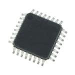
| 供应商器件封装 | 32-TQFP(7x7) |
| 其它名称 | ATMEGA168PA-AURCT |
| 包装 | 剪切带 (CT) |
| 外设 | 欠压检测/复位,POR,PWM,WDT |
| 封装/外壳 | 32-TQFP |
| 工作温度 | -40°C ~ 85°C |
| 振荡器类型 | 内部 |
| 数据转换器 | A/D 8x10b |
| 标准包装 | 1 |
| 核心处理器 | AVR |
| 核心尺寸 | 8-位 |
| 电压-电源(Vcc/Vdd) | 1.8 V ~ 5.5 V |
| 程序存储器类型 | 闪存 |
| 程序存储容量 | 16KB(8K x 16) |
| 连接性 | I²C, SPI, UART/USART |
| 速度 | 20MHz |
| 配用 | /product-detail/zh/ATSTK600-RC29/ATSTK600-RC29-ND/2050836 |


- 商务部:美国ITC正式对集成电路等产品启动337调查
- 曝三星4nm工艺存在良率问题 高通将骁龙8 Gen1或转产台积电
- 太阳诱电将投资9.5亿元在常州建新厂生产MLCC 预计2023年完工
- 英特尔发布欧洲新工厂建设计划 深化IDM 2.0 战略
- 台积电先进制程称霸业界 有大客户加持明年业绩稳了
- 达到5530亿美元!SIA预计今年全球半导体销售额将创下新高
- 英特尔拟将自动驾驶子公司Mobileye上市 估值或超500亿美元
- 三星加码芯片和SET,合并消费电子和移动部门,撤换高东真等 CEO
- 三星电子宣布重大人事变动 还合并消费电子和移动部门
- 海关总署:前11个月进口集成电路产品价值2.52万亿元 增长14.8%


PDF Datasheet 数据手册内容提取
ATmega48A/PA/88A/PA/168A/PA/328/P ATMEL 8-BIT MICROCONTROLLER WITH 4/8/16/32KBYTES IN-SYSTEM PROGRAMMABLE FLASH Features High Performance, Low Power Atmel®AVR® 8-Bit Microcontroller Family Advanced RISC Architecture ̶ 131 Powerful Instructions – Most Single Clock Cycle Execution ̶ 32 x 8 General Purpose Working Registers ̶ Fully Static Operation ̶ Up to 20 MIPS Throughput at 20MHz ̶ On-chip 2-cycle Multiplier High Endurance Non-volatile Memory Segments ̶ 4/8/16/32KBytes of In-System Self-Programmable Flash program memory ̶ 256/512/512/1KBytes EEPROM ̶ 512/1K/1K/2KBytes Internal SRAM ̶ Write/Erase Cycles: 10,000 Flash/100,000 EEPROM ̶ Data retention: 20 years at 85C/100 years at 25C(1) ̶ Optional Boot Code Section with Independent Lock Bits In-System Programming by On-chip Boot Program True Read-While-Write Operation ̶ Programming Lock for Software Security Atmel® QTouch® library support ̶ Capacitive touch buttons, sliders and wheels ̶ QTouch and QMatrix® acquisition ̶ Up to 64 sense channels Peripheral Features ̶ Two 8-bit Timer/Counters with Separate Prescaler and Compare Mode ̶ One 16-bit Timer/Counter with Separate Prescaler, Compare Mode, and Capture Mode ̶ Real Time Counter with Separate Oscillator ̶ Six PWM Channels ̶ 8-channel 10-bit ADC in TQFP and QFN/MLF package Temperature Measurement ̶ 6-channel 10-bit ADC in PDIP Package Temperature Measurement ̶ Programmable Serial USART ̶ Master/Slave SPI Serial Interface ̶ Byte-oriented 2-wire Serial Interface (Philips I2C compatible) ̶ Programmable Watchdog Timer with Separate On-chip Oscillator ̶ On-chip Analog Comparator ̶ Interrupt and Wake-up on Pin Change Atmel-8271JS-AVR- ATmega-Datasheet_11/2015
Special Microcontroller Features ̶ Power-on Reset and Programmable Brown-out Detection ̶ Internal Calibrated Oscillator ̶ External and Internal Interrupt Sources ̶ Six Sleep Modes: Idle, ADC Noise Reduction, Power-save, Power-down, Standby, and Extended Standby I/O and Packages ̶ 23 Programmable I/O Lines ̶ 28-pin PDIP, 32-lead TQFP, 28-pad QFN/MLF and 32-pad QFN/MLF Operating Voltage: ̶ 1.8 - 5.5V Temperature Range: ̶ -40C to 85C Speed Grade: ̶ 0 - 4MHz@1.8 - 5.5V, 0 - 10MHz@2.7 - 5.5.V, 0 - 20MHz @ 4.5 - 5.5V Power Consumption at 1MHz, 1.8V, 25C ̶ Active Mode: 0.2mA ̶ Power-down Mode: 0.1µA ̶ Power-save Mode: 0.75µA (Including 32kHz RTC) ATmega48A/PA/88A/PA/168A/PA/328/P [DATASHEET] 2 Atmel-8271JS-AVR- ATmega-Datasheet_11/2015
1. Pin Configurations Figure 1-1. Pinout ATmega48A/PA/88A/PA/168A/PA/328/P 32 TQFP Top View 28 PDIP D2 (INT0/PCINT18)D1 (TXD/PCINT17)D0 (RXD/PCINT16)C6 (RESET/PCINT14)C5 (ADC5/SCL/PCINT13)C4 (ADC4/SDA/PCINT12)C3 (ADC3/PCINT11)C2 (ADC2/PCINT10) PPPPPPPP (PCINT14/RESET) PC6 1 28 PC5 (ADC5/SCL/PCINT13) 3231302928272625 (PCINT16/RXD) PD0 2 27 PC4 (ADC4/SDA/PCINT12) (PCINT17/TXD) PD1 3 26 PC3 (ADC3/PCINT11) (PCINT19/OC2B/INT1) PD3 1 24 PC1 (ADC1/PCINT9) (PCINT18/INT0) PD2 4 25 PC2 (ADC2/PCINT10) (PCINT20/XCK/T0) PD4 2 23 PC0 (ADC0/PCINT8) (PCINT19/OC2B/INT1) PD3 5 24 PC1 (ADC1/PCINT9) GND 3 22 ADC7 (PCINT20/XCK/T0) PD4 6 23 PC0 (ADC0/PCINT8) VCC 4 21 GND VCC 7 22 GND GND 5 20 AREF GND 8 21 AREF VCC 6 19 ADC6 (PCINT6/XTAL1/TOSC1) PB6 9 20 AVCC (PCINT6/XTAL1/TOSC1) PB6 7 18 AVCC (PCINT7/XTAL2/TOSC2) PB7 10 19 PB5 (SCK/PCINT5) (PCINT7/XTAL2/TOSC2) PB7 8 17 PB5 (SCK/PCINT5) (PCINT21/OC0B/T1) PD5 11 18 PB4 (MISO/PCINT4) 910111213141516 (PCINT22/OC0A/AIN0) PD6 12 17 PB3 (MOSI/OC2A/PCINT3) (PCINT23/AIN1) PD7 13 16 PB2 (SS/OC1B/PCINT2) D5D6D7B0B1B2B3B4 (PCINT0/CLKO/ICP1) PB0 14 15 PB1 (OC1A/PCINT1) (PCINT21/OC0B/T1) P(PCINT22/OC0A/AIN0) P(PCINT23/AIN1) P(PCINT0/CLKO/ICP1) P(PCINT1/OC1A) P(PCINT2/SS/OC1B) P(PCINT3/OC2A/MOSI) P(PCINT4/MISO) P 28 MLF Top View 32 MLF Top View PD2 (INT0/PCINT18)PD1 (TXD/PCINT17)PD0 (RXD/PCINT16)PC6 (RESET/PCINT14)PC5 (ADC5/SCL/PCINT13)PC4 (ADC4/SDA/PCINT12)PC3 (ADC3/PCINT11) PD2 (INT0/PCINT18)PD1 (TXD/PCINT17)PD0 (RXD/PCINT16)PC6 (RESET/PCINT14)PC5 (ADC5/SCL/PCINT13)PC4 (ADC4/SDA/PCINT12)PC3 (ADC3/PCINT11)PC2 (ADC2/PCINT10) 28272625242322 3231302928272625 (PCINT19/OC2B/INT1) PD3 1 21 PC2 (ADC2/PCINT10) (PCINT19/OC2B/INT1) PD3 1 24 PC1 (ADC1/PCINT9) (PCINT20/XCK/T0) PD4 2 20 PC1 (ADC1/PCINT9) (PCINT20/XCK/T0) PD4 2 23 PC0 (ADC0/PCINT8) VCC 3 19 PC0 (ADC0/PCINT8) GND 3 22 ADC7 GND 4 18 GND VCC 4 21 GND (PCINT6/XTAL1/TOSC1) PB6 5 17 AREF GND 5 20 AREF (PCINT7/XTAL2/TOSC2) PB7 6 16 AVCC VCC 6 19 ADC6 (PCINT21/OC0B/T1) PD5 7 15 PB5 (SCK/PCINT5) (PCINT6/XTAL1/TOSC1) PB6 7 18 AVCC 891011121314 (PCINT7/XTAL2/TOSC2) PB7 8 17 PB5 (SCK/PCINT5) D6D7B0B1B2B3B4 910111213141516 NOTE: Bottom pad should be soldered to ground. (PCINT22/OC0A/AIN0) P(PCINT23/AIN1) P(PCINT0/CLKO/ICP1) P(PCINT1/OC1A) P(PCINT2/SS/OC1B) P(PCINT3/OC2A/MOSI) P(PCINT4/MISO) P NOTE: Bottom pad should be soldered to ground. (PCINT21/OC0B/T1) PD5(PCINT22/OC0A/AIN0) PD6(PCINT23/AIN1) PD7(PCINT0/CLKO/ICP1) PB0(PCINT1/OC1A) PB1(PCINT2/SS/OC1B) PB2(PCINT3/OC2A/MOSI) PB3(PCINT4/MISO) PB4 Table 1-1. 32UFBGA - Pinout ATmega48A/48PA/88A/88PA/168A/168PA 1 2 3 4 5 6 A PD2 PD1 PC6 PC4 PC2 PC1 B PD3 PD4 PD0 PC5 PC3 PC0 C GND GND ADC7 GND D VDD VDD AREF ADC6 E PB6 PD6 PB0 PB2 AVDD PB5 F PB7 PD5 PD7 PB1 PB3 PB4 ATmega48A/PA/88A/PA/168A/PA/328/P [DATASHEET] 3 Atmel-8271JS-AVR- ATmega-Datasheet_11/2015
1.1 Pin Descriptions 1.1.1 VCC Digital supply voltage. 1.1.2 GND Ground. 1.1.3 Port B (PB7:0) XTAL1/XTAL2/TOSC1/TOSC2 Port B is an 8-bit bi-directional I/O port with internal pull-up resistors (selected for each bit). The Port B output buffers have symmetrical drive characteristics with both high sink and source capability. As inputs, Port B pins that are externally pulled low will source current if the pull-up resistors are activated. The Port B pins are tri- stated when a reset condition becomes active, even if the clock is not running. Depending on the clock selection fuse settings, PB6 can be used as input to the inverting Oscillator amplifier and input to the internal clock operating circuit. Depending on the clock selection fuse settings, PB7 can be used as output from the inverting Oscillator amplifier. If the Internal Calibrated RC Oscillator is used as chip clock source, PB7...6 is used as TOSC2...1 input for the Asynchronous Timer/Counter2 if the AS2 bit in ASSR is set. The various special features of Port B are elaborated in ”Alternate Functions of Port B” on page 82 and ”System Clock and Clock Options” on page 27. 1.1.4 Port C (PC5:0) Port C is a 7-bit bi-directional I/O port with internal pull-up resistors (selected for each bit). The PC5...0 output buffers have symmetrical drive characteristics with both high sink and source capability. As inputs, Port C pins that are externally pulled low will source current if the pull-up resistors are activated. The Port C pins are tri- stated when a reset condition becomes active, even if the clock is not running. 1.1.5 PC6/RESET If the RSTDISBL Fuse is programmed, PC6 is used as an I/O pin. Note that the electrical characteristics of PC6 differ from those of the other pins of Port C. If the RSTDISBL Fuse is unprogrammed, PC6 is used as a Reset input. A low level on this pin for longer than the minimum pulse length will generate a Reset, even if the clock is not running. The minimum pulse length is given in Table 29-11 on page 305. Shorter pulses are not guaranteed to generate a Reset. The various special features of Port C are elaborated in ”Alternate Functions of Port C” on page 85.| 1.1.6 Port D (PD7:0) Port D is an 8-bit bi-directional I/O port with internal pull-up resistors (selected for each bit). The Port D output buffers have symmetrical drive characteristics with both high sink and source capability. As inputs, Port D pins that are externally pulled low will source current if the pull-up resistors are activated. The Port D pins are tri- stated when a reset condition becomes active, even if the clock is not running. The various special features of Port D are elaborated in ”Alternate Functions of Port D” on page 88. ATmega48A/PA/88A/PA/168A/PA/328/P [DATASHEET] 4 Atmel-8271JS-AVR- ATmega-Datasheet_11/2015
1.1.7 AV CC AV is the supply voltage pin for the A/D Converter, PC3:0, and ADC7:6. It should be externally connected to CC V , even if the ADC is not used. If the ADC is used, it should be connected to V through a low-pass filter. CC CC Note that PC6...4 use digital supply voltage, V . CC 1.1.8 AREF AREF is the analog reference pin for the A/D Converter. 1.1.9 ADC7:6 (TQFP and QFN/MLF Package Only) In the TQFP and QFN/MLF package, ADC7:6 serve as analog inputs to the A/D converter. These pins are powered from the analog supply and serve as 10-bit ADC channels. ATmega48A/PA/88A/PA/168A/PA/328/P [DATASHEET] 5 Atmel-8271JS-AVR- ATmega-Datasheet_11/2015
2. Overview The ATmega48A/PA/88A/PA/168A/PA/328/P is a low-power CMOS 8-bit microcontroller based on the AVR enhanced RISC architecture. By executing powerful instructions in a single clock cycle, the ATmega48A/PA/88A/PA/168A/PA/328/P achieves throughputs approaching 1 MIPS per MHz allowing the system designer to optimize power consumption versus processing speed. 2.1 Block Diagram Figure 2-1. Block Diagram D C N C G V Watchdog Power debugWIRE Timer Supervision POR / BOD & Watchdog PROGRAM Oscillator RESET LOGIC Oscillator Flash SRAM Circuits / Clock Generation CPU EEPROM AVCC AREF GND 2 8bit T/C 0 16bit T/C 1 A/D Conv. US 8bit T/C 2 Analog Internal 6 AB Comp. Bandgap AT D USART 0 SPI TWI PORT D (8) PORT B (8) PORT C (7) RESET XTAL[1..2] PD[0..7] PB[0..7] PC[0..6] ADC[6..7] The AVR core combines a rich instruction set with 32 general purpose working registers. All the 32 registers are directly connected to the Arithmetic Logic Unit (ALU), allowing two independent registers to be accessed in one single instruction executed in one clock cycle. The resulting architecture is more code efficient while achieving throughputs up to ten times faster than conventional CISC microcontrollers. ATmega48A/PA/88A/PA/168A/PA/328/P [DATASHEET] 6 Atmel-8271JS-AVR- ATmega-Datasheet_11/2015
The ATmega48A/PA/88A/PA/168A/PA/328/P provides the following features: 4K/8Kbytes of In-System Programmable Flash with Read-While-Write capabilities, 256/512/512/1Kbytes EEPROM, 512/1K/1K/2Kbytes SRAM, 23general purpose I/O lines, 32 general purpose working registers, three flexible Timer/Counters with compare modes, internal and external interrupts, a serial programmable USART, a byte-oriented 2-wire Serial Interface, an SPI serial port, a 6-channel 10-bit ADC (8 channels in TQFP and QFN/MLF packages), a programmable Watchdog Timer with internal Oscillator, and five software selectable power saving modes. The Idle mode stops the CPU while allowing the SRAM, Timer/Counters, USART, 2-wire Serial Interface, SPI port, and interrupt system to continue functioning. The Power-down mode saves the register contents but freezes the Oscillator, disabling all other chip functions until the next interrupt or hardware reset. In Power-save mode, the asynchronous timer continues to run, allowing the user to maintain a timer base while the rest of the device is sleeping. The ADC Noise Reduction mode stops the CPU and all I/O modules except asynchronous timer and ADC, to minimize switching noise during ADC conversions. In Standby mode, the crystal/resonator Oscillator is running while the rest of the device is sleeping. This allows very fast start-up combined with low power consumption. Atmel® offers the QTouch® library for embedding capacitive touch buttons, sliders and wheels functionality into AVR® microcontrollers. The patented charge-transfer signal acquisition offers robust sensing and includes fully debounced reporting of touch keys and includes Adjacent Key Suppression® (AKS™) technology for unambiguous detection of key events. The easy-to-use QTouch Suite toolchain allows you to explore, develop and debug your own touch applications. The device is manufactured using Atmel’s high density non-volatile memory technology. The On-chip ISP Flash allows the program memory to be reprogrammed In-System through an SPI serial interface, by a conventional non-volatile memory programmer, or by an On-chip Boot program running on the AVR core. The Boot program can use any interface to download the application program in the Application Flash memory. Software in the Boot Flash section will continue to run while the Application Flash section is updated, providing true Read- While-Write operation. By combining an 8-bit RISC CPU with In-System Self-Programmable Flash on a monolithic chip, the Atmel ATmega48A/PA/88A/PA/168A/PA/328/P is a powerful microcontroller that provides a highly flexible and cost effective solution to many embedded control applications. The ATmega48A/PA/88A/PA/168A/PA/328/P AVR is supported with a full suite of program and system development tools including: C Compilers, Macro Assemblers, Program Debugger/Simulators, In-Circuit Emulators, and Evaluation kits. 2.2 Comparison Between Processors The ATmega48A/PA/88A/PA/168A/PA/328/P differ only in memory sizes, boot loader support, and interrupt vector sizes. Table 2-1 summarizes the different memory and interrupt vector sizes for the devices. Table 2-1. Memory Size Summary Device Flash EEPROM RAM Interrupt Vector Size ATmega48A 4KBytes 256Bytes 512Bytes 1 instruction word/vector ATmega48PA 4KBytes 256Bytes 512Bytes 1 instruction word/vector ATmega88A 8KBytes 512Bytes 1KBytes 1 instruction word/vector ATmega88PA 8KBytes 512Bytes 1KBytes 1 instruction word/vector ATmega168A 16KBytes 512Bytes 1KBytes 2 instruction words/vector ATmega168PA 16KBytes 512Bytes 1KBytes 2 instruction words/vector ATmega328 32KBytes 1KBytes 2KBytes 2 instruction words/vector ATmega328P 32KBytes 1KBytes 2KBytes 2 instruction words/vector ATmega48A/PA/88A/PA/168A/PA/328/P [DATASHEET] 7 Atmel-8271JS-AVR- ATmega-Datasheet_11/2015
ATmega48A/PA/88A/PA/168A/PA/328/P support a real Read-While-Write Self-Programming mechanism. There is a separate Boot Loader Section, and the SPM instruction can only execute from there. In ATmega 48A/48PA there is no Read-While-Write support and no separate Boot Loader Section. The SPM instruction can execute from the entire Flash 3. Resources A comprehensive set of development tools, application notes and datasheets are available for download on http://www.atmel.com/avr. Note: 1. 4. Data Retention Reliability Qualification results show that the projected data retention failure rate is much less than 1 PPM over 20 years at 85°C or 100 years at 25°C. 5. About Code Examples This documentation contains simple code examples that briefly show how to use various parts of the device. These code examples assume that the part specific header file is included before compilation. Be aware that not all C compiler vendors include bit definitions in the header files and interrupt handling in C is compiler dependent. Please confirm with the C compiler documentation for more details. For I/O Registers located in extended I/O map, “IN”, “OUT”, “SBIS”, “SBIC”, “CBI”, and “SBI” instructions must be replaced with instructions that allow access to extended I/O. Typically “LDS” and “STS” combined with “SBRS”, “SBRC”, “SBR”, and “CBR”. 6. Capacitive Touch Sensing The Atmel® QTouch® Library provides a simple to use solution to realize touch sensitive interfaces on most Atmel AVR® microcontrollers. The QTouch Library includes support for the Atmel QTouch and Atmel QMatrix® acquisition methods. Touch sensing can be added to any application by linking the appropriate Atmel QTouch Library for the AVR Microcontroller. This is done by using a simple set of APIs to define the touch channels and sensors, and then calling the touch sensing APIs to retrieve the channel information and determine the touch sensor states. The QTouch Library is FREE and downloadable from the Atmel website at the following location: www.atmel.com/qtouchlibrary. For implementation details and other information, refer to the Atmel QTouch Library User Guide - also available for download from Atmel website. ATmega48A/PA/88A/PA/168A/PA/328/P [DATASHEET] 8 Atmel-8271JS-AVR- ATmega-Datasheet_11/2015
7. Register Summary Address Name Bit 7 Bit 6 Bit 5 Bit 4 Bit 3 Bit 2 Bit 1 Bit 0 Page (0xFF) Reserved – – – – – – – – (0xFE) Reserved – – – – – – – – (0xFD) Reserved – – – – – – – – (0xFC) Reserved – – – – – – – – (0xFB) Reserved – – – – – – – – (0xFA) Reserved – – – – – – – – (0xF9) Reserved – – – – – – – – (0xF8) Reserved – – – – – – – – (0xF7) Reserved – – – – – – – – (0xF6) Reserved – – – – – – – – (0xF5) Reserved – – – – – – – – (0xF4) Reserved – – – – – – – – (0xF3) Reserved – – – – – – – – (0xF2) Reserved – – – – – – – – (0xF1) Reserved – – – – – – – – (0xF0) Reserved – – – – – – – – (0xEF) Reserved – – – – – – – – (0xEE) Reserved – – – – – – – – (0xED) Reserved – – – – – – – – (0xEC) Reserved – – – – – – – – (0xEB) Reserved – – – – – – – – (0xEA) Reserved – – – – – – – – (0xE9) Reserved – – – – – – – – (0xE8) Reserved – – – – – – – – (0xE7) Reserved – – – – – – – – (0xE6) Reserved – – – – – – – – (0xE5) Reserved – – – – – – – – (0xE4) Reserved – – – – – – – – (0xE3) Reserved – – – – – – – – (0xE2) Reserved – – – – – – – – (0xE1) Reserved – – – – – – – – (0xE0) Reserved – – – – – – – – (0xDF) Reserved – – – – – – – – (0xDE) Reserved – – – – – – – – (0xDD) Reserved – – – – – – – – (0xDC) Reserved – – – – – – – – (0xDB) Reserved – – – – – – – – (0xDA) Reserved – – – – – – – – (0xD9) Reserved – – – – – – – – (0xD8) Reserved – – – – – – – – (0xD7) Reserved – – – – – – – – (0xD6) Reserved – – – – – – – – (0xD5) Reserved – – – – – – – – (0xD4) Reserved – – – – – – – – (0xD3) Reserved – – – – – – – – (0xD2) Reserved – – – – – – – – (0xD1) Reserved – – – – – – – – (0xD0) Reserved – – – – – – – – (0xCF) Reserved – – – – – – – – (0xCE) Reserved – – – – – – – – (0xCD) Reserved – – – – – – – – (0xCC) Reserved – – – – – – – – (0xCB) Reserved – – – – – – – – (0xCA) Reserved – – – – – – – – (0xC9) Reserved – – – – – – – – (0xC8) Reserved – – – – – – – – (0xC7) Reserved – – – – – – – – (0xC6) UDR0 USART I/O Data Register 191 (0xC5) UBRR0H USART Baud Rate Register High 195 (0xC4) UBRR0L USART Baud Rate Register Low 195 (0xC3) Reserved – – – – – – – – (0xC2) UCSR0C UMSEL01 UMSEL00 UPM01 UPM00 USBS0 UCSZ01 /UDORD0 UCSZ00 / UCPHA0 UCPOL0 193/204 (0xC1) UCSR0B RXCIE0 TXCIE0 UDRIE0 RXEN0 TXEN0 UCSZ02 RXB80 TXB80 192 ATmega48A/PA/88A/PA/168A/PA/328/P [DATASHEET] 9 Atmel-8271JS-AVR- ATmega-Datasheet_11/2015
Address Name Bit 7 Bit 6 Bit 5 Bit 4 Bit 3 Bit 2 Bit 1 Bit 0 Page (0xC0) UCSR0A RXC0 TXC0 UDRE0 FE0 DOR0 UPE0 U2X0 MPCM0 191 (0xBF) Reserved – – – – – – – – (0xBE) Reserved – – – – – – – – (0xBD) TWAMR TWAM6 TWAM5 TWAM4 TWAM3 TWAM2 TWAM1 TWAM0 – 233 (0xBC) TWCR TWINT TWEA TWSTA TWSTO TWWC TWEN – TWIE 230 (0xBB) TWDR 2-wire Serial Interface Data Register 232 (0xBA) TWAR TWA6 TWA5 TWA4 TWA3 TWA2 TWA1 TWA0 TWGCE 232 (0xB9) TWSR TWS7 TWS6 TWS5 TWS4 TWS3 – TWPS1 TWPS0 231 (0xB8) TWBR 2-wire Serial Interface Bit Rate Register 230 (0xB7) Reserved – – – – – – – (0xB6) ASSR – EXCLK AS2 TCN2UB OCR2AUB OCR2BUB TCR2AUB TCR2BUB 158 (0xB5) Reserved – – – – – – – – (0xB4) OCR2B Timer/Counter2 Output Compare Register B 157 (0xB3) OCR2A Timer/Counter2 Output Compare Register A 157 (0xB2) TCNT2 Timer/Counter2 (8-bit) 157 (0xB1) TCCR2B FOC2A FOC2B – – WGM22 CS22 CS21 CS20 156 (0xB0) TCCR2A COM2A1 COM2A0 COM2B1 COM2B0 – – WGM21 WGM20 153 (0xAF) Reserved – – – – – – – – (0xAE) Reserved – – – – – – – – (0xAD) Reserved – – – – – – – – (0xAC) Reserved – – – – – – – – (0xAB) Reserved – – – – – – – – (0xAA) Reserved – – – – – – – – (0xA9) Reserved – – – – – – – – (0xA8) Reserved – – – – – – – – (0xA7) Reserved – – – – – – – – (0xA6) Reserved – – – – – – – – (0xA5) Reserved – – – – – – – – (0xA4) Reserved – – – – – – – – (0xA3) Reserved – – – – – – – – (0xA2) Reserved – – – – – – – – (0xA1) Reserved – – – – – – – – (0xA0) Reserved – – – – – – – – (0x9F) Reserved – – – – – – – – (0x9E) Reserved – – – – – – – – (0x9D) Reserved – – – – – – – – (0x9C) Reserved – – – – – – – – (0x9B) Reserved – – – – – – – – (0x9A) Reserved – – – – – – – – (0x99) Reserved – – – – – – – – (0x98) Reserved – – – – – – – – (0x97) Reserved – – – – – – – – (0x96) Reserved – – – – – – – – (0x95) Reserved – – – – – – – – (0x94) Reserved – – – – – – – – (0x93) Reserved – – – – – – – – (0x92) Reserved – – – – – – – – (0x91) Reserved – – – – – – – – (0x90) Reserved – – – – – – – – (0x8F) Reserved – – – – – – – – (0x8E) Reserved – – – – – – – – (0x8D) Reserved – – – – – – – – (0x8C) Reserved – – – – – – – – (0x8B) OCR1BH Timer/Counter1 - Output Compare Register B High Byte 135 (0x8A) OCR1BL Timer/Counter1 - Output Compare Register B Low Byte 135 (0x89) OCR1AH Timer/Counter1 - Output Compare Register A High Byte 135 (0x88) OCR1AL Timer/Counter1 - Output Compare Register A Low Byte 135 (0x87) ICR1H Timer/Counter1 - Input Capture Register High Byte 135 (0x86) ICR1L Timer/Counter1 - Input Capture Register Low Byte 135 (0x85) TCNT1H Timer/Counter1 - Counter Register High Byte 134 (0x84) TCNT1L Timer/Counter1 - Counter Register Low Byte 134 (0x83) Reserved – – – – – – – – (0x82) TCCR1C FOC1A FOC1B – – – – – – 134 (0x81) TCCR1B ICNC1 ICES1 – WGM13 WGM12 CS12 CS11 CS10 133 (0x80) TCCR1A COM1A1 COM1A0 COM1B1 COM1B0 – – WGM11 WGM10 131 (0x7F) DIDR1 – – – – – – AIN1D AIN0D 236 (0x7E) DIDR0 – – ADC5D ADC4D ADC3D ADC2D ADC1D ADC0D 251 (0x7D) Reserved – – – – – – – – ATmega48A/PA/88A/PA/168A/PA/328/P [DATASHEET] 10 Atmel-8271JS-AVR- ATmega-Datasheet_11/2015
Address Name Bit 7 Bit 6 Bit 5 Bit 4 Bit 3 Bit 2 Bit 1 Bit 0 Page (0x7C) ADMUX REFS1 REFS0 ADLAR – MUX3 MUX2 MUX1 MUX0 248 (0x7B) ADCSRB – ACME – – – ADTS2 ADTS1 ADTS0 251 (0x7A) ADCSRA ADEN ADSC ADATE ADIF ADIE ADPS2 ADPS1 ADPS0 249 (0x79) ADCH ADC Data Register High byte 250 (0x78) ADCL ADC Data Register Low byte 250 (0x77) Reserved – – – – – – – – (0x76) Reserved – – – – – – – – (0x75) Reserved – – – – – – – – (0x74) Reserved – – – – – – – – (0x73) Reserved – – – – – – – – (0x72) Reserved – – – – – – – – (0x71) Reserved – – – – – – – – (0x70) TIMSK2 – – – – – OCIE2B OCIE2A TOIE2 157 (0x6F) TIMSK1 – – ICIE1 – – OCIE1B OCIE1A TOIE1 135 (0x6E) TIMSK0 – – – – – OCIE0B OCIE0A TOIE0 109 (0x6D) PCMSK2 PCINT23 PCINT22 PCINT21 PCINT20 PCINT19 PCINT18 PCINT17 PCINT16 74 (0x6C) PCMSK1 – PCINT14 PCINT13 PCINT12 PCINT11 PCINT10 PCINT9 PCINT8 74 (0x6B) PCMSK0 PCINT7 PCINT6 PCINT5 PCINT4 PCINT3 PCINT2 PCINT1 PCINT0 74 (0x6A) Reserved – – – – – – – – (0x69) EICRA – – – – ISC11 ISC10 ISC01 ISC00 71 (0x68) PCICR – – – – – PCIE2 PCIE1 PCIE0 (0x67) Reserved – – – – – – – – (0x66) OSCCAL Oscillator Calibration Register 37 (0x65) Reserved – – – – – – – – (0x64) PRR PRTWI PRTIM2 PRTIM0 – PRTIM1 PRSPI PRUSART0 PRADC 42 (0x63) Reserved – – – – – – – – (0x62) Reserved – – – – – – – – (0x61) CLKPR CLKPCE – – – CLKPS3 CLKPS2 CLKPS1 CLKPS0 37 (0x60) WDTCSR WDIF WDIE WDP3 WDCE WDE WDP2 WDP1 WDP0 54 0x3F (0x5F) SREG I T H S V N Z C 10 0x3E (0x5E) SPH – – – – – (SP10) 5. SP9 SP8 13 0x3D (0x5D) SPL SP7 SP6 SP5 SP4 SP3 SP2 SP1 SP0 13 0x3C (0x5C) Reserved – – – – – – – – 0x3B (0x5B) Reserved – – – – – – – – 0x3A (0x5A) Reserved – – – – – – – – 0x39 (0x59) Reserved – – – – – – – – 0x38 (0x58) Reserved – – – – – – – – 0x37 (0x57) SPMCSR SPMIE (RWWSB)5. SIGRD (RWWSRE)5. BLBSET PGWRT PGERS SPMEN 278 0x36 (0x56) Reserved – – – – – – – – 0x35 (0x55) MCUCR – BODS(6) BODSE(6) PUD – – IVSEL IVCE 45/68/91 0x34 (0x54) MCUSR – – – – WDRF BORF EXTRF PORF 54 0x33 (0x53) SMCR – – – – SM2 SM1 SM0 SE 40 0x32 (0x52) Reserved – – – – – – – – 0x31 (0x51) Reserved – – – – – – – – 0x30 (0x50) ACSR ACD ACBG ACO ACI ACIE ACIC ACIS1 ACIS0 235 0x2F (0x4F) Reserved – – – – – – – – 0x2E (0x4E) SPDR SPI Data Register 169 0x2D (0x4D) SPSR SPIF WCOL – – – – – SPI2X 168 0x2C (0x4C) SPCR SPIE SPE DORD MSTR CPOL CPHA SPR1 SPR0 167 0x2B (0x4B) GPIOR2 General Purpose I/O Register 2 26 0x2A (0x4A) GPIOR1 General Purpose I/O Register 1 26 0x29 (0x49) Reserved – – – – – – – – 0x28 (0x48) OCR0B Timer/Counter0 Output Compare Register B 0x27 (0x47) OCR0A Timer/Counter0 Output Compare Register A 0x26 (0x46) TCNT0 Timer/Counter0 (8-bit) 0x25 (0x45) TCCR0B FOC0A FOC0B – – WGM02 CS02 CS01 CS00 0x24 (0x44) TCCR0A COM0A1 COM0A0 COM0B1 COM0B0 – – WGM01 WGM00 0x23 (0x43) GTCCR TSM – – – – – PSRASY PSRSYNC 140/159 0x22 (0x42) EEARH (EEPROM Address Register High Byte) 5. 22 0x21 (0x41) EEARL EEPROM Address Register Low Byte 22 0x20 (0x40) EEDR EEPROM Data Register 22 0x1F (0x3F) EECR – – EEPM1 EEPM0 EERIE EEMPE EEPE EERE 22 0x1E (0x3E) GPIOR0 General Purpose I/O Register 0 26 0x1D (0x3D) EIMSK – – – – – – INT1 INT0 72 0x1C (0x3C) EIFR – – – – – – INTF1 INTF0 72 0x1B (0x3B) PCIFR – – – – – PCIF2 PCIF1 PCIF0 0x1A (0x3A) Reserved – – – – – – – – 0x19 (0x39) Reserved – – – – – – – – ATmega48A/PA/88A/PA/168A/PA/328/P [DATASHEET] 11 Atmel-8271JS-AVR- ATmega-Datasheet_11/2015
Address Name Bit 7 Bit 6 Bit 5 Bit 4 Bit 3 Bit 2 Bit 1 Bit 0 Page 0x18 (0x38) Reserved – – – – – – – – 0x17 (0x37) TIFR2 – – – – – OCF2B OCF2A TOV2 158 0x16 (0x36) TIFR1 – – ICF1 – – OCF1B OCF1A TOV1 136 0x15 (0x35) TIFR0 – – – – – OCF0B OCF0A TOV0 0x14 (0x34) Reserved – – – – – – – – 0x13 (0x33) Reserved – – – – – – – – 0x12 (0x32) Reserved – – – – – – – – 0x11 (0x31) Reserved – – – – – – – – 0x10 (0x30) Reserved – – – – – – – – 0x0F (0x2F) Reserved – – – – – – – – 0x0E (0x2E) Reserved – – – – – – – – 0x0D (0x2D) Reserved – – – – – – – – 0x0C (0x2C) Reserved – – – – – – – – 0x0B (0x2B) PORTD PORTD7 PORTD6 PORTD5 PORTD4 PORTD3 PORTD2 PORTD1 PORTD0 92 0x0A (0x2A) DDRD DDD7 DDD6 DDD5 DDD4 DDD3 DDD2 DDD1 DDD0 92 0x09 (0x29) PIND PIND7 PIND6 PIND5 PIND4 PIND3 PIND2 PIND1 PIND0 92 0x08 (0x28) PORTC – PORTC6 PORTC5 PORTC4 PORTC3 PORTC2 PORTC1 PORTC0 91 0x07 (0x27) DDRC – DDC6 DDC5 DDC4 DDC3 DDC2 DDC1 DDC0 91 0x06 (0x26) PINC – PINC6 PINC5 PINC4 PINC3 PINC2 PINC1 PINC0 92 0x05 (0x25) PORTB PORTB7 PORTB6 PORTB5 PORTB4 PORTB3 PORTB2 PORTB1 PORTB0 91 0x04 (0x24) DDRB DDB7 DDB6 DDB5 DDB4 DDB3 DDB2 DDB1 DDB0 91 0x03 (0x23) PINB PINB7 PINB6 PINB5 PINB4 PINB3 PINB2 PINB1 PINB0 91 0x02 (0x22) Reserved – – – – – – – – 0x01 (0x21) Reserved – – – – – – – – 0x0 (0x20) Reserved – – – – – – – – Note: 1. For compatibility with future devices, reserved bits should be written to zero if accessed. Reserved I/O memory addresses should never be written. 2. I/O Registers within the address range 0x00 - 0x1F are directly bit-accessible using the SBI and CBI instructions. In these registers, the value of single bits can be checked by using the SBIS and SBIC instructions. 3. Some of the Status Flags are cleared by writing a logical one to them. Note that, unlike most other AVRs, the CBI and SBI instructions will only operate on the specified bit, and can therefore be used on registers containing such Status Flags. The CBI and SBI instructions work with registers 0x00 to 0x1F only. 4. When using the I/O specific commands IN and OUT, the I/O addresses 0x00 - 0x3F must be used. When addressing I/O Registers as data space using LD and ST instructions, 0x20 must be added to these addresses. The ATmega48A/PA/88A/PA/168A/PA/328/P is a complex microcontroller with more peripheral units than can be supported within the 64 location reserved in Opcode for the IN and OUT instructions. For the Extended I/O space from 0x60 - 0xFF in SRAM, only the ST/STS/STD and LD/LDS/LDD instructions can be used. 5. Only valid for ATmega88A/88PA/168A/168PA/328/328P. 6. BODS and BODSE only available for picoPower devices ATmega48PA/88PA/168PA/328P ATmega48A/PA/88A/PA/168A/PA/328/P [DATASHEET] 12 Atmel-8271JS-AVR- ATmega-Datasheet_11/2015
8. Instruction Set Summary Mnemonics Operands Description Operation Flags #Clocks ARITHMETIC AND LOGIC INSTRUCTIONS ADD Rd, Rr Add two Registers Rd Rd + Rr Z,C,N,V,H 1 ADC Rd, Rr Add with Carry two Registers Rd Rd + Rr + C Z,C,N,V,H 1 ADIW Rdl,K Add Immediate to Word Rdh:Rdl Rdh:Rdl + K Z,C,N,V,S 2 SUB Rd, Rr Subtract two Registers Rd Rd - Rr Z,C,N,V,H 1 SUBI Rd, K Subtract Constant from Register Rd Rd - K Z,C,N,V,H 1 SBC Rd, Rr Subtract with Carry two Registers Rd Rd - Rr - C Z,C,N,V,H 1 SBCI Rd, K Subtract with Carry Constant from Reg. Rd Rd - K - C Z,C,N,V,H 1 SBIW Rdl,K Subtract Immediate from Word Rdh:Rdl Rdh:Rdl - K Z,C,N,V,S 2 AND Rd, Rr Logical AND Registers Rd Rd Rr Z,N,V 1 ANDI Rd, K Logical AND Register and Constant Rd Rd K Z,N,V 1 OR Rd, Rr Logical OR Registers Rd Rd v Rr Z,N,V 1 ORI Rd, K Logical OR Register and Constant Rd Rd v K Z,N,V 1 EOR Rd, Rr Exclusive OR Registers Rd Rd Rr Z,N,V 1 COM Rd One’s Complement Rd 0xFF Rd Z,C,N,V 1 NEG Rd Two’s Complement Rd 0x00 Rd Z,C,N,V,H 1 SBR Rd,K Set Bit(s) in Register Rd Rd v K Z,N,V 1 CBR Rd,K Clear Bit(s) in Register Rd Rd (0xFF - K) Z,N,V 1 INC Rd Increment Rd Rd + 1 Z,N,V 1 DEC Rd Decrement Rd Rd 1 Z,N,V 1 TST Rd Test for Zero or Minus Rd Rd Rd Z,N,V 1 CLR Rd Clear Register Rd Rd Rd Z,N,V 1 SER Rd Set Register Rd 0xFF None 1 MUL Rd, Rr Multiply Unsigned R1:R0 Rd x Rr Z,C 2 MULS Rd, Rr Multiply Signed R1:R0 Rd x Rr Z,C 2 MULSU Rd, Rr Multiply Signed with Unsigned R1:R0 Rd x Rr Z,C 2 FMUL Rd, Rr Fractional Multiply Unsigned R1:R0 (Rd x Rr) << 1 Z,C 2 FMULS Rd, Rr Fractional Multiply Signed R1:R0 (Rd x Rr) << 1 Z,C 2 FMULSU Rd, Rr Fractional Multiply Signed with Unsigned R1:R0 (Rd x Rr) << 1 Z,C 2 BRANCH INSTRUCTIONS RJMP k Relative Jump PC PC + k + 1 None 2 IJMP Indirect Jump to (Z) PC Z None 2 JMP(1) k Direct Jump PC k None 3 RCALL k Relative Subroutine Call PC PC + k + 1 None 3 ICALL Indirect Call to (Z) PC Z None 3 CALL(1) k Direct Subroutine Call PC k None 4 RET Subroutine Return PC STACK None 4 RETI Interrupt Return PC STACK I 4 CPSE Rd,Rr Compare, Skip if Equal if (Rd = Rr) PC PC + 2 or 3 None 1/2/3 CP Rd,Rr Compare Rd Rr Z, N,V,C,H 1 CPC Rd,Rr Compare with Carry Rd Rr C Z, N,V,C,H 1 CPI Rd,K Compare Register with Immediate Rd K Z, N,V,C,H 1 SBRC Rr, b Skip if Bit in Register Cleared if (Rr(b)=0) PC PC + 2 or 3 None 1/2/3 SBRS Rr, b Skip if Bit in Register is Set if (Rr(b)=1) PC PC + 2 or 3 None 1/2/3 SBIC P, b Skip if Bit in I/O Register Cleared if (P(b)=0) PC PC + 2 or 3 None 1/2/3 SBIS P, b Skip if Bit in I/O Register is Set if (P(b)=1) PC PC + 2 or 3 None 1/2/3 BRBS s, k Branch if Status Flag Set if (SREG(s) = 1) then PCPC+k + 1 None 1/2 BRBC s, k Branch if Status Flag Cleared if (SREG(s) = 0) then PCPC+k + 1 None 1/2 BREQ k Branch if Equal if (Z = 1) then PC PC + k + 1 None 1/2 BRNE k Branch if Not Equal if (Z = 0) then PC PC + k + 1 None 1/2 BRCS k Branch if Carry Set if (C = 1) then PC PC + k + 1 None 1/2 BRCC k Branch if Carry Cleared if (C = 0) then PC PC + k + 1 None 1/2 BRSH k Branch if Same or Higher if (C = 0) then PC PC + k + 1 None 1/2 BRLO k Branch if Lower if (C = 1) then PC PC + k + 1 None 1/2 BRMI k Branch if Minus if (N = 1) then PC PC + k + 1 None 1/2 BRPL k Branch if Plus if (N = 0) then PC PC + k + 1 None 1/2 BRGE k Branch if Greater or Equal, Signed if (N V= 0) then PC PC + k + 1 None 1/2 BRLT k Branch if Less Than Zero, Signed if (N V= 1) then PC PC + k + 1 None 1/2 BRHS k Branch if Half Carry Flag Set if (H = 1) then PC PC + k + 1 None 1/2 BRHC k Branch if Half Carry Flag Cleared if (H = 0) then PC PC + k + 1 None 1/2 BRTS k Branch if T Flag Set if (T = 1) then PC PC + k + 1 None 1/2 BRTC k Branch if T Flag Cleared if (T = 0) then PC PC + k + 1 None 1/2 BRVS k Branch if Overflow Flag is Set if (V = 1) then PC PC + k + 1 None 1/2 BRVC k Branch if Overflow Flag is Cleared if (V = 0) then PC PC + k + 1 None 1/2 BRIE k Branch if Interrupt Enabled if ( I = 1) then PC PC + k + 1 None 1/2 BRID k Branch if Interrupt Disabled if ( I = 0) then PC PC + k + 1 None 1/2 ATmega48A/PA/88A/PA/168A/PA/328/P [DATASHEET] 13 Atmel-8271JS-AVR- ATmega-Datasheet_11/2015
Mnemonics Operands Description Operation Flags #Clocks BIT AND BIT-TEST INSTRUCTIONS SBI P,b Set Bit in I/O Register I/O(P,b) 1 None 2 CBI P,b Clear Bit in I/O Register I/O(P,b) 0 None 2 LSL Rd Logical Shift Left Rd(n+1) Rd(n), Rd(0) 0 Z,C,N,V 1 LSR Rd Logical Shift Right Rd(n) Rd(n+1), Rd(7) 0 Z,C,N,V 1 ROL Rd Rotate Left Through Carry Rd(0)C,Rd(n+1) Rd(n),CRd(7) Z,C,N,V 1 ROR Rd Rotate Right Through Carry Rd(7)C,Rd(n) Rd(n+1),CRd(0) Z,C,N,V 1 ASR Rd Arithmetic Shift Right Rd(n) Rd(n+1), n=0...6 Z,C,N,V 1 SWAP Rd Swap Nibbles Rd(3...0)Rd(7...4),Rd(7...4)Rd(3...0) None 1 BSET s Flag Set SREG(s) 1 SREG(s) 1 BCLR s Flag Clear SREG(s) 0 SREG(s) 1 BST Rr, b Bit Store from Register to T T Rr(b) T 1 BLD Rd, b Bit load from T to Register Rd(b) T None 1 SEC Set Carry C 1 C 1 CLC Clear Carry C 0 C 1 SEN Set Negative Flag N 1 N 1 CLN Clear Negative Flag N 0 N 1 SEZ Set Zero Flag Z 1 Z 1 CLZ Clear Zero Flag Z 0 Z 1 SEI Global Interrupt Enable I 1 I 1 CLI Global Interrupt Disable I 0 I 1 SES Set Signed Test Flag S 1 S 1 CLS Clear Signed Test Flag S 0 S 1 SEV Set Twos Complement Overflow. V 1 V 1 CLV Clear Twos Complement Overflow V 0 V 1 SET Set T in SREG T 1 T 1 CLT Clear T in SREG T 0 T 1 SEH Set Half Carry Flag in SREG H 1 H 1 CLH Clear Half Carry Flag in SREG H 0 H 1 DATA TRANSFER INSTRUCTIONS MOV Rd, Rr Move Between Registers Rd Rr None 1 MOVW Rd, Rr Copy Register Word Rd+1:Rd Rr+1:Rr None 1 LDI Rd, K Load Immediate Rd K None 1 LD Rd, X Load Indirect Rd (X) None 2 LD Rd, X+ Load Indirect and Post-Inc. Rd (X), X X + 1 None 2 LD Rd, - X Load Indirect and Pre-Dec. X X - 1, Rd (X) None 2 LD Rd, Y Load Indirect Rd (Y) None 2 LD Rd, Y+ Load Indirect and Post-Inc. Rd (Y), Y Y + 1 None 2 LD Rd, - Y Load Indirect and Pre-Dec. Y Y - 1, Rd (Y) None 2 LDD Rd,Y+q Load Indirect with Displacement Rd (Y + q) None 2 LD Rd, Z Load Indirect Rd (Z) None 2 LD Rd, Z+ Load Indirect and Post-Inc. Rd (Z), Z Z+1 None 2 LD Rd, -Z Load Indirect and Pre-Dec. Z Z - 1, Rd (Z) None 2 LDD Rd, Z+q Load Indirect with Displacement Rd (Z + q) None 2 LDS Rd, k Load Direct from SRAM Rd (k) None 2 ST X, Rr Store Indirect (X) Rr None 2 ST X+, Rr Store Indirect and Post-Inc. (X) Rr, X X + 1 None 2 ST - X, Rr Store Indirect and Pre-Dec. X X - 1, (X) Rr None 2 ST Y, Rr Store Indirect (Y) Rr None 2 ST Y+, Rr Store Indirect and Post-Inc. (Y) Rr, Y Y + 1 None 2 ST - Y, Rr Store Indirect and Pre-Dec. Y Y - 1, (Y) Rr None 2 STD Y+q,Rr Store Indirect with Displacement (Y + q) Rr None 2 ST Z, Rr Store Indirect (Z) Rr None 2 ST Z+, Rr Store Indirect and Post-Inc. (Z) Rr, Z Z + 1 None 2 ST -Z, Rr Store Indirect and Pre-Dec. Z Z - 1, (Z) Rr None 2 STD Z+q,Rr Store Indirect with Displacement (Z + q) Rr None 2 STS k, Rr Store Direct to SRAM (k) Rr None 2 LPM Load Program Memory R0 (Z) None 3 LPM Rd, Z Load Program Memory Rd (Z) None 3 LPM Rd, Z+ Load Program Memory and Post-Inc Rd (Z), Z Z+1 None 3 SPM Store Program Memory (Z) R1:R0 None - IN Rd, P In Port Rd P None 1 OUT P, Rr Out Port P Rr None 1 PUSH Rr Push Register on Stack STACK Rr None 2 POP Rd Pop Register from Stack Rd STACK None 2 MCU CONTROL INSTRUCTIONS NOP No Operation None 1 SLEEP Sleep (see specific descr. for Sleep function) None 1 ATmega48A/PA/88A/PA/168A/PA/328/P [DATASHEET] 14 Atmel-8271JS-AVR- ATmega-Datasheet_11/2015
Mnemonics Operands Description Operation Flags #Clocks WDR Watchdog Reset (see specific descr. for WDR/timer) None 1 BREAK Break For On-chip Debug Only None N/A Note: 1. These instructions are only available in ATmega168PA and ATmega328P. ATmega48A/PA/88A/PA/168A/PA/328/P [DATASHEET] 15 Atmel-8271JS-AVR- ATmega-Datasheet_11/2015
9. Ordering Information 9.1 ATmega48A Speed (MHz) Power Supply (V) Ordering Code(2) Package(1) Operational Range(6) ATmega48A-AU 32A ATmega48A-AUR(5) 32A ATmega48A-CCU 32CC1 ATmega48A-CCUR(5) 32CC1 Industrial 20(3) 1.8 - 5.5 ATmega48A-MMH(4) 28M1 (-40C to 85C) ATmega48A-MMHR(4)(5) 28M1 ATmega48A-MU 32M1-A ATmega48A-MUR(5) 32M1-A ATmega48A-PU 28P3 Note: 1. This device can also be supplied in wafer form. Please contact your local Atmel sales office for detailed ordering information and minimum quantities. 2. Pb-free packaging complies to the European Directive for Restriction of Hazardous Substances (RoHS directive). Also Halide free and fully Green. 3. See ”Speed Grades” on page 303. 4. NiPdAu Lead Finish. 5. Tape & Reel. 6. Use ”ATmega48PA” on page 17, industrial (-40C to 105C) as the ATmega48A (-40C to 105C) is not presently offered. Package Type 32A 32-lead, Thin (1.0 mm) Plastic Quad Flat Package (TQFP) 32CC1 32-ball, 4 x 4 x 0.6 mm package, ball pitch 0.5 mm, Ultra Thin, Fine-Pitch Ball Grill Array (UFBGA) 28M1 28-pad, 4 x 4 x 1.0 body, Lead Pitch 0.45 mm Quad Flat No-Lead/Micro Lead Frame Package (QFN/MLF) 32M1-A 32-pad, 5 x 5 x 1.0 body, Lead Pitch 0.50 mm Quad Flat No-Lead/Micro Lead Frame Package (QFN/MLF) 28P3 28-lead, 0.300” Wide, Plastic Dual Inline Package (PDIP) ATmega48A/PA/88A/PA/168A/PA/328/P [DATASHEET] 16 Atmel-8271JS-AVR- ATmega-Datasheet_11/2015
9.2 ATmega48PA Speed (MHz)(3) Power Supply (V) Ordering Code(2) Package(1) Operational Range ATmega48PA-AU 32A ATmega48PA-AUR(5) 32A ATmega48PA-CCU 32CC1 ATmega48PA-CCUR(5) 32CC1 Industrial ATmega48PA-MMH(4) 28M1 (-40C to 85C) ATmega48PA-MMHR(4)(5) 28M1 ATmega48PA-MU 32M1-A ATmega48PA-MUR(5) 32M1-A 20 1.8 - 5.5 ATmega48PA-PU 28P3 ATmega48PA-AN 32A ATmega48PA-ANR(5) 32A ATmega48PA-MMN(4) 28M1 Industrial ATmega48PA-MMNR(4)(5) 28M1 (-40C to 105C) ATmega48PA-MN 32M1-A ATmega48PA-MNR(5) 32M1-A ATmega48PA-PN 28P3 Note: 1. This device can also be supplied in wafer form. Please contact your local Atmel sales office for detailed ordering information and minimum quantities. 2. Pb-free packaging complies to the European Directive for Restriction of Hazardous Substances (RoHS directive). Also Halide free and fully Green. 3. See ”Speed Grades” on page 303. 4. NiPdAu Lead Finish. 5. Tape & Reel. Package Type 32A 32-lead, Thin (1.0mm) Plastic Quad Flat Package (TQFP) 32CC1 32-ball, 4 x 4 x 0.6mm package, ball pitch 0.5mm, Ultra Thin, Fine-Pitch Ball Grill Array (UFBGA) 28M1 28-pad, 4 x 4 x 1.0 body, Lead Pitch 0.45mm Quad Flat No-Lead/Micro Lead Frame Package (QFN/MLF) 32M1-A 32-pad, 5 x 5 x 1.0 body, Lead Pitch 0.50mm Quad Flat No-Lead/Micro Lead Frame Package (QFN/MLF) 28P3 28-lead, 0.300” Wide, Plastic Dual Inline Package (PDIP) ATmega48A/PA/88A/PA/168A/PA/328/P [DATASHEET] 17 Atmel-8271JS-AVR- ATmega-Datasheet_11/2015
9.3 ATmega88A Speed (MHz) Power Supply (V) Ordering Code(2) Package(1) Operational Range(6) ATmega88A-AU 32A ATmega88A-AUR(5) 32A ATmega88A-CCU 32CC1 ATmega88A-CCUR(5) 32CC1 Industrial 20(3) 1.8 - 5.5 ATmega88A-MMH(4) 28M1 (-40C to 85C) ATmega88A-MMHR(4)(5) 28M1 ATmega88A-MU 32M1-A ATmega88A-MUR(5) 32M1-A ATmega88A-PU 28P3 Note: 1. This device can also be supplied in wafer form. Please contact your local Atmel sales office for detailed ordering information and minimum quantities. 2. Pb-free packaging complies to the European Directive for Restriction of Hazardous Substances (RoHS directive).Also Halide free and fully Green. 3. See ”Speed Grades” on page 303. 4. NiPdAu Lead Finish. 5. Tape & Reel. 6. Use ”ATmega88PA” on page 19, industrial (-40C to 105C) as the ATmega48A (-40C to 105C) is not presently offered. Package Type 32A 32-lead, Thin (1.0mm) Plastic Quad Flat Package (TQFP) 32CC1 32-ball, 4 x 4 x 0.6mm package, ball pitch 0.5mm, Ultra Thin, Fine-Pitch Ball Grill Array (UFBGA) 28M1 28-pad, 4 x 4 x 1.0 body, Lead Pitch 0.45mm Quad Flat No-Lead/Micro Lead Frame Package (QFN/MLF) 32M1-A 32-pad, 5 x 5 x 1.0 body, Lead Pitch 0.50mm Quad Flat No-Lead/Micro Lead Frame Package (QFN/MLF) 28P3 28-lead, 0.300” Wide, Plastic Dual Inline Package (PDIP) ATmega48A/PA/88A/PA/168A/PA/328/P [DATASHEET] 18 Atmel-8271JS-AVR- ATmega-Datasheet_11/2015
9.4 ATmega88PA Speed (MHz)(3) Power Supply (V) Ordering Code(2) Package(1) Operational Range ATmega88PA-AU 32A ATmega88PA-AUR(5) 32A ATmega88PA-CCU 32CC1 ATmega88PA-CCUR(5) 32CC1 Industrial ATmega88PA-MMH(4) 28M1 (-40C to 85C) ATmega88PA-MMHR(4)(5) 28M1 ATmega88PA-MU 32M1-A ATmega88PA-MUR(5) 32M1-A 20 1.8 - 5.5 ATmega88PA-PU 28P3 ATmega88PA-AN 32A ATmega88PA-ANR(5) 32A ATmega88PA-MMN(4) 28M1 Industrial ATmega88PA-MMNR(4)(5) 28M1 (-40C to 105C) ATmega88PA-MN 32M1-A ATmega88PA-MNR(5) 32M1-A ATmega88PA-PN 28P3 Note: 1. This device can also be supplied in wafer form. Please contact your local Atmel sales office for detailed ordering information and minimum quantities. 2. Pb-free packaging complies to the European Directive for Restriction of Hazardous Substances (RoHS directive).Also Halide free and fully Green. 3. See ”Speed Grades” on page 303. 4. NiPdAu Lead Finish. 5. Tape & Reel. Package Type 32A 32-lead, Thin (1.0mm) Plastic Quad Flat Package (TQFP) 32CC1 32-ball, 4 x 4 x 0.6mm package, ball pitch 0.5 mm, Ultra Thin, Fine-Pitch Ball Grill Array (UFBGA) 28M1 28-pad, 4 x 4 x 1.0 body, Lead Pitch 0.45 mm Quad Flat No-Lead/Micro Lead Frame Package (QFN/MLF) 32M1-A 32-pad, 5 x 5 x 1.0 body, Lead Pitch 0.50 mm Quad Flat No-Lead/Micro Lead Frame Package (QFN/MLF) 28P3 28-lead, 0.300” Wide, Plastic Dual Inline Package (PDIP) ATmega48A/PA/88A/PA/168A/PA/328/P [DATASHEET] 19 Atmel-8271JS-AVR- ATmega-Datasheet_11/2015
9.5 ATmega168A Speed (MHz)(3) Power Supply (V) Ordering Code(2) Package(1) Operational Range(6) ATmega168A-AU 32A ATmega168A-AUR(5) 32A ATmega168A-CCU 32CC1 ATmega168A-CCUR(5) 32CC1 Industrial 20 1.8 - 5.5 ATmega168A-MMH(4) 28M1 (-40C to 85C) ATmega168A-MMHR(4)(5) 28M1 ATmega168A-MU 32M1-A ATmega168A-MUR(5) 32M1-A ATmega168A-PU 28P3 Note: 1. This device can also be supplied in wafer form. Please contact your local Atmel sales office for detailed ordering information and minimum quantities. 2. Pb-free packaging complies to the European Directive for Restriction of Hazardous Substances (RoHS directive).Also Halide free and fully Green. 3. See ”Speed Grades” on page 303 4. NiPdAu Lead Finish. 5. Tape & Reel. 6. Use ”ATmega168PA” on page 21, industrial (-40C to 105C) as the ATmega48A (-40C to 105C) is not presently offered. Package Type 32A 32-lead, Thin (1.0mm) Plastic Quad Flat Package (TQFP) 32CC1 32-ball, 4 x 4 x 0.6 mm package, ball pitch 0.5mm, Ultra Thin, Fine-Pitch Ball Grill Array (UFBGA) 28M1 28-pad, 4 x 4 x 1.0 body, Lead Pitch 0.45mm Quad Flat No-Lead/Micro Lead Frame Package (QFN/MLF) 32M1-A 32-pad, 5 x 5 x 1.0 body, Lead Pitch 0.50mm Quad Flat No-Lead/Micro Lead Frame Package (QFN/MLF) 28P3 28-lead, 0.300” Wide, Plastic Dual Inline Package (PDIP) ATmega48A/PA/88A/PA/168A/PA/328/P [DATASHEET] 20 Atmel-8271JS-AVR- ATmega-Datasheet_11/2015
9.6 ATmega168PA Speed (MHz)(3) Power Supply (V) Ordering Code(2) Package(1) Operational Range ATmega168PA-AU 32A ATmega168PA-AUR(5) 32A ATmega168PA-CCU 32CC1 ATmega168PA-CCUR(5) 32CC1 Industrial 20 1.8 - 5.5 ATmega168PA-MMH(4) 28M1 (-40C to 85C) ATmega168PA-MMHR(4)(5) 28M1 ATmega168PA-MU 32M1-A ATmega168PA-MUR(5) 32M1-A ATmega168PA-PU 28P3 ATmega168PA-AN 32A ATmega168PA-ANR(5) 32A Industrial 20 1.8 - 5.5 ATmega168PA-MN 32M1-A (-40C to 105C) ATmega168PA-MNR(5) 32M1-A ATmega168PA-PN 28P3 Note: 1. This device can also be supplied in wafer form. Please contact your local Atmel sales office for detailed ordering information and minimum quantities. 2. Pb-free packaging complies to the European Directive for Restriction of Hazardous Substances (RoHS directive).Also Halide free and fully Green. 3. See ”Speed Grades” on page 303. 4. NiPdAu Lead Finish. 5. Tape & Reel. Package Type 32A 32-lead, Thin (1.0mm) Plastic Quad Flat Package (TQFP) 32CC1 32-ball, 4 x 4 x 0.6mm package, ball pitch 0.5mm, Ultra Thin, Fine-Pitch Ball Grill Array (UFBGA) 28M1 28-pad, 4 x 4 x 1.0 body, Lead Pitch 0.45mm Quad Flat No-Lead/Micro Lead Frame Package (QFN/MLF) 32M1-A 32-pad, 5 x 5 x 1.0 body, Lead Pitch 0.50mm Quad Flat No-Lead/Micro Lead Frame Package (QFN/MLF) 28P3 28-lead, 0.300” Wide, Plastic Dual Inline Package (PDIP) ATmega48A/PA/88A/PA/168A/PA/328/P [DATASHEET] 21 Atmel-8271JS-AVR- ATmega-Datasheet_11/2015
9.7 ATmega328 Speed (MHz) Power Supply (V) Ordering Code(2) Package(1) Operational Range(6) ATmega328-AU 32A ATmega328-AUR(5) 32A ATmega328-MMH(4) 28M1 Industrial 20(3) 1.8 - 5.5 ATmega328-MMHR(4)(5) 28M1 (-40C to 85C) ATmega328-MU 32M1-A ATmega328-MUR(5) 32M1-A ATmega328-PU 28P3 Note: 1. This device can also be supplied in wafer form. Please contact your local Atmel sales office for detailed ordering information and minimum quantities. 2. Pb-free packaging complies to the European Directive for Restriction of Hazardous Substances (RoHS directive).Also Halide free and fully Green. 3. See Figure 29-1 on page 303. 4. NiPdAu Lead Finish. 5. Tape & Reel 6. Use ”ATmega328P” on page 23, industrial (-40C to 105C) as the ATmega48A (-40C to 105C) is not presently offered. Package Type 32A 32-lead, Thin (1.0mm) Plastic Quad Flat Package (TQFP) 28M1 28-pad, 4 x 4 x 1.0 body, Lead Pitch 0.45mm Quad Flat No-Lead/Micro Lead Frame Package (QFN/MLF) 28P3 28-lead, 0.300” Wide, Plastic Dual Inline Package (PDIP) 32M1-A 32-pad, 5 x 5 x 1.0 body, Lead Pitch 0.50mm Quad Flat No-Lead/Micro Lead Frame Package (QFN/MLF) ATmega48A/PA/88A/PA/168A/PA/328/P [DATASHEET] 22 Atmel-8271JS-AVR- ATmega-Datasheet_11/2015
9.8 ATmega328P Speed (MHz)(3) Power Supply (V) Ordering Code(2) Package(1) Operational Range ATmega328P-AU 32A ATmega328P-AUR(5) 32A ATmega328P-MMH(4) 28M1 Industrial ATmega328P-MMHR(4)(5) 28M1 (-40C to 85C) ATmega328P-MU 32M1-A ATmega328P-MUR(5) 32M1-A 20 1.8 - 5.5 ATmega328P-PU 28P3 ATmega328P-AN 32A ATmega328P-ANR(5) 32A Industrial ATmega328P-MN 32M1-A (-40C to 105C) ATmega328P-MNR(5) 32M1-A ATmega328P-PN 28P3 Note: 1. This device can also be supplied in wafer form. Please contact your local Atmel sales office for detailed ordering information and minimum quantities. 2. Pb-free packaging complies to the European Directive for Restriction of Hazardous Substances (RoHS directive).Also Halide free and fully Green. 3. See Figure 29-1 on page 303. 4. NiPdAu Lead Finish. 5. Tape & Reel. Package Type 32A 32-lead, Thin (1.0mm) Plastic Quad Flat Package (TQFP) 28M1 28-pad, 4 x 4 x 1.0 body, Lead Pitch 0.45mm Quad Flat No-Lead/Micro Lead Frame Package (QFN/MLF) 28P3 28-lead, 0.300” Wide, Plastic Dual Inline Package (PDIP) 32M1-A 32-pad, 5 x 5 x 1.0 body, Lead Pitch 0.50mm Quad Flat No-Lead/Micro Lead Frame Package (QFN/MLF) ATmega48A/PA/88A/PA/168A/PA/328/P [DATASHEET] 23 Atmel-8271JS-AVR- ATmega-Datasheet_11/2015
10. Packaging Information 10.1 32A PIN 1 IDENTIFIER PIN 1 B e E1 E D1 D C 0°~7° A1 A2 A L COMMON DIMENSIONS (Unit of measure = mm) SYMBOL MIN NOM MAX NOTE A – – 1.20 A1 0.05 – 0.15 A2 0.95 1.00 1.05 D 8.75 9.00 9.25 D1 6.90 7.00 7.10 Note 2 E 8.75 9.00 9.25 Notes: E1 6.90 7.00 7.10 Note 2 1. This package conforms to JEDEC reference MS-026, Variation ABA. 2. Dimensions D1 and E1 do not include mold protrusion. Allowable B 0.30 – 0.45 protrusion is 0.25mm per side. Dimensions D1 and E1 are maximum C 0.09 – 0.20 plastic body size dimensions including mold mismatch. 3. Lead coplanarity is 0.10mm maximum. L 0.45 – 0.75 e 0.80 TYP 2010-10-20 TITLE DRAWING NO. REV. 32A, 32-lead, 7 x 7mm body size, 1.0mm body thickness, 32A C 0.8mm lead pitch, thin profile plastic quad flat package (TQFP) ATmega48A/PA/88A/PA/168A/PA/328/P [DATASHEET] 24 Atmel-8271JS-AVR- ATmega-Datasheet_11/2015
10.2 32CC1 1 2 3 4 5 6 0.08 A B Pin#1 ID C SIDE VIEW D D E F b1 A1 E A TOP VIEW A2 E1 e 32-Øb 1 2 3 4 5 6 F COMMON DIMENSIONS E (Unit of Measure = mm) D SYMBOL MIN NOM MAX NOTE D1 C A – – 0.60 B A1 0.12 – – e A A2 0.38 REF b 0.25 0.30 0.35 1 b1 0.25 – – 2 A1 BALL CORNER D 3.90 4.00 4.10 BOTTOM VIEW D1 2.50 BSC E 3 .90 4.00 4.10 E1 2.50 BSC Note1: Dimension “b” is measured at the maximum ball dia. in a plane parallel e 0.50 BSC to the seating plane. Note2: Dimension “b1” is the solderable surface defined by the opening of the solder resist layer. 07/06/10 TITLE GPC DRAWING NO. REV. Package Drawing Contact: 32CC1, 32-ball (6 x 6 Array), 4 x 4 x 0.6 mm packagedrawings@atmel.com package, ball pitch 0.50 mm, Ultra Thin, CAG 32CC1 B Fine-Pitch Ball Grid Array (UFBGA) ATmega48A/PA/88A/PA/168A/PA/328/P [DATASHEET] 25 Atmel-8271JS-AVR- ATmega-Datasheet_11/2015
10.3 28M1 D C 1 2 Pin 1 ID 3 E SIDE VIEW A1 TOP VIEW A y K D2 0.45 COMMON DIMENSIONS 1 (Unit of Measure = mm) 2 R 0.20 SYMBOL MIN NOM MAX NOTE 3 A 0.80 0.90 1.00 E2 A1 0.00 0.02 0.05 b 0.17 0.22 0.27 b C 0.20 REF D 3.95 4.00 4.05 D2 2.35 2.40 2.45 L E 3.95 4.00 4.05 e E2 2.35 2.40 2.45 0.4 Ref e 0.45 (4x) BOTTOM VIEW L 0.35 0.40 0.45 y 0.00 – 0.08 Note: The terminal #1 ID is a Laser-marked Feature. K 0.20 – – 10/24/08 TITLE GPC DRAWING NO. REV. Package Drawing Contact: 28M1, 28-pad, 4 x 4 x 1.0mm Body, Lead Pitch 0.45mm, packagedrawings@atmel.com 2.4 x 2.4mm Exposed Pad, Thermally Enhanced ZBV 28M1 B Plastic Very Thin Quad Flat No Lead Package (VQFN) ATmega48A/PA/88A/PA/168A/PA/328/P [DATASHEET] 26 Atmel-8271JS-AVR- ATmega-Datasheet_11/2015
10.4 32M1-A D D1 1 0 2 3 Pin 1 ID E1 E SIDE VIEW TOP VIEW A3 A2 A1 A K 0.08C COMMON DIMENSIONS P (Unit of Measure = mm) D2 SYMBOL MIN NOM MAX NOTE A 0.80 0.90 1.00 1 A1 – 0.02 0.05 P Pin #1 Notch 2 A2 – 0.65 1.00 (0.20 R) 3 A3 0.20 REF E2 b 0.18 0.23 0.30 K D 4.9 0 5.00 5.10 D1 4.7 0 4.75 4.80 D2 2.95 3.10 3.25 E 4.90 5.00 5.10 b e L E1 4.70 4.75 4.80 BOTTOM VIEW E2 2.95 3.10 3.25 e 0.50 BSC L 0.30 0.40 0.50 P – – 0.60 0 – – 12o Note: JEDEC Standard MO-220, Fig. 2 (Anvil Singulation), VHHD-2. K 0.20 – – 03/14/2014 32M1-A , 32-pad, 5 x 5 x 1.0mm Body, Lead Pitch 0.50mm, 3.10mm Exposed Pad, Micro Lead Frame Package (MLF) 32M1-A F ATmega48A/PA/88A/PA/168A/PA/328/P [DATASHEET] 27 Atmel-8271JS-AVR- ATmega-Datasheet_11/2015
10.5 28P3 D PIN 1 E1 A SEATING PLANE A1 L B2 B (4 PLACES) B1 e E COMMON DIMENSIONS 0º ~ 15º REF (Unit of Measure = mm) C SYMBOL MIN NOM MAX NOTE eB A – – 4.5724 A1 0.508 – – D 34.544 – 34.798 Note 1 E 7.620 – 8.255 E1 7.112 – 7.493 Note 1 B 0.381 – 0.533 B1 1.143 – 1.397 Note: 1. Dimensions D and E1 do not include mold Flash or Protrusion. Mold Flash or Protrusion shall not exceed 0.25mm (0.010"). B2 0.762 – 1.143 L 3.175 – 3.429 C 0.203 – 0.356 eB – – 10.160 e 2.540 TYP 09/28/01 TITLE DRAWING NO. REV. 2325 Orchard Parkway 28P3, 28-lead (0.300"/7.62mm Wide) Plastic Dual San Jose, CA 95131 Inline Package (PDIP) 28P3 B ATmega48A/PA/88A/PA/168A/PA/328/P [DATASHEET] 28 Atmel-8271JS-AVR- ATmega-Datasheet_11/2015
11. Errata 11.1 Errata ATmega48A The revision letter in this section refers to the revision of the ATmega48A device. 11.1.1 Rev K • Full swing crystal oscillator not supported • Parallel programming timing modified • Write wait delay for NVM is increased • Changed device ID 1. Full swing crystal oscillator not supported The full swing crystal oscillator functionality is not available in revision K. Problem fix/workaround Use alternative clock sources available in the device. 2. Parallel programming timing modified Previous die revision Revision K Symbol Parameter Min Typ. Max Units Min Typ. Max Units /WR Low to t RDY/BSY High 7.5 9 ms 9.8 10.5 ms WLRH_CE for Chip Erase /BS1 Valid to t 0 250 ns 0 335 ns BVDV DATA valid /OE Low to DATA t 250 ns 335 ns OLDV Valid 3 Write wait delay for NVM is increased The write delay for non-volatile memory (NVM) is increased as follows: Other revisions Revision K Symbol Minimum Wait Delay Minimum Wait Delay t 9ms 10.5ms WD_ERASE 4. Changed device ID The device ID has been modified according to the to the following: Any die revision Previous die revision Revision K Signature byte address ID (Unchanged) Device ID read via Device ID read via Part 0x000 0x001 0x002 debugWIRE debugWIRE ATmega48A 0x1E 0x92 0x05 0x920A 0x920A 11.1.2 Rev. E to J Not Sampled ATmega48A/PA/88A/PA/168A/PA/328/P [DATASHEET] 29 Atmel-8271JS-AVR- ATmega-Datasheet_11/2015
11.1.3 Rev. D • Analog MUX can be turned off when setting ACME bit • TWI Data setup time can be too short 1. Analog MUX can be turned off when setting ACME bit If the ACME (Analog Comparator Multiplexer Enabled) bit in ADCSRB is set while MUX3 in ADMUX is '1' (ADMUX[3:0]=1xxx), all MUXes are turned off until the ACME bit is cleared. Problem Fix/Workaround Clear the MUX3 bit before setting the ACME bit. 2. TWI Data setup time can be too short When running the device as a TWI slave with a system clock above 2MHz, the data setup time for the first bit after ACK may in some cases be too short. This may cause a false start or stop condition on the TWI line. Problem Fix/Workaround Insert a delay between setting TWDR and TWCR. ATmega48A/PA/88A/PA/168A/PA/328/P [DATASHEET] 30 Atmel-8271JS-AVR- ATmega-Datasheet_11/2015
11.2 Errata ATmega48PA The revision letter in this section refers to the revision of the ATmega48PA device. 11.2.1 Rev K • Full swing crystal oscillator not supported • Parallel programming timing modified • Write wait delay for NVM is increased 1. Full swing crystal oscillator not supported The full swing crystal oscillator functionality is not available in revision K. Problem fix/workaround Use alternative clock sources available in the device. 2. Parallel programming timing modified Previous die revision Revision K Symbol Parameter Min Typ. Max Units Min Typ. Max Units /WR Low to t RDY/BSY High 7.5 9 ms 9.8 10.5 ms WLRH_CE for Chip Erase /BS1 Valid to t 0 250 ns 0 335 ns BVDV DATA valid /OE Low to DATA t 250 ns 335 ns OLDV Valid 3 Write wait delay for NVM is increased The write delay for non-volatile memory (NVM) is increased as follows: Other revisions Revision K Symbol Minimum Wait Delay Minimum Wait Delay t 9ms 10.5ms WD_ERASE 11.2.2 Rev. E to J Not sampled. 11.2.3 Rev. D • Analog MUX can be turned off when setting ACME bit • TWI Data setup time can be too short 1. Analog MUX can be turned off when setting ACME bit If the ACME (Analog Comparator Multiplexer Enabled) bit in ADCSRB is set while MUX3 in ADMUX is '1' (ADMUX[3:0]=1xxx), all MU Xes are turned off until the ACME bit is cleared. Problem Fix/Workaround Clear the MUX3 bit before setting the ACME bit. 2. TWI Data setup time can be too short ATmega48A/PA/88A/PA/168A/PA/328/P [DATASHEET] 31 Atmel-8271JS-AVR- ATmega-Datasheet_11/2015
When running the device as a TWI slave with a system clock above 2MHz, the data setup time for the first bit after ACK may in some cases be too short. This may cause a false start or stop condition on the TWI line. Problem Fix/Workaround Insert a delay between setting TWDR and TWCR. 11.2.4 Rev B to C Not Sampled 11.2.5 Rev. A • Power consumption in power save modes • Startup time for the device 1. Power consumption in power save modes Power consumption in power save modes will be higher due to improper control of internal power management.48 Problem Fix/Workaround This problem will be corrected in Rev B. 2. Startup time for the device Due to implementation of a different NVM structure, the startup sequence for the device will require longer startup time. Problem Fix/Workaround There is no fix for this problem. ATmega48A/PA/88A/PA/168A/PA/328/P [DATASHEET] 32 Atmel-8271JS-AVR- ATmega-Datasheet_11/2015
11.3 Errata ATmega88A The revision letter in this section refers to the revision of the ATmega88A device. 11.3.1 Rev K • Full swing crystal oscillator not supported • Parallel programming timing modified • Write wait delay for NVM is increased • Changed device ID • Analog MUX can be turned off when setting ACME bit • TWI Data setup time can be too short 1. Full swing crystal oscillator not supported The full swing crystal oscillator functionality is not available in revision K. Problem fix/workaround Use alternative clock sources available in the device. 2. Parallel programming timing modified Previous die revision Revision K Symbol Parameter Min Typ. Max Units Min Typ. Max Units /WR Low to t RDY/BSY High 7.5 9 ms 9.8 10.5 ms WLRH_CE for Chip Erase /BS1 Valid to t 0 250 ns 0 335 ns BVDV DATA valid /OE Low to DATA t 250 ns 335 ns OLDV Valid 3 Write wait delay for NVM is increased The write delay for non-volatile memory (NVM) is increased as follows: Other revisions Revision K Symbol Minimum Wait Delay Minimum Wait Delay t 9ms 10.5ms WD_ERASE 4. Changed device ID The device ID has been modified according to the to the following: Any die revision Previous die revision Revision K Signature byte address ID (Unchanged) Device ID read via Device ID read via Part 0x000 0x001 0x002 debugWIRE debugWIRE ATmega88A 0x1E 0x93 0x0A 0x930F 0x930F 5. Analog MUX can be turned off when setting ACME bit ATmega48A/PA/88A/PA/168A/PA/328/P [DATASHEET] 33 Atmel-8271JS-AVR- ATmega-Datasheet_11/2015
If the ACME (Analog Comparator Multiplexer Enabled) bit in ADCSRB is set while MUX3 in ADMUX is '1' (ADMUX[3:0]=1xxx), all MU Xes are turned off until the ACME bit is cleared. Problem Fix/Workaround Clear the MUX3 bit before setting the ACME bit. 6. TWI Data setup time can be too short When running the device as a TWI slave with a system clock above 2MHz, the data setup time for the first bit after ACK may in some cases be too short. This may cause a false start or stop condition on the TWI line. Problem Fix/Workaround Insert a delay between setting TWDR and TWCR. 11.3.2 Rev. G to J Not sampled. 11.3.3 Rev. F • Analog MUX can be turned off when setting ACME bit • TWI Data setup time can be too short 1. Analog MUX can be turned off when setting ACME bit If the ACME (Analog Comparator Multiplexer Enabled) bit in ADCSRB is set while MUX3 in ADMUX is '1' (ADMUX[3:0]=1xxx), all MU Xes are turned off until the ACME bit is cleared. Problem Fix/Workaround Clear the MUX3 bit before setting the ACME bit. 2. TWI Data setup time can be too short When running the device as a TWI slave with a system clock above 2MHz, the data setup time for the first bit after ACK may in some cases be too short. This may cause a false start or stop condition on the TWI line. Problem Fix/Workaround Insert a delay between setting TWDR and TWCR. 11.3.4 Rev. A to E Not Sampled. ATmega48A/PA/88A/PA/168A/PA/328/P [DATASHEET] 34 Atmel-8271JS-AVR- ATmega-Datasheet_11/2015
11.4 Errata ATmega88PA The revision letter in this section refers to the revision of the ATmega88PA device. 11.4.1 Rev K • Full swing crystal oscillator not supported • Parallel programming timing modified • Write wait delay for NVM is increased • Analog MUX can be turned off when setting ACME bit • TWI Data setup time can be too short 1. Full swing crystal oscillator not supported The full swing crystal oscillator functionality is not available in revision K. Problem fix/workaround Use alternative clock sources available in the device. 2. Parallel programming timing modified Previous die revision Revision K Symbol Parameter Min Typ. Max Units Min Typ. Max Units /WR Low to t RDY/BSY High 7.5 9 ms 9.8 10.5 ms WLRH_CE for Chip Erase /BS1 Valid to t 0 250 ns 0 335 ns BVDV DATA valid /OE Low to DATA t 250 ns 335 ns OLDV Valid 3 Write wait delay for NVM is increased The write delay for non-volatile memory (NVM) is increased as follows: Other revisions Revision K Symbol Minimum Wait Delay Minimum Wait Delay t 9ms 10.5ms WD_ERASE 4. Analog MUX can be turned off when setting ACME bit If the ACME (Analog Comparator Multiplexer Enabled) bit in ADCSRB is set while MUX3 in ADMUX is '1' (ADMUX[3:0]=1xxx), all MU Xes are turned off until the ACME bit is cleared. Problem Fix/Workaround Clear the MUX3 bit before setting the ACME bit. 5. TWI Data setup time can be too short When running the device as a TWI slave with a system clock above 2MHz, the data setup time for the first bit after ACK may in some cases be too short. This may cause a false start or stop condition on the TWI line. Problem Fix/Workaround Insert a delay between setting TWDR and TWCR. ATmega48A/PA/88A/PA/168A/PA/328/P [DATASHEET] 35 Atmel-8271JS-AVR- ATmega-Datasheet_11/2015
11.4.2 Rev. G to J Not sampled 11.4.3 Rev. F • Analog MUX can be turned off when setting ACME bit • TWI Data setup time can be too short 1. Analog MUX can be turned off when setting ACME bit If the ACME (Analog Comparator Multiplexer Enabled) bit in ADCSRB is set while MUX3 in ADMUX is '1' (ADMUX[3:0]=1xxx), all MUXes are turned off until the ACME bit is cleared. Problem Fix/Workaround Clear the MUX3 bit before setting the ACME bit. 2. TWI Data setup time can be too short When running the device as a TWI slave with a system clock above 2MHz, the data setup time for the first bit after ACK may in some cases be too short. This may cause a false start or stop condition on the TWI line. Problem Fix/Workaround Insert a delay between setting TWDR and TWCR. 11.4.4 Rev B to E Not sampled. 11.4.5 Rev. A • Power consumption in power save modes • Startup time for the device 1. Power consumption in power save modes Power consumption in power save modes will be higher due to improper control of internal power management.48 Problem Fix/Workaround This problem will be corrected in Rev B. 2. Startup time for the device Due to implementation of a different NVM structure, the startup sequence for the device will require longer startup time. Problem Fix/Workaround There is no fix for this problem. ATmega48A/PA/88A/PA/168A/PA/328/P [DATASHEET] 36 Atmel-8271JS-AVR- ATmega-Datasheet_11/2015
11.5 Errata ATmega168A The revision letter in this section refers to the revision of the ATmega168A device. 11.5.1 Rev K • Full swing crystal oscillator not supported • Parallel programming timing modified • Write wait delay for NVM is increased • Changed device ID • Analog MUX can be turned off when setting ACME bit • TWI Data setup time can be too short 1. Full swing crystal oscillator not supported The full swing crystal oscillator functionality is not available in revision K. Problem fix/workaround Use alternative clock sources available in the device. 2. Parallel programming timing modified Previous die revision Revision K Symbol Parameter Min Typ. Max Units Min Typ. Max Units /WR Low to t RDY/BSY High 7.5 9 ms 9.8 10.5 ms WLRH_CE for Chip Erase /BS1 Valid to t 0 250 ns 0 335 ns BVDV DATA valid /OE Low to DATA t 250 ns 335 ns OLDV Valid 3 Write wait delay for NVM is increased The write delay for non-volatile memory (NVM) is increased as follows: Other revisions Revision K Symbol Minimum Wait Delay Minimum Wait Delay t 9ms 10.5ms WD_ERASE 4. Changed device ID The device ID has been modified according to the to the following: Any die revision Previous die revision Revision K Signature byte address ID (Unchanged) Device ID read via Device ID read via Part 0x000 0x001 0x002 debugWIRE debugWIRE ATmega168A 0x1E 0x94 0x06 0x940B 0x940B 5. Analog MUX can be turned off when setting ACME bit ATmega48A/PA/88A/PA/168A/PA/328/P [DATASHEET] 37 Atmel-8271JS-AVR- ATmega-Datasheet_11/2015
If the ACME (Analog Comparator Multiplexer Enabled) bit in ADCSRB is set while MUX3 in ADMUX is '1' (ADMUX[3:0]=1xxx), all MU Xes are turned off until the ACME bit is cleared. Problem Fix/Workaround Clear the MUX3 bit before setting the ACME bit. 6. TWI Data setup time can be too short When running the device as a TWI slave with a system clock above 2MHz, the data setup time for the first bit after ACK may in some cases be too short. This may cause a false start or stop condition on the TWI line. Problem Fix/Workaround Insert a delay between setting TWDR and TWCR. 11.5.2 Rev. F to J Not sampled. 11.5.3 Rev. E • Analog MUX can be turned off when setting ACME bit • TWI Data setup time can be too short 1. Analog MUX can be turned off when setting ACME bit If the ACME (Analog Comparator Multiplexer Enabled) bit in ADCSRB is set while MUX3 in ADMUX is '1' (ADMUX[3:0]=1xxx), all MUXes are turned off until the ACME bit is cleared. Problem Fix/Workaround Clear the MUX3 bit before setting the ACME bit. 2. TWI Data setup time can be too short When running the device as a TWI slave with a system clock above 2MHz, the data setup time for the first bit after ACK may in some cases be too short. This may cause a false start or stop condition on the TWI line. Problem Fix/Workaround Insert a delay between setting TWDR and TWCR. 11.5.4 Rev. A to D Not sampled. ATmega48A/PA/88A/PA/168A/PA/328/P [DATASHEET] 38 Atmel-8271JS-AVR- ATmega-Datasheet_11/2015
11.6 Errata ATmega168PA The revision letter in this section refers to the revision of the ATmega168PA device. 11.6.1 Rev K • Full swing crystal oscillator not supported • Parallel programming timing modified • Write wait delay for NVM is increased • Analog MUX can be turned off when setting ACME bit • TWI Data setup time can be too short 1. Full swing crystal oscillator not supported The full swing crystal oscillator functionality is not available in revision K. Problem fix/workaround Use alternative clock sources available in the device. 2. Parallel programming timing modified Previous die revision Revision K Symbol Parameter Min Typ. Max Units Min Typ. Max Units /WR Low to t RDY/BSY High 7.5 9 ms 9.8 10.5 ms WLRH_CE for Chip Erase /BS1 Valid to t 0 250 ns 0 335 ns BVDV DATA valid /OE Low to DATA t 250 ns 335 ns OLDV Valid 3 Write wait delay for NVM is increased The write delay for non-volatile memory (NVM) is increased as follows: Other revisions Revision K Symbol Minimum Wait Delay Minimum Wait Delay t 9ms 10.5ms WD_ERASE 4. Analog MUX can be turned off when setting ACME bit If the ACME (Analog Comparator Multiplexer Enabled) bit in ADCSRB is set while MUX3 in ADMUX is '1' (ADMUX[3:0]=1xxx), all MU Xes are turned off until the ACME bit is cleared. Problem Fix/Workaround Clear the MUX3 bit before setting the ACME bit. 5. TWI Data setup time can be too short When running the device as a TWI slave with a system clock above 2MHz, the data setup time for the first bit after ACK may in some cases be too short. This may cause a false start or stop condition on the TWI line. Problem Fix/Workaround Insert a delay between setting TWDR and TWCR. ATmega48A/PA/88A/PA/168A/PA/328/P [DATASHEET] 39 Atmel-8271JS-AVR- ATmega-Datasheet_11/2015
11.6.2 Rev. F to J Not sampled. 11.6.3 Rev E • Analog MUX can be turned off when setting ACME bit • TWI Data setup time can be too short 1. Analog MUX can be turned off when setting ACME bit If the ACME (Analog Comparator Multiplexer Enabled) bit in ADCSRB is set while MUX3 in ADMUX is '1' (ADMUX[3:0]=1xxx), all MUXes are turned off until the ACME bit is cleared. Problem Fix/Workaround Clear the MUX3 bit before setting the ACME bit. 2. TWI Data setup time can be too short When running the device as a TWI slave with a system clock above 2MHz, the data setup time for the first bit after ACK may in some cases be too short. This may cause a false start or stop condition on the TWI line. Problem Fix/Workaround Insert a delay between setting TWDR and TWCR. 11.6.4 Rev A to D Not sampled. ATmega48A/PA/88A/PA/168A/PA/328/P [DATASHEET] 40 Atmel-8271JS-AVR- ATmega-Datasheet_11/2015
11.7 Errata ATmega328 The revision letter in this section refers to the revision of the ATmega328 device. 11.7.1 Rev K • Full swing crystal oscillator not supported • Parallel programming timing modified • Write wait delay for NVM is increased • Changed device ID • Analog MUX can be turned off when setting ACME bit • TWI Data setup time can be too short 1. Full swing crystal oscillator not supported The full swing crystal oscillator functionality is not available in revision K. Problem fix/workaround Use alternative clock sources available in the device. 2. Parallel programming timing modified Previous die revision Revision K Symbol Parameter Min Typ. Max Units Min Typ. Max Units /WR Low to RDY/BSY t 7.5 9 ms 9.8 10.5 ms WLRH_CE High for Chip Erase /BS1 Valid to t 0 250 ns 0 335 ns BVDV DATA valid /OE Low to t 250 ns 335 ns OLDV DATA Valid 3 Write wait delay for NVM is increased The write delay for non-volatile memory (NVM) is increased as follows: Other revisions Revision K Symbol Minimum Wait Delay Minimum Wait Delay t 9ms 10.5ms WD_ERASE 4. Changed device ID The device ID has been modified according to the to the following: Any die revision Previous die revision Revision K Signature byte address ID (Unchanged) Device ID read via Device ID read via Part 0x000 0x001 0x002 debugWIRE debugWIRE ATmega328 0x1E 0x95 0x14 0x9514 0x9516 5. Analog MUX can be turned off when setting ACME bit If the ACME (Analog Comparator Multiplexer Enabled) bit in ADCSRB is set while MUX3 in ADMUX is '1' (ADMUX[3:0]=1xxx), all MUX es are turned off until the ACME bit is cleared. ATmega48A/PA/88A/PA/168A/PA/328/P [DATASHEET] 41 Atmel-8271JS-AVR- ATmega-Datasheet_11/2015
Problem Fix/Workaround Clear the MUX3 bit before setting the ACME bit. 6. TWI Data setup time can be too short When running the device as a TWI slave with a system clock above 2MHz, the data setup time for the first bit after ACK may in some cases be too short. This may cause a false start or stop condition on the TWI line. Problem Fix/Workaround Insert a delay between setting TWDR and TWCR. 11.7.2 Rev E to J Not sampled. 11.7.3 Rev D • Analog MUX can be turned off when setting ACME bit • TWI Data setup time can be too short 1. Analog MUX can be turned off when setting ACME bit If the ACME (Analog Comparator Multiplexer Enabled) bit in ADCSRB is set while MUX3 in ADMUX is '1' (ADMUX[3:0]=1xxx), all MUX es are turned off until the ACME bit is cleared. Problem Fix/Workaround Clear the MUX3 bit before setting the ACME bit. 2. TWI Data setup time can be too short When running the device as a TWI slave with a system clock above 2MHz, the data setup time for the first bit after ACK may in some cases be too short. This may cause a false start or stop condition on the TWI line. Problem Fix/Workaround Insert a delay between setting TWDR and TWCR. 11.7.4 Rev C Not sampled. 11.7.5 Rev B • Analog MUX can be turned off when setting ACME bit • Unstable 32kHz Oscillator 1. Analog MUX can be turned off when setting ACME bit If the ACME (Analog Comparator Multiplexer Enabled) bit in ADCSRB is set while MUX3 in ADMUX is '1' (ADMUX[3:0]=1xxx), all MUXes are turned off until the ACME bit is cleared. Problem Fix/Workaround Clear the MUX3 bit before setting the ACME bit. 2. Unstable 32kHz Oscillator The 32kHz oscillator does not work as system clock. The 32kHz oscillator used as asynchronous timer is inaccurate. Problem Fix/ Workaround ATmega48A/PA/88A/PA/168A/PA/328/P [DATASHEET] 42 Atmel-8271JS-AVR- ATmega-Datasheet_11/2015
None. 11.7.6 Rev A • Analog MUX can be turned off when setting ACME bit • Unstable 32kHz Oscillator 1. Analog MUX can be turned off when setting ACME bit If the ACME (Analog Comparator Multiplexer Enabled) bit in ADCSRB is set while MUX3 in ADMUX is '1' (ADMUX[3:0]=1xxx), all MUXes are turned off until the ACME bit is cleared. Problem Fix/Workaround Clear the MUX3 bit before setting the ACME bit. 2. Unstable 32kHz Oscillator The 32kHz oscillator does not work as system clock. The 32kHz oscillator used as asynchronous timer is inaccurate. Problem Fix/ Workaround None. ATmega48A/PA/88A/PA/168A/PA/328/P [DATASHEET] 43 Atmel-8271JS-AVR- ATmega-Datasheet_11/2015
11.8 Errata ATmega328P The revision letter in this section refers to the revision of the ATmega328P device. 11.8.1 Rev K • Full swing crystal oscillator not supported • Parallel programming timing modified • Write wait delay for NVM is increased • Changed device ID • Analog MUX can be turned off when setting ACME bit • TWI Data setup time can be too short 1. Full swing crystal oscillator not supported The full swing crystal oscillator functionality is not available in revision K. Problem fix/workaround Use alternative clock sources available in the device. 2. Parallel programming timing modified Previous die revision Revision K Symbol Parameter Min Typ. Max Units Min Typ. Max Units /WR Low to RDY/BSY t 7.5 9 ms 9.8 10.5 ms WLRH_CE High for Chip Erase /BS1 Valid to t 0 250 ns 0 335 ns BVDV DATA valid /OE Low to t 250 ns 335 ns OLDV DATA Valid 3 Write wait delay for NVM is increased The write delay for non-volatile memory (NVM) is increased as follows: Other revisions Revision K Symbol Minimum Wait Delay Minimum Wait Delay t 9ms 10.5ms WD_ERASE 4. Changed device ID The device ID has been modified according to the to the following: Any die revision Previous die revision Revision K Signature byte address ID (Unchanged) Device ID read via Device ID read via Part 0x000 0x001 0x002 debugWIRE debugWIRE ATmega328P 0x1E 0x95 0x0F 0x950F 0x9516 ATmega48A/PA/88A/PA/168A/PA/328/P [DATASHEET] 44 Atmel-8271JS-AVR- ATmega-Datasheet_11/2015
5. Analog MUX can be turned off when setting ACME bit If the ACME (Analog Comparator Multiplexer Enabled) bit in ADCSRB is set while MUX3 in ADMUX is '1' (ADMUX[3:0]=1xxx), all MUX es are turned off until the ACME bit is cleared. Problem Fix/Workaround Clear the MUX3 bit before setting the ACME bit. 6. TWI Data setup time can be too short When running the device as a TWI slave with a system clock above 2MHz, the data setup time for the first bit after ACK may in some cases be too short. This may cause a false start or stop condition on the TWI line. Problem Fix/Workaround Insert a delay between setting TWDR and TWCR. 11.8.2 Rev E to J Not sampled. 11.8.3 Rev D • Analog MUX can be turned off when setting ACME bit • TWI Data setup time can be too short 1. Analog MUX can be turned off when setting ACME bit If the ACME (Analog Comparator Multiplexer Enabled) bit in ADCSRB is set while MUX3 in ADMUX is '1' (ADMUX[3:0]=1xxx), all MUXes are turned off until the ACME bit is cleared. Problem Fix/Workaround Clear the MUX3 bit before setting the ACME bit. 2. TWI Data setup time can be too short When running the device as a TWI slave with a system clock above 2MHz, the data setup time for the first bit after ACK may in some cases be too short. This may cause a false start or stop condition on the TWI line. Problem Fix/Workaround Insert a delay between setting TWDR and TWCR. 11.8.4 Rev C Not sampled. 11.8.5 Rev B • Analog MUX can be turned off when setting ACME bit • Unstable 32kHz Oscillator 1. Analog MUX can be turned off when setting ACME bit If the ACME (Analog Comparator Multiplexer Enabled) bit in ADCSRB is set while MUX3 in ADMUX is '1' (ADMUX[3:0]=1xxx), all MUXes are turned off until the ACME bit is cleared. Problem Fix/Workaround Clear the MUX3 bit before setting the ACME bit. 2. Unstable 32kHz Oscillator ATmega48A/PA/88A/PA/168A/PA/328/P [DATASHEET] 45 Atmel-8271JS-AVR- ATmega-Datasheet_11/2015
The 32kHz oscillator does not work as system clock. The 32kHz oscillator used as asynchronous timer is inaccurate. Problem Fix/ Workaround None. 11.8.6 Rev A • Unstable 32kHz Oscillator 1. Unstable 32kHz Oscillator The 32kHz oscillator does not work as system clock. The 32kHz oscillator used as asynchronous timer is inaccurate. Problem Fix/ Workaround None. ATmega48A/PA/88A/PA/168A/PA/328/P [DATASHEET] 46 Atmel-8271JS-AVR- ATmega-Datasheet_11/2015
12. Datasheet Revision History Please note that the referring page numbers in this section are referred to this document. The referring revision in this section are referring to the document revision. 12.1 Rev. 8271J – 11/2015 1. Updated errata sections: ”Errata ATmega48A” on page 632 ”Errata ATmega48PA” on page 633 ”Errata ATmega88A” on page 634 ”Errata ATmega88PA” on page 636 ”Errata ATmega168A” on page 638 ”Errata ATmega168PA” on page 640 ”Errata ATmega328” on page 642 ”Errata ATmega328P” on page 645 12.2 Rev. 8271I – 10/2014 1. Several headings have been corrected and electrical characteristics for 105°C have been structured. 12.3 Rev. 8271H – 08/2014 1. Updated text in section Section 16.9.3 ”Fast PWM Mode” on page 123 concerning compare units allowing generation of PWM waveforms (on page 126), referring to table 16-2. 2. Updated WDT Assembly code example in Section 10.10.5 ”Watchdog Timer” on page 43 (and onwards) 3. Updated footnote 1 for tables giving DC Characteristics in ”” on page 314, ”ATmega88PA DC Characteristics – Current Consumption” on page 315, ”ATmega168PA DC Characteristics – Current Consumption” on page 316 and ”ATmega328P DC Characteristics – Current Consumption” on page 316. 4. Figure 31-1 on page 318 has been updated with the correct plot. 5. Figure 31-333 on page 493 has been updated with the correct plot. 6. Changed description of external interrupt behavior in deep sleep in Section 13. ”External Interrupts” on page 70. 7. Added wait delay for t in Table 28-18 on page 296. WD_FUSE 7. Updated errata for rev A of 48PA and 88PA in Section 11.2 on page 31 and Section 11.4 on page 35. 8. Updated back page and footer according to datasheet template of 05/2014 12.4 Rev. 8271G – 02/2013 1. Added ”Electrical Characteristics (TA = -40°C to 105°C)” on page 313. 2. Added ”ATmega48PA Typical Characteristics – (TA = -40°C to 105°C)” on page 517. 3. Added ”ATmega88PA Typical Characteristics – (TA = -40°C to 105°C)” on page 540. 4. Added ”ATmega168PA Typical Characteristics – (TA = -40°C to 105°C)” on page 563. 5. Added ”ATmega328P Typical Characteristics – (TA = -40°C to 105°C)” on page 588. 12.5 Rev. 8271F – 08/2012 1. Added ”DC Characteristics” on page 299. The following tables for DC characteristics - T = -40C to 105C added: A Table 29-2 on page 300 Table 30-3 on page 315 Table 30-4 on page 316 Table 30-5 on page 316 2. Replaced the following typical characteristics by the plots that include les characteristics at “T =-40C to 105C”: A ”ATmega48PA Typical Characteristics” on page 343 ATmega48A/PA/88A/PA/168A/PA/328/P [DATASHEET] 47 Atmel-8271JS-AVR- ATmega-Datasheet_11/2015
”ATmega88PA Typical Characteristics” on page 392 ”ATmega168PA Typical Characteristics” on page 442 ”ATmega328P Typical Characteristics” on page 492 3. Removed the Power Save (Psave) maximum numbers for all devices throughout ”Electrical Characteristics – (TA = -40°C to 85°C)” on page 299. 4. Changed the powerdown maximum numbers from 8.5 and 3µA to 10 and 5µA (ATmega48PA, ATmega88PA, ATmega168PA and ATmega328P). 5. Changed the table note “Maximum values are characterized values and not test limits in production” to “Max values are test limits in production throughout ”Electrical Characteristics – (TA = -40°C to 85°C)” on page 299. 12.6 Rev. 8271E – 07/2012 1. Updated Figure 1-1 on page 3. Overlined “RESET” in 28 MLF top view and in 32 MLF top view. 2. Added EEAR9 bit to the ”EEARH and EEARL – The EEPROM Address Register” on page 22 and updated the all bit descriptions accordingly. 3. Added a footnote “EEAR9 and EEAR8 are unused bits in ATmega48A/48PA and must always be written to zero” to ”EEARH and EEARL – The EEPROM Address Register” on page 22. 4. Updated Table 18-8 on page 155, “Waveform Generation Mode Bit Description” . WGM2, WGM1 and WGM0 changed to WGM22, WGM21 and WGM20 respectively. 5. Updated ”TCCR2B – Timer/Counter Control Register B” on page 156. bit 2 (CS22) and bit 3 (WGM22) changed from R (read only) to R/W (read/write). 6. Updated the definition of fosc on page 172. fosc is the system clock frequency (not XTAL pin frequency) 7. Updated ”SPMCSR – Store Program Memory Control and Status Register” on page 261. Bit 0 renamed SPMEN and added bit 5 “SIGRD”. 8. Replaced “SELFPRGEN” by “SPMEN” throughout the whole datasheet including in the “code examples”, except in ”Program And Data Memory Lock Bits” on page 280 and in ”Fuse Bits” on page 281. 9. Updated ”Register Summary” on page 9 to include the bits: SIGRD and SPMEN in the SMPCSR register. 10. Updated the Table 30-1 on page 313. Removed the footnote. 11. Updated the footnote of the Table 29-13 on page 306. Removed the footnote “Note 2”. 12. Updated ”Errata” on page 29. Added “Errata” TWI Data setup time can be too short. 12.7 Rev. 8271D – 05/11 1. Added Atmel QTouch Sensing Capability Feature 2. Updated ”Register Description” on page 91 with PINxn as R/W. 3. Added a footnote to the PINxn, page 91. 4. Updated “Ordering Information”,”ATmega328” on page 22. Added “ATmega328-MMH” and “ATmega328-MMHR”. 5. Updated “Ordering Information”,”ATmega328P” on page 23. Added “ATmega328P-MMH” and “ATmega328P- MMHR”. 6. Added “Ordering Information” for ATmega48PA/88PA/168PA/328P @ 105C 7. Updated ”Errata ATmega328” on page 41 and ”Errata ATmega328P” on page 44 8. Updated the datasheet according to the Atmel new brand style guide. 12.8 Rev. 8271C – 08/10 1. Added 32UFBGA Pinout, Table 1-1 on page 3. 2. Updated the “SRAM Data Memory”, Figure 8-3 on page 19. 3. Updated ”Ordering Information” on page 16 with CCU and CCUR code related to “32CC1” Package drawing. 4. “32CC1” Package drawing added ”Packaging Information” on page 24. ATmega48A/PA/88A/PA/168A/PA/328/P [DATASHEET] 48 Atmel-8271JS-AVR- ATmega-Datasheet_11/2015
12.9 Rev. 8271B – 04/10 1. Updated Table 9-8 with correct value for timer oscillator at xtal2/tos2 2. Corrected use of SBIS instructions in assembly code examples. 3. Corrected BOD and BODSE bits to R/W in Section 10.11.2 on page 45, Section 12.5 on page 68 and Section 14.4 on page 91 4. Figures for bandgap characterization added, Figure 31-34 on page 335, Figure 31-81 on page 360, Figure 31-128 on page 385, Figure 31-176 on page 411, Figure 31-223 on page 435, Figure 31-271 on page 461, Figure 31-318 on page 485 and Figure 31-365 on page 510. 5. Updated ”Packaging Information” on page 24 by replacing 28M1 with a correct corresponding package. 12.10 Rev. 8271A – 12/09 1. New datasheet 8271 with merged information for ATmega48PA, ATmega88PA, ATmega168PA and ATmega48A, ATmega88A andATmega168A. Also included information on ATmega328 and ATmega328P 2 Changes done: ̶ New devices added: ATmega48A/ATmega88A/ATmega168A and ATmega328 ̶ Updated Feature Description ̶ Updated Table 2-1 on page 7 ̶ Added note for BOD Disable on page 40. ̶ Added note on BOD and BODSE in ”MCUCR – MCU Control Register” on page 91 and ”Register Description” on page 278 ̶ Added limitation information for the application ”Boot Loader Support – Read-While-Write Self- Programming” on page 263 ̶ Added limitation information for ”Program And Data Memory Lock Bits” on page 280 ̶ Added specified DC characteristics ̶ Added typical characteristics ̶ Removed exception information in ”Address Match Unit” on page 213. ATmega48A/PA/88A/PA/168A/PA/328/P [DATASHEET] 49 Atmel-8271JS-AVR- ATmega-Datasheet_11/2015
X X X X X X Atmel Corporation 1600 Technology Drive, San Jose, CA 95110 USA T: (+1)(408) 441.0311 F: (+1)(408) 436.4200 | www.atmel.com © 2015 Atmel Corporation. / Rev.: Atmel-8271JS-AVR- ATmega-Datasheet_11/2015. Atmel®, Atmel logo and combinations thereof, Enabling Unlimited Possibilities, and others are registered trademarks or trademarks of Atmel Corporation in U.S. and other countries. Other terms and product names may be trademarks of others. DISCLAIMER: The information in this document is provided in connection with Atmel products. No license, express or implied, by estoppel or otherwise, to any intellectual property right is granted by this document or in connection with the sale of Atmel products. EXCEPT AS SET FORTH IN THE ATMEL TERMS AND CONDITIONS OF SALES LOCATED ON THE ATMEL WEBSITE, ATMEL ASSUMES NO LIABILITY WHATSOEVER AND DISCLAIMS ANY EXPRESS, IMPLIED OR STATUTORY WARRANTY RELATING TO ITS PRODUCTS INCLUDING, BUT NOT LIMITED TO, THE IMPLIED WARRANTY OF MERCHANTABILITY, FITNESS FOR A PARTICULAR PURPOSE, OR NON-INFRINGEMENT. IN NO EVENT SHALL ATMEL BE LIABLE FOR ANY DIRECT, INDIRECT, CONSEQUENTIAL, PUNITIVE, SPECIAL OR INCIDENTAL DAMAGES (INCLUDING, WITHOUT LIMITATION, DAMAGES FOR LOSS AND PROFITS, BUSINESS INTERRUPTION, OR LOSS OF INFORMATION) ARISING OUT OF THE USE OR INABILITY TO USE THIS DOCUMENT, EVEN IF ATMEL HAS BEEN ADVISED OF THE POSSIBILITY OF SUCH DAMAGES. Atmel makes no representations or warranties with respect to the accuracy or completeness of the contents of this document and reserves the right to make changes to specifications and products descriptions at any time without notice. Atmel does not make any commitment to update the information contained herein. Unless specifically provided otherwise, Atmel products are not suitable for, and shall not be used in, automotive applications. Atmel products are not intended, authorized, or warranted for use as components in applications intended to support or sustain life. SAFETY-CRITICAL, MILITARY, AND AUTOMOTIVE APPLICATIONS DISCLAIMER: Atmel products are not designed for and will not be used in connection with any applications where the failure of such products would reasonably be expected to result in significant personal injury or death (“Safety-Critical Applications”) without an Atmel officer's specific written consent. Safety-Critical Applications include, without limitation, life support devices and systems, equipment or systems for the operation of nuclear facilities and weapons systems. Atmel products are not designed nor intended for use in military or aerospace applications or environments unless specifically designated by Atmel as military-grade. Atmel products are not designed nor intended for use in automotive applications unless specifically designated by Atmel as automotive-grade.
Mouser Electronics Authorized Distributor Click to View Pricing, Inventory, Delivery & Lifecycle Information: M icrochip: ATMEGA168PA-W ATMEGA168PA-D ATMEGA48PA-MU ATMEGA48PA-AU ATMEGA48PA-PU ATMEGA168PA- AU ATMEGA168PA-MU ATMEGA168PA-AUR ATMEGA168PA-CCUR ATMEGA168PA-MMHR ATMEGA168PA- MUR ATMEGA328P-AN ATMEGA328P-ANR ATMEGA328P-AUR ATMEGA328P-MN ATMEGA328P-MNR ATMEGA328P-MUR ATMEGA328P-PN ATMEGA48PA-AUR ATMEGA48PA-MMHR ATMEGA48PA-MUR ATMEGA88PA-AUR ATMEGA88PA-MMHR ATMEGA88PA-MUR ATMEGA328P-MU ATMEGA328P-AU ATMEGA328P-PU ATMEGA328P-W-11 ATMEGA88PA-MMH ATMEGA88PA-PU ATMEGA88PA-MU ATMEGA88PA-AU ATMEGA48PA-MMH ATMEGA168PA-MMH ATmega168PA-PU ATMEGA168PA-CCU ATMEGA328-AU ATMEGA328-AUR ATMEGA328-MU ATMEGA328-MUR ATMEGA328-PU ATMEGA48PA-CCU ATMEGA48PA-CCUR ATMEGA88PA-CCU ATMEGA88PA-CCUR ATMEGA168PA-AN ATMEGA168PA-ANR ATMEGA168PA-MN ATMEGA168PA-MNR ATMEGA168PA-PN ATMEGA48PA-AN ATMEGA48PA-ANR ATMEGA48PA-MMN ATMEGA48PA-MMNR ATMEGA48PA-MN ATMEGA48PA-MNR ATMEGA48PA-PN ATMEGA88PA-AN ATMEGA88PA-ANR ATMEGA88PA-MMN ATMEGA88PA-MMNR ATMEGA88PA-MMUR ATMEGA88PA-MN ATMEGA88PA-MNR ATMEGA88PA-PN ATMEGA328-MMH ATMEGA328-MMHR ATMEGA328P-MMH ATMEGA328P-MMHR