ICGOO在线商城 > 集成电路(IC) > 时钟/计时 - 时钟缓冲器,驱动器 > PI49FCT3805CQE
 Datasheet下载
- 型号: PI49FCT3805CQE
- 制造商: Pericom
- 库位|库存: xxxx|xxxx
- 要求:
| 数量阶梯 | 香港交货 | 国内含税 |
| +xxxx | $xxxx | ¥xxxx |
查看当月历史价格
查看今年历史价格
PI49FCT3805CQE产品简介:
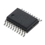
ICGOO电子元器件商城为您提供PI49FCT3805CQE由Pericom设计生产,在icgoo商城现货销售,并且可以通过原厂、代理商等渠道进行代购。 PI49FCT3805CQE价格参考¥5.49-¥5.49。PericomPI49FCT3805CQE封装/规格:时钟/计时 - 时钟缓冲器,驱动器, Clock Fanout Buffer (Distribution) IC 1:5 100MHz 20-SSOP (0.154", 3.90mm Width)。您可以下载PI49FCT3805CQE参考资料、Datasheet数据手册功能说明书,资料中有PI49FCT3805CQE 详细功能的应用电路图电压和使用方法及教程。
PI49FCT3805CQE 是由 Diodes Incorporated 生产的一款时钟缓冲器/驱动器,属于时钟与计时系列。该型号的主要应用场景包括以下方面:

1. 通信设备:
   PI49FCT3805CQE 可用于网络通信设备中,例如路由器、交换机和基站等。其高精度的时钟信号分配能力能够确保数据传输的同步性和稳定性,特别是在需要多通道时钟分发的应用中。

2. 消费电子:
   在消费类电子产品(如电视、音响系统、游戏主机等)中,该器件可以提供稳定的时钟信号,支持音频/视频同步以及系统控制功能,从而提升用户体验。

3. 计算机与外设:
   适用于台式机、笔记本电脑及其外围设备(如打印机、扫描仪等)。它能为这些设备中的处理器、存储器和其他组件提供一致且可靠的时钟信号。

4. 工业自动化:
   在工业控制系统中,例如 PLC(可编程逻辑控制器)、数据采集系统和机器人技术领域,这款时钟缓冲器可以帮助实现精确的时间同步,以保证复杂的操作流程顺畅运行。

5. 汽车电子:
   随着汽车智能化发展,车载信息娱乐系统、导航系统及驾驶辅助系统对时钟管理提出了更高要求。PI49FCT3805CQE 的高性能表现使其成为理想选择之一。

6. 医疗设备:
   在医疗器械领域,比如监护仪、超声波设备等,准确无误的时钟信号对于保障诊断结果至关重要,此产品正好满足此类需求。

总之,PI49FCT3805CQE 凭借其低抖动特性、强大的驱动能力和灵活配置选项,在众多需要高质量时钟信号分发的应用场合中发挥重要作用。
| 参数 | 数值 |
| 产品目录 | 集成电路 (IC)半导体 |
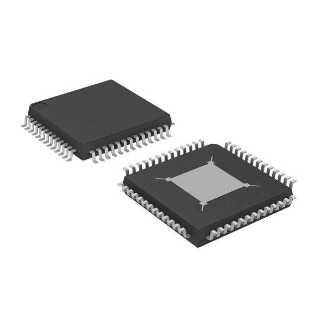
| 描述 | IC CLK BUFFER 1:5 100MHZ 20QSOP时钟缓冲器 Non Inverting Clock Driver |
| 产品分类 | |
| 品牌 | Pericom |
| 产品手册 | |
| 产品图片 | |
| rohs | 符合RoHS无铅 / 符合限制有害物质指令(RoHS)规范要求 |
| 产品系列 | 时钟和计时器IC,时钟缓冲器,Pericom PI49FCT3805CQE49FCT |
| 数据手册 | |
| 产品型号 | PI49FCT3805CQE |
| 产品培训模块 | http://www.digikey.cn/PTM/IndividualPTM.page?site=cn&lang=zhs&ptm=25951 |
| 产品种类 | 时钟缓冲器 |
| 传播延迟—最大值 | 4.5 ns |
| 供应商器件封装 | 20-QSOP |
| 包装 | 管件 |
| 商标 | Pericom |
| 安装类型 | 表面贴装 |
| 安装风格 | SMD/SMT |
| 封装 | Tube |
| 封装/外壳 | 20-SSOP(0.154",3.90mm 宽) |
| 封装/箱体 | QSOP-20 |
| 工作温度 | -40°C ~ 85°C |
| 工厂包装数量 | 55 |
| 差分-输入:输出 | 无/无 |
| 最大功率耗散 | 500 mW |
| 最大工作温度 | + 85 C |
| 最大输出频率 | 10 MHz |
| 最小工作温度 | - 40 C |
| 标准包装 | 55 |
| 比率-输入:输出 | 1:5 |
| 电压-电源 | 3 V ~ 3.6 V |
| 电源电压-最大 | 3.6 V |
| 电源电压-最小 | 3 V |
| 电源电流 | 30 uA |
| 电路数 | 2 |
| 类型 | 扇出缓冲器(分配) |
| 系列 | PI49FCT3805C |
| 输入 | CMOS,TTL |
| 输出 | CMOS |
| 输出端数量 | 10 |
| 频率-最大值 | 100MHz |


- 商务部:美国ITC正式对集成电路等产品启动337调查
- 曝三星4nm工艺存在良率问题 高通将骁龙8 Gen1或转产台积电
- 太阳诱电将投资9.5亿元在常州建新厂生产MLCC 预计2023年完工
- 英特尔发布欧洲新工厂建设计划 深化IDM 2.0 战略
- 台积电先进制程称霸业界 有大客户加持明年业绩稳了
- 达到5530亿美元!SIA预计今年全球半导体销售额将创下新高
- 英特尔拟将自动驾驶子公司Mobileye上市 估值或超500亿美元
- 三星加码芯片和SET,合并消费电子和移动部门,撤换高东真等 CEO
- 三星电子宣布重大人事变动 还合并消费电子和移动部门
- 海关总署:前11个月进口集成电路产品价值2.52万亿元 增长14.8%


PDF Datasheet 数据手册内容提取
PI49FCT3805/PI49FCT3806 3.3V Fast CMOS Buffer/Clock Driver Features Description Î 3.3V version of PI49FCT805/806 Pericom Semiconductor’s PI49FCT3805 is a 3.3V non-inverting clock driver and the PI49FCT3806 is a 3.3V inverting clock Î Extremely low output skew: 0.5ns driver designed with two independent groups of buffers. These Î Monitor ouput pin buffers have 3-state Output Enable inputs (active LOW) with a Î Clock busing wih 3-state control 1-in, 5-out configuration per group. Each clock driver consist of Î TTL input and CMOS output compatible two banks of drivers, driving five outputs each from a standard TTL compatible CMOS input. Î Industrial operation at –40°C to 85°C Î Extremely low static power (1mW, typ.) Î Hysteresis on all inputs Î Packaging (Pb-free & Green available): à 20-pin 150-mil wide QSOP (Q) à 20-pin 209-mil wide SSOP (H) PI49FCT3805 Block Diagram PI49FCT3806 Block Diagram OEA OEA 5 5 INA OA0-4 INA OA0-4 5 5 INB OB0-4 INB OB0-4 OEB OEB MON MON 11-0004 1 www.pericom.com PS7007L 07/23/10
PI49FCT3805/PI49FCT3806 3.3V Fast CMOS Buffer/Clock Driver Pin Description Pin Name Description OEA, OEB 3-State Output Enable Inputs (Active LOW) INA, INB Clock Inputs OAN, OBN Clock Outputs MON Monitor Output GND Ground VCC Power PI49FCT3805 Pin Configuration PI49FCT3805 Truth Table(1) Inputs Outputs VCCAA 1 20 VVCCCCB GONAD0 2 19 BO9B0 OEA, OEB INA, INB OAN, OBN MON OAB10 3 18 BO8B1 L L L L VOCAC2 4 17 GOBN2D L H H H GNDBA1 5 16 BG7NDB GONAD3 6 15 VOCBC3 H L Z L OBA24 7 14 BO6B4 H H Z H GNVDCCQ 8 13 GMNODN Note: OEBA3 9 12 BO5EB 1. H = High Voltage Level, L = Low Voltage Level Z = High Impedance GNINDA 10 11 BIN4B PI49FCT3806 Pin Configuration (1) PI49FCT3806 Truth Table Inputs Outputs VCCAA 1 20 VVCCCCB GONA0D 2 19 BO9B0 OEA, OEB INA, INB OAN, OBN MON OAB10 3 18 BO8B1 L L H H OVAC2C 4 17 GONBD2 L H L L GNDBA1 5 16 BG7NDB GONAD3 6 15 VOCBC3 H L Z H OAB42 7 14 BO6B4 Note: H H Z L GNVDCQC 8 13 GMNODN 1. H = High Voltage Level, L = Low Voltage Level, Z = High Impedance OEBA3 9 12 BO5EB GINNAD 10 11 BIN4B Capacitance (TA = 25°C, f = 1 MHz) Parameters(1) Description Test Conditions Typ Max. Units CIN Input Capacitance VIN = 0V 3.0 6.0 pF COUT Output Capacitance VOUT = 0V 6.0 8.0 Note: 1. This parameter is determined by device characterization but is not production tested. 11-0004 2 www.pericom.com PS7007L 07/23/10
PI49FCT3805/PI49FCT3806 3.3V Fast CMOS Buffer/Clock Driver Electrical Specifications Maximum Ratings (Above which the useful life may be impaired. For user guidelines, not tested.) Note: Storage Temperature ................................................................–65°C to +150°C Stresses greater than those listed under MAXIMUM RAT- Ambient Temperature with Power Applied ..........................–40°C to +85°C INGS may cause permanent damage to the device. This is a stress rating only and functional operation of the device Supply Voltage to Ground Potential (Inputs & Vcc Only) ....–0.5V to +7.0V at these or any other conditions above those indicated in the operational sections of this specification is not implied. Supply Voltage to Ground Potential (Outputs & I/O Only) .–0.5V to +7.0V Exposure to absolute maximum rating conditions for DC Input Voltage ........................................................................–0.5V to +7.0V extended periods may affect reliability. DC Output Current ................................................................................120 mA Power Dissipation ........................................................................................0.5W DC Electrical Characteristics (TA = –40°C to +85°C, VCC = 3.3V ±0.3V) Symbol Parameter Test Condition(1) Min. Typ. Max. Units Output High Voltage VCC = Min., IOH = -0.1mA VCC -0.2 - VOH VCC = 3.0V, VIN = VIL or VIH VIN = VIH or VIL IOH = -8mA 2.4 (3) 3.0 IOL = 0.1mA - 0.2 Output Low Voltage VCC = Min., VOL IOL = 16mA 0.2 0.4 VCC = 3.0V, VIN = VIL or VIH VIN = VIH or VIL IOL = 24mA 0.3 0.5 V Guaranteed Logic VIH Input High Voltage Input Pins 2.0 5.5 HIGH level Guaranteed Logic VIL Input Low Voltage Input Pins -0.5 0.8 LOW level VIN = VCC IIH Input High Current VCC = Max -1 1 (Input Pins) VIN = GND IIL Input Low Current VCC = Max (Input & I/O -1 1 Pins) µA High Impedance Output VCC = Max., VOUT = VCC IOZH -1 1 Current All outputs Disabled VOUT = GND High Impedance Output VCC = Max., VOUT = VCC IOZL -1 1 Current All outputs Disabled VOUT = GND VIK Clamp Diode Voltage VCC = Min., IIN = -18mA -0.7 -1.2 V IODH Output HIGH Current VVOOUUTT == 31..53VV,( 4V)IN =VIL or VIH, -35 -86 -110 IODL Output LOW Current VVOOUUTT == 31..53VV,( 4V)IN = VIL or VIH, 50 168 200 mA IOS Short Circuit(5) Current VCC = Max., VOUT = GND(5) -60 -135 -240 VH Input Hysteresis 150 mV 1. For Max. or Min. conditions, use appropriate value specified under Electrical Characteristics for the applicable device type. 2. Typical values are at VCC = 3.3V, +25°C ambient and maximum loading. 3. VOH = VCC – 0.6V at rated current. 4. This parameter is determined by device characterization but is not production tested. 5. Not more than one output should be shorted at one time. Duration of the test should not exceed one second. 11-0004 3 www.pericom.com PS7007L 07/23/10
PI49FCT3805/PI49FCT3806 3.3V Fast CMOS Buffer/Clock Driver Power Supply Characteristics (TA = –40°C to +85°C, VCC = 3.3V ±0.3V) Parameters Description Test Conditions(1) Min. Typ(2) Max. Units Quiescent Power VIN = GND or ICC VCC = Max. — 30 Supply Current VCC µA Supply Current per VIN = VCC – ΔICC Inputs @ TTL HIGH VCC = Max. 0.6V(3) — 11 300 VCC = Max., Outputs Open VIN = VCC Supply Current per OEa or OEb = GND VIN = GND mA/ ICCD Input per MHz(4) Per Output Toggling — 0.1 0.16 MHz 50% Duty Cycle VCC = Max., VIN = VCC — 3.3 9.0(5) Outputs Open VIN = GND FO = 10 MHz VIN = VCC – 50% Duty Cycle 0.6V — 3.3 10.0(5) OEA or OEB = GND VIN = GND Total Power Supply Mon. Outputs Toggling IC Current(6) VCC = Max., VIN = VCC — 1.8 6.0(5) mA Outputs Open VIN = GND fO = 2.5 MHz VIN = VCC – 50% Duty Cycle 0.6V — 1.8 7.0(5) OEa or OEb = GND VIN = GND Eleven Outputs Toggling 1. For Max. or Min. conditions, use appropriate value specified under Electrical Characteristics for the applicable device. 2. Typical values are at VCC = 3.3V, +25°C ambient. 3. Per TTL driven input (VIN = VCC – 0.6V); all other inputs at VCC or GND. 4. This parameter is not directly testable, but is derived for use in Total Power Supply Calculations. 5. Values for these conditions are examples of the Ic formula. These limits are guaranteed but not tested. 6. IC = IQUIESCENT + IINPUTS + IDYNAMIC IC = ICC + ΔICC DhNt + ICCD (fONO) ICC = Quiescent Current ΔICC = Power Supply Current for a TTL High Input (VIN = VCC – 0.6V) DH = Duty Cycle for TTL Inputs High NT = Number of TTL Inputs at DH ICCD = Dynamic Current Caused by an Input Transition Pair (HLH or LHL) fO = Output Frequency NO = Number of Outputs at fO All currents are in milliamps and all frequencies are in megahertz. 11-0004 4 www.pericom.com PS7007L 07/23/10
PI49FCT3805/PI49FCT3806 3.3V Fast CMOS Buffer/Clock Driver Switching Characteristics (TA = –40°C to +85°C, VCC = 3.3V ±0.3V) 3805 3805A 3805B 3805C 3806 3806A 3806B 3806C Test s Condi- Com. Com. Com. Com. it n Parameter Description tions(1) Min. Max. Min. Max. Min. Max. Min. Max. U Propagation Delay tPLH INA to OAN, 1.5 6.5 1.5 5.8 1.5 5.0 1.5 4.5 tPLH INB to OBN tPZH Output Enable Time 1.5 8.0 1.5 8.0 1.5 6.5 1.5 6.2 tPZL OEA to OAN, OEB to OBN tPHL Output Disable Time 1.5 7.0 1.5 7.0 1.5 6.0 1.5 5.0 tPLZ OEA to OAN, OEB to OBN CL = 50pF ns tSK(o)(3) Skew between two outputs of RL = 500Ω 0.7 0.7 0.5 0.5 same package (same transition) Skew between opposite transi- tSK(P)(3) tions (tPHL - tPLH) of the same 1.0 0.7 0.5 0.5 output Skew between two outputs of tSK(t)(3) different package at same tem- 1.5 1.2 1.0 0.8 perature (Same transition) Note: 1. See test circuit and waveforms 2. Minimum limits are guaranteed but not tested on Propagation Delays. 3. Skew measured at worst cast temperature (max. temp). (1) Tests Circuits for All Outputs Switch Position except for FIN >100 MHz Test Switch 6.0V Disable LOW 6V Enable LOW VCC Disable HIGH GND Enable HIGH 500Ω All Other Inputs Open VIN VOUT Definitions: Pulse D.U.T. CL = Load capacitance: includes jig and probe capacitance. Generator RT = Termination resistance: should be equal to ZOUT of the Pulse 50pF Generator. RT 500Ω CL 11-0004 5 www.pericom.com PS7007L 07/23/10
PI49FCT3805/PI49FCT3806 3.3V Fast CMOS Buffer/Clock Driver Switching Waveforms 3V 3V Input 1.5V Input 1.5V 0V tPLHx tPHLx 0V VOH tPLH tPHL Ox 1.5V VOH VOL Output 1.5V tSK(o) tSK(o) VOL VOH Oy 1.5V VOL Propagation Delay tPLHY tPHLy tSK(o) = | tPLHy – tPLHx | or | tPHLy – tPHLx | Enable Disable 3V Output Skew – tSK(O) OE 1.5V 0V tPZL tPLZ 3V 3.0V 3.0V Output Switch Input 1.5V Normally 1.5V Closed Low 0.3V 0V tPZH tPHZ VOL tPLH tPHL Output 0.3V VOH VOH Switch Output 1.5V Normally 1.5V Open High 0V 0V VOL tSK(p) = | tPHL – tPLH | Pulse Skew – tSK(P) Enable and Disable Times 3V Input 1.5V 0V tPLH1 tPHL1 VOH Package 1 1.5V Output VOL tSK(t) tSK(t) VOH Package 2 1.5V Output VOL tPLH2 tPHL2 tSK(t) = | tPLH2 – tPLH1 | or | tPHL2 – tPHL1 | Package Skew – tSK(t) 11-0004 6 www.pericom.com PS7007L 07/23/10
PI49FCT3805/PI49FCT3806 3.3V Fast CMOS Buffer/Clock Driver Packaging Mechanical: 20-pin SSOP (H20) 1 DATE: 04/10/08 DESCRIPTION: 20-Pin, 209-Mil Wide, SSOP PACKAGE CODE: H2 0 DOCUMENT CONTROL #: PD-1240 REVISION: E 08-0140 Note: • For latest package info, please check: http://www.pericom.com/products/packaging/mechanicals.php 11-0004 7 www.pericom.com PS7007L 07/23/10
PI49FCT3805/PI49FCT3806 3.3V Fast CMOS Buffer/Clock Driver Packaging Mechanical: 20-contact SSOP (H20) DOCUMENT CONTROL NO. PD - 1202 20 REVISION: H .00.0280 DATE: 10/22/07 MIN. .008 .150 3.81 .013 0.20 .157 3.99 0.33 Guage Plane .010 .016 0˚-6˚ 0.254 .035 1 0.41 Detail A 0.89 .337 8.56 .041 .344 8.74 1.04 REF .015 x 45˚ .058 REF 0.38 .053 1.35 1.47 .069 1.75 Detail A 1 .007 0.178 SEATING .010 0.254 PLANE .004 0.101 .025 .010 0.254 .228 BSC .008 0.203 .244 0.635 .012 0.305 5.79 6.19 X.XX DENOTES DIMENSIONS X.XX IN MILLIMETERS Pericom Semiconductor Corporation 3545 N. 1st Street, San Jose, CA 95134 1-800-435-2335 • www.pericom.com Note: 1) Controlling dimensions in inches. 2) Ref: JEDEC MO-137B/AD DESCRIPTION: 20-Pin, 150-Mil Wide, QSOP 3) Dimensions do not include mold flash, protrusions or gate burrs PACKAGE CODE: Q Note: • For latest package info, please check: http://www.pericom.com/products/packaging/mechanicals.php 11-0004 8 www.pericom.com PS7007L 07/23/10
PI49FCT3805/PI49FCT3806 3.3V Fast CMOS Buffer/Clock Driver PI49FCT3805 Ordering Information Ordering Code Package Code Speed Grade Package Description PI49FCT3805AHE H A Pb-free & Green, 20-pin 209-mil SSOP PI49FCT3805BHE H B Pb-free & Green, 20-pin 209-mil SSOP PI49FCT3805BQE Q B Pb-free & Green, 20-pin 150-mil QSOP PI49FCT3805CHE H C Pb-free & Green, 20-pin 209-mil SSOP PI49FCT3805CQE Q C Pb-free & Green, 20-pin 150-mil QSOP PI49FCT3805QE Q Blank Pb-free & Green, 20-pin 150-mil QSOP Notes: • Thermal characteristics can be found on the company web site at www.pericom.com/packaging/ • E = Pb-free and Green • Adding an X suffix = Tape/Reel PI49FCT3806 Ordering Information Ordering Code Package Code Speed Grade Package Description PI49FCT3806BQE Q B Pb-free & Green, 20-pin 150-mil QSOP Notes: • Thermal characteristics can be found on the company web site at www.pericom.com/packaging/ • E = Pb-free and Green • Adding an X suffix = Tape/Reel Pericom Semiconductor Corporation • 1-800-435-2336 11-0004 9 www.pericom.com PS7007L 07/23/10
Mouser Electronics Authorized Distributor Click to View Pricing, Inventory, Delivery & Lifecycle Information: D iodes Incorporated: PI49FCT3805CQE PI49FCT3805SE PI49FCT3805ASE PI49FCT3805CSE PI49FCT3806CQE PI49FCT3806AHE PI49FCT3806BQE PI49FCT3805ASEX PI49FCT3806QEX PI49FCT3806BQEX PI49FCT3805SEX PI49FCT3805CSEX PI49FCT3806QE PI49FCT3806CQEX PI49FCT3805BQE PI49FCT3805BQEX PI49FCT3805AQE PI49FCT3805CHE PI49FCT3805AQEX PI49FCT3805CHEX PI49FCT3805BHEX PI49FCT3805BHE PI49FCT3805QEX PI49FCT3805AHEX PI49FCT3805QE PI49FCT3805AHE PI49FCT3805CQEX PI49FCT3806AHX PI49FCT3805AHE-2017 PI49FCT3805AHEX-2017