ICGOO在线商城 > 集成电路(IC) > 时钟/计时 - 时钟缓冲器,驱动器 > CDCLVD1216RGZT

 Datasheet下载
- 型号: CDCLVD1216RGZT
- 制造商: Texas Instruments
- 库位|库存: xxxx|xxxx
- 要求:
| 数量阶梯 | 香港交货 | 国内含税 |
| +xxxx | $xxxx | ¥xxxx |
查看当月历史价格
查看今年历史价格
CDCLVD1216RGZT产品简介:
ICGOO电子元器件商城为您提供CDCLVD1216RGZT由Texas Instruments设计生产,在icgoo商城现货销售,并且可以通过原厂、代理商等渠道进行代购。 CDCLVD1216RGZT价格参考¥101.51-¥123.46。Texas InstrumentsCDCLVD1216RGZT封装/规格:时钟/计时 - 时钟缓冲器,驱动器, Clock Fanout Buffer (Distribution), Multiplexer IC 2:16 800MHz 48-VFQFN Exposed Pad。您可以下载CDCLVD1216RGZT参考资料、Datasheet数据手册功能说明书,资料中有CDCLVD1216RGZT 详细功能的应用电路图电压和使用方法及教程。
Texas Instruments(德州仪器)的CDCLVD1216RGZT是一款时钟缓冲器和驱动器,主要用于需要高性能、低抖动时钟分配的应用场景。以下是该型号的具体应用场景:

 1. 通信设备
   在通信基础设施中,如基站、路由器和交换机等设备,时钟信号的稳定性和精度至关重要。CDCLVD1216RGZT能够提供低抖动的时钟信号,确保数据传输的准确性和可靠性,特别是在高速通信协议(如以太网、PCIe等)中,它可以帮助减少误码率,提升系统的整体性能。

 2. 网络设备
   网络设备如服务器、存储系统和网络交换机等,通常需要多个同步的时钟信号来协调不同模块的工作。CDCLVD1216RGZT可以将单一输入时钟信号分配到多个输出通道,确保各个模块之间的时钟同步,避免因时钟偏差导致的数据传输错误或系统不稳定。

 3. 测试与测量仪器
   测试与测量设备(如示波器、频谱分析仪等)对时钟信号的要求极高,尤其是在高精度测量场合。CDCLVD1216RGZT的低抖动特性使其成为这些设备的理想选择,它可以为测试仪器提供稳定的参考时钟,确保测量结果的准确性。

 4. 工业自动化
   在工业控制系统中,如PLC(可编程逻辑控制器)、运动控制器等,时钟同步对于确保多个设备之间的协调工作非常重要。CDCLVD1216RGZT可以通过其多路输出功能,为不同的控制模块提供一致的时钟信号,保证系统的实时性和稳定性。

 5. 消费电子
   某些高端消费电子产品,如高清电视、蓝光播放器等,也依赖于高质量的时钟信号来实现视频和音频的同步处理。CDCLVD1216RGZT可以为这些设备提供低抖动的时钟信号,确保音视频信号的同步和清晰度。

 6. 汽车电子
   在现代汽车中,越来越多的电子系统(如ADAS、信息娱乐系统等)需要精确的时钟信号来确保各个模块的正常运行。CDCLVD1216RGZT的可靠性和低抖动特性使其适用于汽车电子领域,特别是在要求严格的车载环境中。

总之,CDCLVD1216RGZT凭借其低抖动、多通道输出和高可靠性等特点,广泛应用于各种需要高性能时钟分配的场景中,确保系统的稳定性和数据传输的准确性。
| 参数 | 数值 |
| 产品目录 | 集成电路 (IC)半导体 |
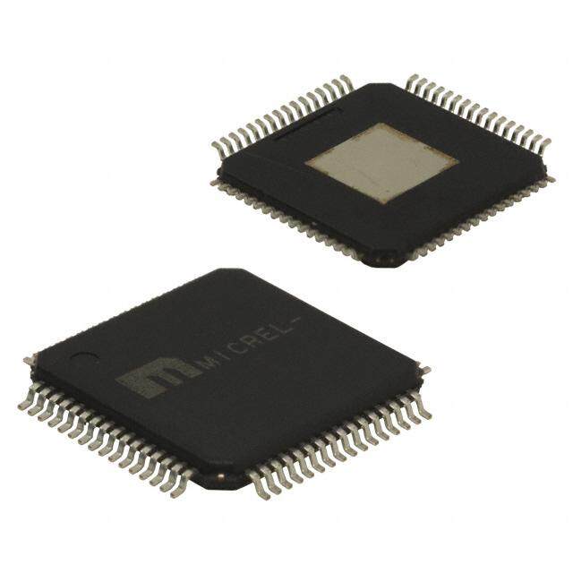
| 描述 | IC CLK BUFFER 2:16 800MHZ 48VQFN时钟缓冲器 Low Jitter,2-Inp Sel 1:16 Uni-to-LVDS Bfr |
| 产品分类 | |
| 品牌 | Texas Instruments |
| 产品手册 | |
| 产品图片 |
|
| rohs | 符合RoHS无铅 / 符合限制有害物质指令(RoHS)规范要求 |
| 产品系列 | 时钟和计时器IC,时钟缓冲器,Texas Instruments CDCLVD1216RGZT- |
| 数据手册 | 点击此处下载产品Datasheethttp://www.ti.com/lit/pdf/slyb174 |
| 产品型号 | CDCLVD1216RGZT |
| PCN封装 | |
| 产品种类 | 时钟缓冲器 |
| 传播延迟—最大值 | 2.5 ns |
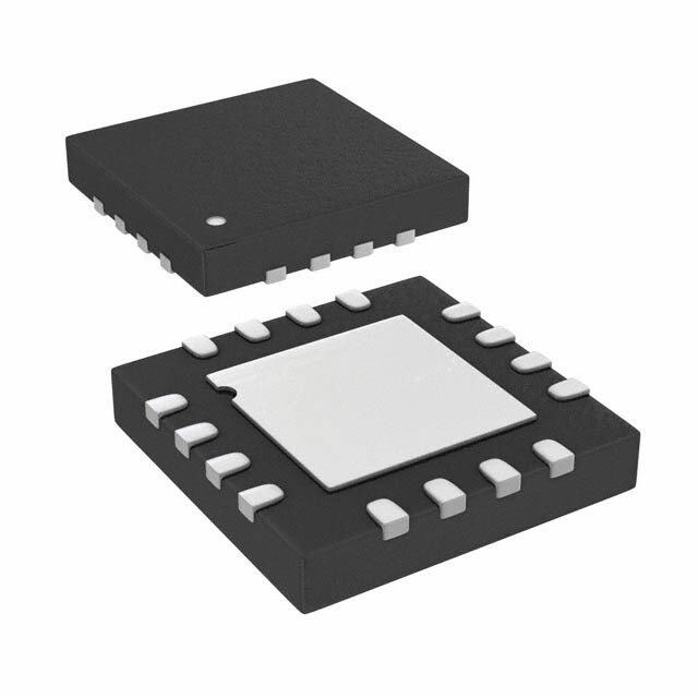
| 供应商器件封装 | 48-VQFN(7x7) |
| 其它名称 | 296-28207-1 |
| 包装 | 剪切带 (CT) |
| 商标 | Texas Instruments |
| 安装类型 | 表面贴装 |
| 安装风格 | SMD/SMT |
| 封装 | Reel |
| 封装/外壳 | 48-VFQFN 裸露焊盘 |
| 封装/箱体 | VQFN-48 |
| 工作温度 | -40°C ~ 85°C |
| 工厂包装数量 | 250 |
| 差分-输入:输出 | 是/是 |
| 最大工作温度 | + 85 C |
| 最大输入频率 | 800 MHz |
| 最小工作温度 | - 40 C |
| 标准包装 | 1 |
| 比率-输入:输出 | 2:16 |
| 电压-电源 | 2.375 V ~ 2.625 V |
| 电源电压-最大 | 2.625 V |
| 电源电压-最小 | 2.375 V |
| 电源电流 | 147 mA |
| 电路数 | 1 |
| 类型 | 扇出缓冲器(分配),多路复用器 |
| 系列 | CDCLVD1216 |
| 输入 | LVCMOS,LVDS,LVPECL |
| 输入类型 | LVCMOS, LVDS, LVPECL |
| 输出 | LVDS |
| 输出端数量 | 16 |
| 输出类型 | Differential LVDS |
| 频率-最大值 | 800MHz |


- 商务部:美国ITC正式对集成电路等产品启动337调查
- 曝三星4nm工艺存在良率问题 高通将骁龙8 Gen1或转产台积电
- 太阳诱电将投资9.5亿元在常州建新厂生产MLCC 预计2023年完工
- 英特尔发布欧洲新工厂建设计划 深化IDM 2.0 战略
- 台积电先进制程称霸业界 有大客户加持明年业绩稳了
- 达到5530亿美元!SIA预计今年全球半导体销售额将创下新高
- 英特尔拟将自动驾驶子公司Mobileye上市 估值或超500亿美元
- 三星加码芯片和SET,合并消费电子和移动部门,撤换高东真等 CEO
- 三星电子宣布重大人事变动 还合并消费电子和移动部门
- 海关总署:前11个月进口集成电路产品价值2.52万亿元 增长14.8%


PDF Datasheet 数据手册内容提取
CDCLVD1216 www.ti.com SCAS900B–OCTOBER2010–REVISEDJANUARY2011 2:16 Low Additive Jitter LVDS Buffer CheckforSamples:CDCLVD1216 FEATURES 1 DESCRIPTION • 2:16DifferentialBuffer The CDCLVD1216 clock buffer distributes one of two • LowAdditiveJitter: <300fsRMSin selectable clock inputs (IN0, IN1) to 16 pairs of 10kHzto20MHz differential LVDS clock outputs (OUT0, OUT15) with • LowOutputSkewof55ps(Max) minimum skew for clock distribution. The • UniversalInputsAcceptLVDS,LVPECL, CDCLVD1216 can accept two clock sources into an LVCMOS input multiplexer. The inputs can either be LVDS, LVPECL,orLVCMOS. • SelectableClockInputsThroughControlPin The CDCLVD1216 is specifically designed for driving • 16LVDSOutputs,ANSIEIA/TIA-644AStandard 50 Ω transmission lines. If driving the inputs in single Compatible ended mode, the appropriate bias voltage (V ) AC_REF • ClockFrequencyupto800MHz shouldbeappliedtotheunusednegativeinputpin. • 2.375–2.625VDevicePowerSupply The IN_SEL pin selects the input which is routed to • LVDSReferenceVoltage,VAC_REF,Availablefor the outputs. If this pin is left open it disables the CapacitiveCoupledInputs outputs (static). The part supports a fail safe function. • IndustrialTemperatureRange –40°Cto85°C It incorporates an input hysteresis, which prevents random oscillation of the outputs in absence of an • Packagedin7mm ×7mm48-PinQFN(RGZ) inputsignal. • ESDProtectionExceeds3kVHBM,1kVCDM The device operates in 2.5 V supply environment and is characterized from –40°C to 85°C (ambient APPLICATIONS temperature). The CDCLVD1216 is packaged in • Telecommunications/Networking small48-pin,7mm×7mmQFNpackage. • MedicalImaging • TestandMeasurementEquipment • WirelessCommunications • GeneralPurposeClocking 125MHz 125MHz PPPHHHYY2Y22 PHY2 Oscillator CDCLVD1216 PPPHHHY2YY222 LVDS Buffer PHY16 IN_SEL Figure1. ApplicationExample 1 Pleasebeawarethatanimportantnoticeconcerningavailability,standardwarranty,anduseincriticalapplicationsof TexasInstrumentssemiconductorproductsanddisclaimerstheretoappearsattheendofthisdatasheet. PRODUCTIONDATAinformationiscurrentasofpublicationdate. Copyright©2010–2011,TexasInstrumentsIncorporated Products conform to specifications per the terms of the Texas Instruments standard warranty. Production processing does not necessarilyincludetestingofallparameters.
CDCLVD1216 SCAS900B–OCTOBER2010–REVISEDJANUARY2011 www.ti.com Thesedeviceshavelimitedbuilt-inESDprotection.Theleadsshouldbeshortedtogetherorthedeviceplacedinconductivefoam duringstorageorhandlingtopreventelectrostaticdamagetotheMOSgates. V V V V V V CC CC CC CC CC CC V AC_REF0 Reference V Generator AC_REF1 INP0 INN0 X OUTP [0..15] U M LVDS INP1 N_ OUTN [0..15] I INN1 V CC 200 kW IN_SEL 200 kW GND GND Figure2. CDCLVD1216BlockDiagram CDCLVD1216 (TOPVIEW) 0 0 1 1 9 9 8 8 7 7 6 6 5 5 N P N P N P N P N P N P T T T T T T T T T T T T U U U U U U U U U U U U O O O O O O O O O O O O 36 35 34 33 32 31 30 29 28 27 26 25 VCC 37 24 VCC OUTP11 38 23 OUTN4 7mm x7mm OUTN11 39 48pin QFN(RGZ) 22 OUTP4 OUTP12 40 21 OUTN3 OUTN12 41 20 OUTP3 OUTP13 42 19 OUTN2 OUTN13 43 18 OUTP2 OUTP14 44 17 OUTN1 OUTN14 45 16 OUTP1 OUTP15 46 15 OUTN0 Thermal Pad(GND) OUTN15 47 14 OUTP0 VCC 48 13 VCC 1 2 3 4 5 6 7 8 9 10 11 12 GND IN_SEL INP1 INN1 VAC_REF1 VCC VCC VAC_REF0 INN0 INP0 N.C. GND 2 SubmitDocumentationFeedback Copyright©2010–2011,TexasInstrumentsIncorporated ProductFolderLinks:CDCLVD1216
CDCLVD1216 www.ti.com SCAS900B–OCTOBER2010–REVISEDJANUARY2011 PINFUNCTIONS PIN NAME NO. TYPE DESCRIPTION 6,7,13, V Power 2.5Vsuppliesforthedevice CC 24,37,48 GND 1,12 Ground Deviceground INP0,INN0 10,9 Input Differentialinputpairorsingleendedinput INP1,INN1 3,4 Input Differentialredundantinputpairorsingleendedinput OUTP0,OUTN0 14,15 Output DifferentialLVDSoutputpairno.0 OUTP1,OUTN1 16,17 Output DifferentialLVDSoutputpairno.1 OUTP2,OUTN2 18,19 Output DifferentialLVDSoutputpairno.2 OUTP3,OUTN3 20,21 Output DifferentialLVDSoutputpairno.3 OUTP4,OUTN4 22,23 Output DifferentialLVDSoutputpairno.4 OUTP5,OUTN5 25,26 Output DifferentialLVDSoutputpairno.5 OUTP6,OUTN6 27,28 Output DifferentialLVDSoutputpairno.6 OUTP7,OUTN7 29,30 Output DifferentialLVDSoutputpairno.7 OUTP8,OUTN8 31,32 Output DifferentialLVDSoutputpairno.8 OUTP9,OUTN9 33,34 Output DifferentialLVDSoutputpairno.9 OUTP10,OUTN10 35,36 Output DifferentialLVDSoutputpairno.10 OUTP11,OUTN11 38,39 Output DifferentialLVDSoutputpairno.11 OUTP12,OUTN12 40,41 Output DifferentialLVDSoutputpairno.12 OUTP13,OUTN13 42,43 Output DifferentialLVDSoutputpairno.13 OUTP14,OUTN14 44,45 Output DifferentialLVDSoutputpairno.14 OUTP15,OUTN15 46,47 Output DifferentialLVDSoutputpairno.15 Biasvoltageoutputforcapacitivecoupledinputs.Ifused,itisrecommendedtouse V 8 Output AC_REF0 a0.1µFtoGNDonthispin. Biasvoltageoutputforcapacitivecoupledinputs.Ifused,itisrecommendedtouse V 5 Output AC_REF1 a0.1µFtoGNDonthispin. N.C. 11 Noconnect Inputwithan internal200kΩ IN_SEL 2 Inputselection–selectsinputport;(SeeTable1) pull-upandpull- down Deviceground.ThermalPadmustbesolderedtoground.Seethermalmanagement ThermalPad Ground recommendations. Table1.InputSelectionTable IN_SEL ACTIVECLOCKINPUT 0 INP0,INN0 1 INP1,INN1 Open None(1) (1) Theinputbuffersaredisabledandtheoutputsarestatic. Copyright©2010–2011,TexasInstrumentsIncorporated SubmitDocumentationFeedback 3 ProductFolderLinks:CDCLVD1216
CDCLVD1216 SCAS900B–OCTOBER2010–REVISEDJANUARY2011 www.ti.com ABSOLUTE MAXIMUM RATINGS overoperatingfree-airtemperaturerange(unlessotherwisenoted) (1) VALUE UNIT Supplyvoltagerange,V –0.3to2.8 V CC Inputvoltagerange,V –0.2to(V +0.2) V I CC Outputvoltagerange,V –0.2to(V +0.2) V O CC Drivershortcircuitcurrent,I SeeNote (2) OSD Electrostaticdischarge(HumanBodyModel,1.5kΩ,100pF) >3000 V (1) Stressesbeyondthoselistedunder“absolutemaximumratings”maycausepermanentdamagetothedevice.Thesearestressratings onlyandfunctionaloperationofthedeviceattheseoranyotherconditionsbeyondthoseindicatedunderrecommendedoperating conditions”isnotimplied.Exposuretoabsolute–maximum–ratedconditionsforextendedperiodsmayaffectdevicereliability. (2) Theoutputscanhandlepermanentshort. RECOMMENDED OPERATING CONDITIONS MIN TYP MAX UNIT Devicesupplyvoltage,V 2.375 2.5 2.625 V CC Ambienttemperature,T –40 85 °C A THERMAL INFORMATION CDCLVD1216 THERMALMETRIC(1) UNITS RGZ(48PINS) θ Junction-to-ambientthermalresistance 30.6 JA θ Junction-to-case(top)thermalresistance 28.5 JC(top) θ Junction-to-boardthermalresistance 10.5 JB °C/W ψ Junction-to-topcharacterizationparameter 0.4 JT ψ Junction-to-boardcharacterizationparameter 10.2 JB θ Junction-to-case(bottom)thermalresistance 3.1 JC(bottom) (1) Formoreinformationabouttraditionalandnewthermalmetrics,seetheICPackageThermalMetricsapplicationreport,SPRA953. ELECTRICAL CHARACTERISTICS AtV =2.375Vto2.625V,T =–40°Cto85°C(unlessotherwisenoted) CC A PARAMETER TESTCONDITIONS MIN TYP MAX UNIT IN_SELCONTROLINPUTCHARACTERISTICS V 3State Open 0.5×V V dI3 CC V Inputhighvoltage 0.7×V V dIH CC V Inputlowvoltage 0.2×V V dIL CC I Inputhighcurrent V =2.625V,V =2.625V 30 μA dIH CC IH I Inputlowcurrent V =2.625V,V =0V –30 μA dIL CC IL R Inputpull-up/pull-downresistor 200 kΩ pull(IN_SEL) 2.5VLVCMOS(seeFigure7)INPUTCHARACTERISTICS f Inputfrequency 200 MHz IN Externalthresholdvoltageappliedto V Inputthresholdvoltage 1.1 1.5 V th complementaryinput V Inputhighvoltage V +0.1 V V IH th CC V Inputlowvoltage 0 V –0.1 V IL th I Inputhighcurrent V =2.625V,V =2.625V 10 μA IH CC IH I Inputlowcurrent V =2.625V,V =0V –10 μA IL CC IL ΔV/ΔT Inputedgerate 20%–80% 1.5 V/ns C Inputcapacitance 2.5 pF IN 4 SubmitDocumentationFeedback Copyright©2010–2011,TexasInstrumentsIncorporated ProductFolderLinks:CDCLVD1216
CDCLVD1216 www.ti.com SCAS900B–OCTOBER2010–REVISEDJANUARY2011 ELECTRICAL CHARACTERISTICS (continued) AtV =2.375Vto2.625V,T =–40°Cto85°C(unlessotherwisenoted) CC A PARAMETER TESTCONDITIONS MIN TYP MAX UNIT DIFFERENTIALINPUTCHARACTERISTICS f Inputfrequency Clockinput 800 MHz IN V Differentialinputvoltagepeak-to-peak V =1.25V 0.3 1.6 V IN,DIFF ICM PP V Inputcommonmodevoltagerange V >0.4V 1.0 V –0.3 V ICM IN,DIFF,PP CC I Inputhighcurrent V =2.625V,V =2.625V 10 μA IH CC IH I Inputlowcurrent V =2.625,V =0V –10 μA IL CC IL ΔV/ΔT Inputedgerate 20%–80% 0.75 V/ns C Inputcapacitance 2.5 pF IN LVDSOUTPUTCHARACTERISTICS |V | Differentialoutputvoltagemagnitude 250 450 mV OD Changeindifferentialoutputvoltage ΔV –15 15 mV OD magnitude V =0.3V,R =100Ω IN,DIFF,PP L Steady-statecommonmodeoutput V 1.1 1.375 V OC(SS) voltage Steady-statecommonmodeoutput ΔV V =0.6V,R =100Ω –15 15 mV OC(SS) voltage IN,DIFF,PP L V Outputovershootandundershoot PercentageofoutputamplitudeV 10% ring OD V Outputaccommonmode V =0.6V,R =100Ω 40 70 mV OS IN,DIFF,PP L PP I Short-circuitoutputcurrent V =0V ±24 mA OS OD t Propagationdelay V =0.3V 1.5 2.5 ns PD IN,DIFF,PP t Part-to-partskew 600 ps SK,PP t Outputskew 55 ps SK,O Crossing-point-to-crossing-point t Pulseskew(with50%dutycycleinput) –50 50 ps SK,P distortion Randomadditivejitter(with50%duty Edgespeed0.75V/ns, ps, t 0.3 RJIT cycleinput) 10kHz–20MHz RMS t /t Outputrise/falltime 20%to80%,100Ω,5pF 50 300 ps R F I Staticsupplycurrent Outputsunterminated,f=0Hz 17 28 mA CCSTAT I Supplycurrent Alloutputs,R =100Ω,f=100MHz 107 140 mA CC100 L I Supplycurrent Alloutputs,R =100Ω,f=800MHz 147 180 mA CC800 L V CHARACTERISTICS AC_REF V Referenceoutputvoltage V =2.5VI =100µA 1.1 1.25 1.35 V AC_REF CC load Copyright©2010–2011,TexasInstrumentsIncorporated SubmitDocumentationFeedback 5 ProductFolderLinks:CDCLVD1216
CDCLVD1216 SCAS900B–OCTOBER2010–REVISEDJANUARY2011 www.ti.com Typical Additive Phase Noise Characteristics for 100 MHz Clock PARAMETER MIN TYP MAX UNIT phn Phasenoiseat100Hzoffset -132.9 dBc/Hz 100 phn Phasenoiseat1kHzoffset -138.8 dBc/Hz 1k phn Phasenoiseat10kHzoffset -147.4 dBc/Hz 10k phn Phasenoiseat100kHzoffset -153.6 dBc/Hz 100k phn Phasenoiseat1MHzoffset -155.2 dBc/Hz 1M phn Phasenoiseat10MHzoffset -156.2 dBc/Hz 10M phn Phasenoiseat20MHzoffset -156.6 dBc/Hz 20M t Randomadditivejitterfrom10kHzto20MHz 171 fs,RMS RJIT Typical Additive Phase Noise Characteristics for 737.27 MHz Clock PARAMETER MIN TYP MAX UNIT phn Phasenoiseat100Hzoffset -80.2 dBc/Hz 100 phn Phasenoiseat1kHzoffset -114.3 dBc/Hz 1k phn Phasenoiseat10kHzoffset -138 dBc/Hz 10k phn Phasenoiseat100kHzoffset -143.9 dBc/Hz 100k phn Phasenoiseat1MHzoffset -145.2 dBc/Hz 1M phn Phasenoiseat10MHzoffset -146.5 dBc/Hz 10M phn Phasenoiseat20MHzoffset -146.6 dBc/Hz 20M t Randomadditivejitterfrom10kHzto20MHz 65 fs,RMS RJIT 6 SubmitDocumentationFeedback Copyright©2010–2011,TexasInstrumentsIncorporated ProductFolderLinks:CDCLVD1216
CDCLVD1216 www.ti.com SCAS900B–OCTOBER2010–REVISEDJANUARY2011 TYPICAL CHARACTERISTICS INPUT-ANDOUTPUT-CLOCKPHASENOISES vs FREQUENCYFROMtheCARRIER (T =25°CandV =2.5V) A CC z H c/ B d e - s oi N e s a h P InputclockRMSjitteris32fsfrom10kHzto20MHzandadditiveRMSjitteris152fs Figure3.100MHzInputandOutputPhaseNoisePlot spacer 350 T = 25oC A 340 V m 2.625V − 330 e g olta 320 V 2.5V ut 310 p ut O 300 ntial 290 2.375V e r e Diff 280 − 270 D O V 260 250 0 100 200 300 400 500 600 700 800 Frequency−MHz Figure4. DifferentialOutputVoltagevsFrequency Copyright©2010–2011,TexasInstrumentsIncorporated SubmitDocumentationFeedback 7 ProductFolderLinks:CDCLVD1216
CDCLVD1216 SCAS900B–OCTOBER2010–REVISEDJANUARY2011 www.ti.com TYPICAL CHARACTERISTICS (continued) TEST CONFIGURATIONS LVDS 100W Oscilloscope Figure5. LVDSOutputDCConfigurationDuringDeviceTest Phase Noise Analyzer LVDS 50W Figure6. LVDSOutputACConfigurationDuringDeviceTest V IH V th IN V IL IN V th Figure7. DCCoupledLVCMOSInputDuringDeviceTest OUTNx VOH V OD OUTPx V OL 80% 20% VOUT,DIFF,PP(= 2 x VOD) 0 V t t r f Figure8. OutputVoltageandRise/FallTime 8 SubmitDocumentationFeedback Copyright©2010–2011,TexasInstrumentsIncorporated ProductFolderLinks:CDCLVD1216
CDCLVD1216 www.ti.com SCAS900B–OCTOBER2010–REVISEDJANUARY2011 TYPICAL CHARACTERISTICS (continued) INNx INPx t t PLH0 PHL0 OUTN0 OUTP0 tPLH1 tPHL1 OUTN1 OUTP1 t t PLH2 PHL2 OUTN2 OUTP2 t t PLH15 PHL15 OUTN15 OUTP15 A. Output skew is calculated as the greater of the following: As of the difference between the fastest and the slowest t orthedifferencebetweenthefastestandtheslowestt (n=0,1,2,..15) PLHn PHLn B. Parttopartskewiscalculatedasthegreaterofthefollowing:Asthedifferencebetweenthefastestandtheslowest t orthedifferencebetweenthefastestandtheslowestt acrossmultipledevices(n=0,1,2,..15) PLHn PHLn Figure9. OutputSkewandPart-to-PartSkew V ring OUTNx V OD 0 V Differential OUTPx Figure10. OutputOvershootandUndershoot Copyright©2010–2011,TexasInstrumentsIncorporated SubmitDocumentationFeedback 9 ProductFolderLinks:CDCLVD1216
CDCLVD1216 SCAS900B–OCTOBER2010–REVISEDJANUARY2011 www.ti.com TYPICAL CHARACTERISTICS (continued) V OS GND Figure11. OutputACCommonMode APPLICATION INFORMATION THERMAL MANAGEMENT Forreliabilityandperformancereasons,thedietemperatureshouldbelimitedtoamaximumof+125°C. The device package has an exposed pad that provides the primary heat removal path to the printed circuit board (PCB). To maximize the heat dissipation from the package, a thermal landing pattern including multiple vias to a ground plane must be incorporated into the PCB within the footprint of the package. The thermal pad must be soldered down to ensure adequate heat conduction to of the package. Check the mechanical data at the end of thedatasheetforlandandviapatternexamples. POWER SUPPLY FILTERING High-performance clock buffers are sensitive to noise on the power supply, which can dramatically increase the additive jitter of the buffer. Thus, it is essential to reduce noise from the system power supply, especially when jitter/phasenoiseiscriticaltotheapplication. Filter capacitors are used to eliminate the low-frequency noise from the power supply, where the bypass capacitors provide the low impedance path for high-frequency noise and guard the power-supply system against the induced fluctuations. These bypass capacitors also provide instantaneous current surges as required by the device and should have low equivalent series resistance (ESR). To properly use the bypass capacitors, they must be placed close to the power-supply pins and laid out with short loops to minimize inductance. It is recommended to add as many high-frequency (for example, 0.1 μF) bypass capacitors as there are supply pins inthepackage.Itisrecommended,butnotrequired,toinsertaferritebeadbetweentheboardpowersupplyand the chip power supply that isolates the high-frequency switching noises generated by the clock driver; these beads prevent the switching noise from leaking into the board supply. Choose an appropriate ferrite bead with low dc resistance because it is imperative to provide adequate isolation between the board supply and the chip supply, as well as to maintain a voltage at the supply pins that is greater than the minimum voltage required for properoperation. Board Chip Ferrite Bead Supply Supply 1µF 10µF 0.1µF (x6) Figure12. PowerSupplyFiltering 10 SubmitDocumentationFeedback Copyright©2010–2011,TexasInstrumentsIncorporated ProductFolderLinks:CDCLVD1216
CDCLVD1216 www.ti.com SCAS900B–OCTOBER2010–REVISEDJANUARY2011 LVDS OUTPUT TERMINATION The proper LVDS termination for signal integrity over two 50 Ω lines is 100 Ω between the outputs on the receiver end. Either dc-coupled termination or ac-coupled termination can be used for LVDS outputs. It is recommended to place termination resister close to the receiver. If the receiver is internally biased to a voltage different than the output common mode voltage of the CDCLVD1216, ac-coupling should be used. If the LVDS receiverhasinternal100Ω termination,externalterminationmustbeomitted. Unusedoutputscanbeleftopenwithoutconnectinganytracetotheoutputpins. Z = 50W CDCLVD1216 100W LVDS Z = 50W Figure13. LVDSOutputDCTermination 100 nF Z = 50W CDCLVD1216 100W LVDS Z = 50W 100 nF Figure14. LVDSOutputACTerminationwithReceiverInternallyBiased Copyright©2010–2011,TexasInstrumentsIncorporated SubmitDocumentationFeedback 11 ProductFolderLinks:CDCLVD1216
CDCLVD1216 SCAS900B–OCTOBER2010–REVISEDJANUARY2011 www.ti.com INPUT TERMINATION TheCDCLVD1216inputscanbeinterfacedwithLVDS,LVPECL,orLVCMOSdrivers. LVDS Driver can be connected to CDCLVD1216 inputs with dc or ac coupling as shown Figure 15 and Figure 16 respectively. Z = 50W LVDS 100W CDCLVD1216 Z = 50W Figure15. LVDSClockDriverConnectedtoCDCLVD1216Input(DCcoupled) 100 nF Z = 50W LVDS CDCLVD1216 Z = 50W 100 nF 50W 50W V AC_REF Figure16. LVDSClockDriverConnectedtoCDCLVD1216Input(ACcoupled) Figure 17 shows how to connect LVPECL inputs to the CDCLVD1216. The series resistors are required to reducetheLVPECLsignalswingifthesignalswingis >1.6V . PP 75W 100 nF Z = 50W LVPECL CDCLVD1216 Z = 50W 75W 100 nF 150W 150W 50W 50W V AC_REF Figure17. LVPECLClockDriverConnectedtoCDCLVD1216Input 12 SubmitDocumentationFeedback Copyright©2010–2011,TexasInstrumentsIncorporated ProductFolderLinks:CDCLVD1216
CDCLVD1216 www.ti.com SCAS900B–OCTOBER2010–REVISEDJANUARY2011 Figure 18 illustrates how to couple a 2.5 V LVCMOS clock input to the CDCLVD1216 directly. The series resistance (R ) should be placed close to the LVCMOS driver if needed. 3.3 V LVCMOS clock input swing needs S tobelimitedtoV ≤V . IH CC R S LVCMOS Z = 50W (2.5V) CDCLVD1216 Vth=VIH+VIL 2 Figure18. 2.5VLVCMOSClockDriverConnectedtoCDCLVD1216Input Forunusedinputs,itisrecommendedtogroundbothinputpins(INP,INN)using1kΩ resistors. Spacer REVISION HISTORY ChangesfromOriginal(October2010)toRevisionA Page • ChangedFeature-LowOutputSkewof45ps(Max)To:LowOutputSkewof55ps(Max) .............................................. 1 • Changedt OutputSkewFrom:45ps(Max)To:55ps(Max) ........................................................................................ 5 SK,O • DeletedtheRecommendedPCBLayoutillustration .......................................................................................................... 10 ChangesfromRevisionA(November2010)toRevisionB Page • ChangedthedevicestatusFrom:ProductPreviewTo:Production ..................................................................................... 1 Copyright©2010–2011,TexasInstrumentsIncorporated SubmitDocumentationFeedback 13 ProductFolderLinks:CDCLVD1216
PACKAGE OPTION ADDENDUM www.ti.com 6-Feb-2020 PACKAGING INFORMATION Orderable Device Status Package Type Package Pins Package Eco Plan Lead/Ball Finish MSL Peak Temp Op Temp (°C) Device Marking Samples (1) Drawing Qty (2) (6) (3) (4/5) CDCLVD1216RGZR ACTIVE VQFN RGZ 48 2500 Green (RoHS NIPDAU Level-3-260C-168 HR -40 to 85 CDCLVD & no Sb/Br) 1216 CDCLVD1216RGZT ACTIVE VQFN RGZ 48 250 Green (RoHS NIPDAU Level-3-260C-168 HR -40 to 85 CDCLVD & no Sb/Br) 1216 (1) The marketing status values are defined as follows: ACTIVE: Product device recommended for new designs. LIFEBUY: TI has announced that the device will be discontinued, and a lifetime-buy period is in effect. NRND: Not recommended for new designs. Device is in production to support existing customers, but TI does not recommend using this part in a new design. PREVIEW: Device has been announced but is not in production. Samples may or may not be available. OBSOLETE: TI has discontinued the production of the device. (2) RoHS: TI defines "RoHS" to mean semiconductor products that are compliant with the current EU RoHS requirements for all 10 RoHS substances, including the requirement that RoHS substance do not exceed 0.1% by weight in homogeneous materials. Where designed to be soldered at high temperatures, "RoHS" products are suitable for use in specified lead-free processes. TI may reference these types of products as "Pb-Free". RoHS Exempt: TI defines "RoHS Exempt" to mean products that contain lead but are compliant with EU RoHS pursuant to a specific EU RoHS exemption. Green: TI defines "Green" to mean the content of Chlorine (Cl) and Bromine (Br) based flame retardants meet JS709B low halogen requirements of <=1000ppm threshold. Antimony trioxide based flame retardants must also meet the <=1000ppm threshold requirement. (3) MSL, Peak Temp. - The Moisture Sensitivity Level rating according to the JEDEC industry standard classifications, and peak solder temperature. (4) There may be additional marking, which relates to the logo, the lot trace code information, or the environmental category on the device. (5) Multiple Device Markings will be inside parentheses. Only one Device Marking contained in parentheses and separated by a "~" will appear on a device. If a line is indented then it is a continuation of the previous line and the two combined represent the entire Device Marking for that device. (6) Lead/Ball Finish - Orderable Devices may have multiple material finish options. Finish options are separated by a vertical ruled line. Lead/Ball Finish values may wrap to two lines if the finish value exceeds the maximum column width. Important Information and Disclaimer:The information provided on this page represents TI's knowledge and belief as of the date that it is provided. TI bases its knowledge and belief on information provided by third parties, and makes no representation or warranty as to the accuracy of such information. Efforts are underway to better integrate information from third parties. TI has taken and continues to take reasonable steps to provide representative and accurate information but may not have conducted destructive testing or chemical analysis on incoming materials and chemicals. TI and TI suppliers consider certain information to be proprietary, and thus CAS numbers and other limited information may not be available for release. In no event shall TI's liability arising out of such information exceed the total purchase price of the TI part(s) at issue in this document sold by TI to Customer on an annual basis. Addendum-Page 1
PACKAGE OPTION ADDENDUM www.ti.com 6-Feb-2020 Addendum-Page 2
PACKAGE MATERIALS INFORMATION www.ti.com 12-Feb-2019 TAPE AND REEL INFORMATION *Alldimensionsarenominal Device Package Package Pins SPQ Reel Reel A0 B0 K0 P1 W Pin1 Type Drawing Diameter Width (mm) (mm) (mm) (mm) (mm) Quadrant (mm) W1(mm) CDCLVD1216RGZR VQFN RGZ 48 2500 330.0 16.4 7.3 7.3 1.5 12.0 16.0 Q2 CDCLVD1216RGZT VQFN RGZ 48 250 180.0 16.4 7.3 7.3 1.5 12.0 16.0 Q2 PackMaterials-Page1
PACKAGE MATERIALS INFORMATION www.ti.com 12-Feb-2019 *Alldimensionsarenominal Device PackageType PackageDrawing Pins SPQ Length(mm) Width(mm) Height(mm) CDCLVD1216RGZR VQFN RGZ 48 2500 350.0 350.0 43.0 CDCLVD1216RGZT VQFN RGZ 48 250 213.0 191.0 55.0 PackMaterials-Page2
GENERIC PACKAGE VIEW RGZ 48 VQFN - 1 mm max height 7 x 7, 0.5 mm pitch PLASTIC QUADFLAT PACK- NO LEAD Images above are just a representation of the package family, actual package may vary. Refer to the product data sheet for package details. 4224671/A www.ti.com
PACKAGE OUTLINE RGZ0048B VQFN - 1 mm max height SCALE 2.000 PLASTIC QUAD FLATPACK - NO LEAD B 7.15 A 6.85 PIN 1 INDEX AREA 7.15 6.85 1 MAX C SEATING PLANE 0.05 0.00 0.08 C 2X 5.5 4.1 0.1 (0.2) TYP EXPOSED 13 24 44X 0.5 THERMAL PAD 12 25 2X 49 SYMM 5.5 0.30 36 48X 1 0.18 0.1 C B A 48 37 0.05 PIN 1 ID SYMM 0.5 (OPTIONAL) 48X 0.3 4218795/B 02/2017 NOTES: 1. All linear dimensions are in millimeters. Any dimensions in parenthesis are for reference only. Dimensioning and tolerancing per ASME Y14.5M. 2. This drawing is subject to change without notice. 3. The package thermal pad must be soldered to the printed circuit board for thermal and mechanical performance. www.ti.com
EXAMPLE BOARD LAYOUT RGZ0048B VQFN - 1 mm max height PLASTIC QUAD FLATPACK - NO LEAD ( 4.1) (1.115) TYP (0.685) TYP 48 37 48X (0.6) 1 36 48X (0.24) (1.115) TYP 44X (0.5) (0.685) SYMM 49 TYP ( 0.2) TYP (6.8) VIA (R0.05) TYP 12 25 13 24 SYMM (6.8) LAND PATTERN EXAMPLE EXPOSED METAL SHOWN SCALE:12X 0.07 MAX 0.07 MIN ALL AROUND ALL AROUND SOLDER MASK METAL OPENING EXPOSED METAL EXPOSED METAL SOLDER MASK METAL UNDER OPENING SOLDER MASK NON SOLDER MASK SOLDER MASK DEFINED DEFINED (PREFERRED) SOLDER MASK DETAILS 4218795/B 02/2017 NOTES: (continued) 4. This package is designed to be soldered to a thermal pad on the board. For more information, see Texas Instruments literature number SLUA271 (www.ti.com/lit/slua271). 5. Vias are optional depending on application, refer to device data sheet. If any vias are implemented, refer to their locations shown on this view. It is recommended that vias under paste be filled, plugged or tented. www.ti.com
EXAMPLE STENCIL DESIGN RGZ0048B VQFN - 1 mm max height PLASTIC QUAD FLATPACK - NO LEAD (1.37) TYP 48 37 48X (0.6) 1 36 48X (0.24) 44X (0.5) (1.37) TYP SYMM 49 (R0.05) TYP (6.8) 9X METAL ( 1.17) TYP 12 25 13 24 SYMM (6.8) SOLDER PASTE EXAMPLE BASED ON 0.125 mm THICK STENCIL EXPOSED PAD 49 73% PRINTED SOLDER COVERAGE BY AREA UNDER PACKAGE SCALE:12X 4218795/B 02/2017 NOTES: (continued) 6. Laser cutting apertures with trapezoidal walls and rounded corners may offer better paste release. IPC-7525 may have alternate design recommendations. www.ti.com
IMPORTANTNOTICEANDDISCLAIMER TI PROVIDES TECHNICAL AND RELIABILITY DATA (INCLUDING DATASHEETS), DESIGN RESOURCES (INCLUDING REFERENCE DESIGNS), APPLICATION OR OTHER DESIGN ADVICE, WEB TOOLS, SAFETY INFORMATION, AND OTHER RESOURCES “AS IS” AND WITH ALL FAULTS, AND DISCLAIMS ALL WARRANTIES, EXPRESS AND IMPLIED, INCLUDING WITHOUT LIMITATION ANY IMPLIED WARRANTIES OF MERCHANTABILITY, FITNESS FOR A PARTICULAR PURPOSE OR NON-INFRINGEMENT OF THIRD PARTY INTELLECTUAL PROPERTY RIGHTS. These resources are intended for skilled developers designing with TI products. You are solely responsible for (1) selecting the appropriate TI products for your application, (2) designing, validating and testing your application, and (3) ensuring your application meets applicable standards, and any other safety, security, or other requirements. These resources are subject to change without notice. TI grants you permission to use these resources only for development of an application that uses the TI products described in the resource. Other reproduction and display of these resources is prohibited. No license is granted to any other TI intellectual property right or to any third party intellectual property right. TI disclaims responsibility for, and you will fully indemnify TI and its representatives against, any claims, damages, costs, losses, and liabilities arising out of your use of these resources. TI’s products are provided subject to TI’s Terms of Sale (www.ti.com/legal/termsofsale.html) or other applicable terms available either on ti.com or provided in conjunction with such TI products. TI’s provision of these resources does not expand or otherwise alter TI’s applicable warranties or warranty disclaimers for TI products. Mailing Address: Texas Instruments, Post Office Box 655303, Dallas, Texas 75265 Copyright © 2020, Texas Instruments Incorporated