ICGOO在线商城 > 集成电路(IC) > 接口 - 模拟开关 - 专用 > PI3USB10MZKEX
 Datasheet下载
- 型号: PI3USB10MZKEX
- 制造商: Pericom
- 库位|库存: xxxx|xxxx
- 要求:
| 数量阶梯 | 香港交货 | 国内含税 |
| +xxxx | $xxxx | ¥xxxx |
查看当月历史价格
查看今年历史价格
PI3USB10MZKEX产品简介:
ICGOO电子元器件商城为您提供PI3USB10MZKEX由Pericom设计生产,在icgoo商城现货销售,并且可以通过原厂、代理商等渠道进行代购。 PI3USB10MZKEX价格参考¥询价-¥询价。PericomPI3USB10MZKEX封装/规格:接口 - 模拟开关 - 专用, USB 开关 IC 2 通道 12-TQFN(1.6x2.2)。您可以下载PI3USB10MZKEX参考资料、Datasheet数据手册功能说明书,资料中有PI3USB10MZKEX 详细功能的应用电路图电压和使用方法及教程。
PI3USB10MZKEX 是由 Diodes Incorporated 推出的一款专用模拟开关,主要用于 USB 信号切换应用。该器件广泛应用于需要高效、低功耗 USB 通道选择的便携式电子设备中,如智能手机、平板电脑、笔记本电脑及移动电源等。

其典型应用场景包括 USB OTG(On-The-Go)功能切换,可在主机与设备模式之间快速切换 USB 数据路径;同时支持 USB 2.0 高速信号传输(最高 480 Mbps),具备低导通电容和低插入损耗特性,确保信号完整性。该芯片集成度高,封装小巧(如 DFN 封装),适合空间受限的便携设备设计。

PI3USB10MZKEX 还具备过压保护和 I/O 引脚耐压能力,可有效保护后级电路免受静电(ESD)和意外电压冲击,提升系统可靠性。此外,其低功耗待机模式有助于延长电池供电设备的续航时间。

综上,该器件适用于需可靠、高效进行 USB 信号路由切换的消费类电子产品,尤其适合对尺寸、功耗和信号质量有较高要求的应用场景。
| 参数 | 数值 |
| 产品目录 | 集成电路 (IC) |
| 描述 | IC USB SWITCH DUAL 2X1 12TQFN |
| 产品分类 | |
| 品牌 | Pericom |
| 数据手册 | |
| 产品图片 |
|
| 产品型号 | PI3USB10MZKEX |
| rohs | 无铅 / 符合限制有害物质指令(RoHS)规范要求 |
| 产品系列 | - |
| 产品目录页面 | |
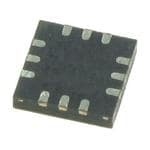
| 供应商器件封装 | 12-TQFN (1.6x2.2) |
| 其它名称 | PI3USB10MZKEXDKR |
| 功能 | USB 开关 |
| 包装 | Digi-Reel® |
| 安装类型 | 表面贴装 |
| 导通电阻 | 6.5 欧姆 |
| 封装/外壳 | 12-WFQFN 裸露焊盘 |
| 工作温度 | -40°C ~ 85°C |
| 标准包装 | 1 |
| 电压-电源,单/双 (±) | 2.7 V ~ 5 V |
| 电压源 | 单电源 |
| 电流-电源 | - |
| 电路 | 2 x 2:1 |


- 商务部:美国ITC正式对集成电路等产品启动337调查
- 曝三星4nm工艺存在良率问题 高通将骁龙8 Gen1或转产台积电
- 太阳诱电将投资9.5亿元在常州建新厂生产MLCC 预计2023年完工
- 英特尔发布欧洲新工厂建设计划 深化IDM 2.0 战略
- 台积电先进制程称霸业界 有大客户加持明年业绩稳了
- 达到5530亿美元!SIA预计今年全球半导体销售额将创下新高
- 英特尔拟将自动驾驶子公司Mobileye上市 估值或超500亿美元
- 三星加码芯片和SET,合并消费电子和移动部门,撤换高东真等 CEO
- 三星电子宣布重大人事变动 还合并消费电子和移动部门
- 海关总署:前11个月进口集成电路产品价值2.52万亿元 增长14.8%


PDF Datasheet 数据手册内容提取
PI3USB3102 USB3.0 and USB2.0 Combo Switch Features Description ÎÎ1:2 mux/demux for USB 3.0SS, 2.0HS, and 2.0FS signals Pericom Semiconductor’s PI3USB3102 USB3.0 and USB2.0 Com- ÎÎSwitches Tx, Rx, Dx, and USB_ID from USB3.0 connector bo Switch is a complete 1:2 switching solution for SuperSpeed USB 3.0 signals. PI3USB3102 provides differential high-speed ÎÎInsertion Loss for superspeed channels @ 2.5 GHz: -1.7dB lanes for the USB3.0 4.8 Gbps TX and RX lanes as well as a differ- ÎÎ-3dB Bandwidth for superspeed channels: 4.7GHz ential lane for 480 Mbps USB 2.0 signals and the USB_ID signal. ÎÎReturn loss for superspeed channels @ 2.5GHz: -16dB ÎÎLow Bit-to-Bit Skew, 7ps max (between '+' and '-' bits) PI3USB3102 can be used to connect two hosts to a single device ÎÎLow Crosstalk for superspeed channels: -25dB@5.0 Gbps or a single host to two devices. ÎÎLow Off Isolation for superspeed channels: -25dB@5.0 Gbps ÎÎVDD Operating Range: 3.3V +/-10% PI3USB3102 offers excellent signal integrity for high-speed sig- ÎÎESD Tolerance: 2kV HBM nals and low power dissipation. Insertion loss is 1.7 dB and return loss is -16 dB at 2.5 GHz. Power dissipation is 6.6 mW maximum. ÎÎLow channel-to-channel skew, 35ps max ÎÎPackaging (Pb-free & Green): à 32 TQFN (ZL) Application Routing of USB3.0 signals with low signal attenuation between source and sink. Block Diagram Tx+ Tx+A Tx- Tx-A Rx+ Rx+A Rx- Rx-A Tx+B Tx-B Rx+B Rx-B D+ D+A D- D-A USB_ID USB_ID A D+B D-B USB_ID B OE Logic SS SEL Control HS SEL 12-0264 1 11/09/12
PI3USB3102 USB3.0 and 2.0 Combo switch Pin Assignment (TQFN-32) Truth Table OE SS_SEL HS_SEL Function L E S_S +A -A DD ND LLooww LLooww HLoigwh PorPt oAr tf oAr aScSt,i vpeo frot rB a flol rc hHaSn annelds ID x x H T T V G Low High Low Port B for SS, port A for HS and ID 32 31 30 29 28 Low High High Port B active for all channels Tx+ 1 27 Rx+A High x x I/O's are hi-z and IC is power down Tx- 2 26 Rx-A VDD 3 25 Tx+B Rx+ 4 24 Tx-B Rx- 5 23 Rx+B GND D+ 6 22 Rx-B D- 7 21 GND USB_ID 8 20 VDD VDD 9 19 D+A SS_SEL 10 18 D-A OE 11 17 USB_IDA 2 3 4 5 6 1 1 1 1 1 D B B B D D D - + D V _I D D V B S U 12-0264 2 11/09/12
PI3USB3102 USB3.0 and 2.0 Combo switch Pin Description pin# pin Name Signal Type Description 1 Tx+ I/O positive differential USB3.0 Tx signal for COM port 2 Tx- I/O negative differential USB3.0 Tx signal for COM port 3 VDD Power 3.3V +/-10% power supply 4 Rx+ I/O positive differential USB3.0 Rx signal for COM port 5 Rx- I/O negative differential USB3.0 Rx signal for COM port 6 D+ I/O positive differential USB2.0 signal for COM port 7 D- I/O negative differential USB2.0 signal for COM port 8 USB_ID I/O USB_ID for COM port 9 VDD Power 3.3V +/-10% power supply switch logic control for SuperSpeed Path 10 SS_SEL I If HIGH, then path B is selected for SuperSpeed channels only If LOW, then path A is selected for SuperSpeed channels only Output enable. if OE is low, IC is enabled. If OE is high, then IC is power 11 OE I down and all I/Os are hi-z 12 VDD Power 3.3V +/-10% power supply 13 USB_IDB I/O USB_ID for port B 14 D-B I/O negative differential USB2.0 signal for port B 15 D+B I/O positive differential USB2.0 signal for port B 16 VDD Power 3.3V +/-10% power supply 17 USB_IDA I/O USB_ID for port A 18 D-A I/O negative differential USB2.0 signal for port A 19 D+A I/O positive differential USB2.0 signal for port A 20 VDD Power 3.3V +/-10% power supply 21 GND Ground Ground 22 Rx-B I/O negative differential USB3.0 Rx signal for port B 23 Rx+B I/O positive differential USB3.0 Rx signal for port B 24 Tx-B I/O negative differential USB3.0 Tx signal for port B 25 Tx+B I/O positive differential USB3.0 Tx signal for port B 26 Rx-A I/O negative differential USB3.0 Rx signal for port A 27 Rx+A I/O positive differential USB3.0 Rx signal for port A 28 GND Ground Ground 29 VDD Power 3.3V +/-10% power supply 30 Tx-A I/O negative differential USB3.0 Tx signal for port A 31 Tx+A I/O positive differential USB3.0 Tx signal for port A switch logic control for USB2.0 (D+/-) and USB_ID path 32 HS_SEL I If High, path B is selected If LOW, path A is selected 12-0264 3 11/09/12
PI3USB3102 USB3.0 and 2.0 Combo switch Maximum Ratings (Above which useful life may be impaired. For user guidelines, not tested.) Note: Stresses greater than those listed under MAXI- Storage Temperature ..........................................................–65°C to +150°C MUM RATINGS may cause permanent damage to the Supply Voltage to Ground Potential ....................................–0.5V to +4.2V device. This is a stress rating only and functional op- eration of the device at these or any other conditions DC Input Voltage .....................................................................–0.5V to VDD above those indicated in the operational sections of this DC Output Current .............................................................................120mA specification is not implied. Exposure to absolute maxi- Power Dissipation ...................................................................................0.5W mum rating conditions for extended periods may affect reliability. DC Electrical Characteristics for Switching over Operating Range (TA = –40°C to +85°C, VDD = 3.3V ±10%) Parameter Description Test Conditions(1) Min Typ(1) Max Units VIH Input HIGH Voltage Guaranteed HIGH level 1.5 VIL Input LOW Voltage Guaranteed LOW level 0.75 V VIK Clamp Diode Voltage, Dx VDD = Max., IIN = –18mA –0.8 –1.1 IIH Input HIGH Current VDD = Max., VIN = VDD ±5 IIL Input LOW Current VDD = Max., VIN = GND ±5 µA I/O leakage when part is off for D+, IOFF_HS/ID D- and USB_ID signals only VDD = 0V, VINPUT = 0V to 3.6V 20 On resistance between input to out- VDD = 3.3V, Vinput = 0V to 1V, RON_SS 10 13 Ohm put for SuperSpeed signals IINPUT = 20mA On resistance between input to out- VDD = 3.3V, Vinput = 0 to 3.3V, RON_FS 7 9 Ohm put for USB2.0 FS signals (D+/D-) IINPUT = 20mA On resistance between input to out- VDD = 3.3V, Vinput = -0.4V to RON_HS 4 6 Ohm put for USB2.0 HS signals (D+/D-) +0.4V, IINPUT = 20mA Input voltage tolerance on USB_ID USB_ID_I 5.5 V path USB_ID_O Output voltage on USB_ID path USB_ID input from 0V to 5.25V 3.6 V Power Supply Characteristics (TA = –40°C to +85°C) Parameter Description Test Conditions(1) Min Typ(1) Max Units ICC Quiescent Power Supply Current VDD = Max., VIN = GND or VDD 2 mA 12-0264 4 11/09/12
PI3USB3102 USB3.0 and 2.0 Combo switch Dynamic Electrical Characteristics over Operating Range (TA = -40º to +85ºC, VDD = 3.3V ±10%) Parameter Description Test Conditions Typ. Max Units See Fig. 1 for Measurement XTALK Crosstalk on SuperSpeed Channels f= 2.5 GHz -25dB Setup dB See Fig. 2 for Measurement OIRR OFF Isolation on SuperSpeed Channels f= 2.5 GHz -22dB Setup, Differential Insertion Loss on SuperSpeed ILOSS @5.0Gbps (see figure 3) -1.7 dB Channels Differential Return Loss on SuperSpeed Rloss @ 2.5GHz -16 dB channels Bandwidth -3dB for SuperSpeed path BW_SS See figure 3 4.7 GHz (Tx±/ Rx±) BW_HS -3dB BW for USB high speed path (D+/-) See figure 3 1.5 GHz time it takes to switch from port A to port Tsw a-b 1 us B time it takes to switch from port B to port Tsw b-a 1 us A Tstartup Vdd valid to channel enable 10 us Enabling output by changing OE from Twakeup 10 us low to High 1. For Max. or Min. conditions, use appropriate value specified under Electrical Characteristics for the applicable device type. 2. Typical values are at VDD = 3.3V, TA = 25°C ambient and maximum loading. Switching Characteristics (TA= -40º to +85ºC, VDD = 3.3V±10%) Parameter Description Min. Typ. Max. Units Tpd Propagation delay (input pin to output pin) 80 ps tb-b Bit-to-bit skew within the same differential pair 5 ps tch-ch Channel-to-channel skew 35 ps 12-0264 5 11/09/12
PI3USB3102 USB3.0 and 2.0 Combo switch 50 + + BALANCED PORT1 – – 50 + + 50 BALANCED PORT2 – – 50 DUT Fig 1. Crosstalk Setup 50 + + BALANCED PORT1 – – 50 + BALANCED – PORT2 DUT Fig 2. Off-isolation setup + + BALANCED BALANCED PORT1 – – PORT2 DUT Fig 3. Differential Insertion Loss set up 12-0264 6 11/09/12
PI3USB3102 USB3.0 and 2.0 Combo switch -20.0 -30.0 -40.0 -50.0 -60.0 B) d k ( stal-70.0 s o Cr -80.0 -90.0 -100.0 1.00E+07 1.00E+08 1.00E+09 1.00E+10 Frequency (Hz) Fig 4. Xtalk for SuperSpeed channels (Tx/Rx) 12-0264 7 11/09/12
PI3USB3102 USB3.0 and 2.0 Combo switch -0.0 -10.0 -20.0 -30.0 B)-40.0 d n ( o ati ol-50.0 s Off I -60.0 -70.0 -80.0 1.00E+07 1.00E+08 1.00E+09 1.00E+10 Frequency (Hz) Fig 5. Off Isolation for SuperSpeed channels (Tx/Rx). Red is for path B and Blue is for path A 12-0264 8 11/09/12
PI3USB3102 USB3.0 and 2.0 Combo switch -0.0 -1.0 -2.0 B) d s ( -3.0 s o L n o erti s n I -4.0 -5.0 -6.0 1.00E+07 1.00E+08 1.00E+09 1.00E+10 Frequency (Hz) Fig 6. Insertion Loss for SuperSpeed channels (Tx/Rx). Red is for path B and Blue is for path A 12-0264 9 11/09/12
PI3USB3102 USB3.0 and 2.0 Combo switch Test Circuit for Electrical Characteristics(1-5) 2 * Vdd VDD 200-ohm Pulse VIN VOUT D.U.T Generator 4pF RT CL 200-ohm Notes: 1. CL = Load capacitance: includes jig and probe capacitance. 2. RT = Termination resistance: should be equal to ZOUT of the Pulse Generator 3. Output 1 is for an output with internal conditions such that the output is low except when disabled by the output control. 4. Output 2 is for an output with internal conditions such that the output is high except when disabled by the output control. 5. All input impulses are supplied by generators having the following characteristics: PRR ≤ MHz, ZO = 50Ω, tR ≤ 2.5ns, tF ≤ 2.5ns. 6. The outputs are measured one at a time with one transition per measurement. Switching Waveforms SEL VDD 50% 50% 0V tPZL Output 1 tPLZ VOH 10% VOL tPZH tPHZ VOH 90% Output 2 VOL Voltage Waveforms Enable and Disable Times Switch Positions Test Switch tPLZ, tPZL (output on B-side) 2 * Vdd tPHZ, tPZH (output on B-side) GND Prop Delay Open Test Circuit for Dynamic Electrical Characteristics Agilent PNA-L Network Analyzer Balanced port 1 Balanced port 2 DUT 12-0264 10 11/09/12
PI3USB3102 USB3.0 and 2.0 Combo switch Packaging Mechanical: 32-Contact TQFN (ZL) 1 DATE: 10/09/09 DESCRIPTION: 32-contact, Thin Fine Pitch Quad Flat No-Lead (TQFN) PACKAGE CODE: ZL (ZL32) DOCUMENT CONTROL #: PD-2044 REVISION: A 09-0125 Note: For latest package info, please check: http://www.pericom.com/products/packaging/mechanicals.php Ordering Information Ordering Code Package Code Package Description PI3USB3102ZLE ZL Pb-free & Green, 32-contact TQFN, Copper Wire PI3USB3102ZLE+DA ZL Pb-free & Green, 32-contact TQFN, Gold Wire Notes: • Thermal characteristics can be found on the company web site at www.pericom.com/packaging/ • "E" denotes Pb-free and Green • Adding an "X" at the end of the ordering code denotes tape and reel packaging 12-0264 11 11/09/12
Mouser Electronics Authorized Distributor Click to View Pricing, Inventory, Delivery & Lifecycle Information: D iodes Incorporated: PI3USB102ZMEX PI2USB4122ZHEX