ICGOO在线商城 > 集成电路(IC) > 接口 - 模拟开关 - 专用 > MAX4888BGTI+

 Datasheet下载
- 型号: MAX4888BGTI+
- 制造商: Maxim
- 库位|库存: xxxx|xxxx
- 要求:
| 数量阶梯 | 香港交货 | 国内含税 |
| +xxxx | $xxxx | ¥xxxx |
查看当月历史价格
查看今年历史价格
MAX4888BGTI+产品简介:
ICGOO电子元器件商城为您提供MAX4888BGTI+由Maxim设计生产,在icgoo商城现货销售,并且可以通过原厂、代理商等渠道进行代购。 MAX4888BGTI+价格参考。MaximMAX4888BGTI+封装/规格:接口 - 模拟开关 - 专用, PCI Express® 开关 IC 2 通道 28-TQFN(3.5x5.5)。您可以下载MAX4888BGTI+参考资料、Datasheet数据手册功能说明书,资料中有MAX4888BGTI+ 详细功能的应用电路图电压和使用方法及教程。
MAX4888BGTI+ 是由 Maxim Integrated 生产的一款专用模拟开关,属于接口 - 模拟开关 - 专用分类。该器件主要用于需要高速、低功耗和高可靠性的信号切换应用中,特别适用于通信、数据采集、测试测量以及工业控制系统等领域。

 应用场景:

1. 通信设备:
   - MAX4888BGTI+ 可用于通信系统中的信号路径选择,例如在多通道接收器或发射器中,实现不同信道之间的快速切换。其低电容和低导通电阻特性确保了信号完整性,适用于高速数据传输。

2. 数据采集系统:
   - 在数据采集系统中,MAX4888BGTI+ 可以用于传感器信号的多路复用,将多个传感器输入信号切换到一个ADC(模数转换器)进行处理。它的低泄漏电流和高线性度保证了信号的准确性,适合精密测量应用。

3. 测试与测量仪器:
   - 测试测量设备如示波器、信号发生器等,需要在不同信号源之间进行快速切换。MAX4888BGTI+ 的快速开关时间和低插入损耗使其成为这些应用的理想选择,能够提高测试效率和精度。

4. 工业控制系统:
   - 在工业自动化系统中,MAX4888BGTI+ 可用于控制信号的切换,确保不同设备之间的通信顺畅。其高可靠性设计能够在恶劣环境下长期稳定工作,适用于工厂自动化、过程控制等领域。

5. 医疗设备:
   - 医疗设备如心电图机、超声波设备等需要对多个生理信号进行实时监测和切换。MAX4888BGTI+ 的低噪声和高稳定性特性有助于提高设备的性能和安全性。

6. 音频处理:
   - 在音频设备中,MAX4888BGTI+ 可用于音频信号的切换,确保不同音源之间的无缝切换,同时保持高质量的音频输出。

总之,MAX4888BGTI+ 凭借其优异的电气性能和可靠性,广泛应用于各种需要高性能信号切换的场合,特别是在对速度、精度和可靠性要求较高的领域。
| 参数 | 数值 |
| 产品目录 | 集成电路 (IC) |
| 描述 | IC SWITCH QUAD SPDT 28TQFN |
| 产品分类 | |
| 品牌 | Maxim Integrated |
| 数据手册 | |
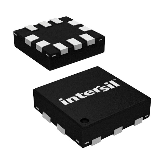
| 产品图片 |
|
| 产品型号 | MAX4888BGTI+ |
| rohs | 无铅 / 符合限制有害物质指令(RoHS)规范要求 |
| 产品系列 | - |
| 产品培训模块 | http://www.digikey.cn/PTM/IndividualPTM.page?site=cn&lang=zhs&ptm=30301 |
| 供应商器件封装 | 28-TQFN-EP(3.5x5.5) |
| 功能 | |
| 包装 | 管件 |
| 安装类型 | 表面贴装 |
| 导通电阻 | 8 欧姆 |
| 封装/外壳 | 28-WFQFN 裸露焊盘 |
| 工作温度 | -40°C ~ 85°C |
| 应用说明 | |
| 标准包装 | 1 |
| 电压-电源,单/双 (±) | 3 V ~ 3.6 V |
| 电压源 | 单电源 |
| 电流-电源 | 1mA |
| 电路 | 2 x DPDT |


- 商务部:美国ITC正式对集成电路等产品启动337调查
- 曝三星4nm工艺存在良率问题 高通将骁龙8 Gen1或转产台积电
- 太阳诱电将投资9.5亿元在常州建新厂生产MLCC 预计2023年完工
- 英特尔发布欧洲新工厂建设计划 深化IDM 2.0 战略
- 台积电先进制程称霸业界 有大客户加持明年业绩稳了
- 达到5530亿美元!SIA预计今年全球半导体销售额将创下新高
- 英特尔拟将自动驾驶子公司Mobileye上市 估值或超500亿美元
- 三星加码芯片和SET,合并消费电子和移动部门,撤换高东真等 CEO
- 三星电子宣布重大人事变动 还合并消费电子和移动部门
- 海关总署:前11个月进口集成电路产品价值2.52万亿元 增长14.8%


PDF Datasheet 数据手册内容提取
19-5706; Rev 0; 12/10 EVAALVUAAILTAIOBNL EKIT Up to 8.0Gbps Dual Passive Switches General Description Features M The MAX4888B/MAX4888C dual double-pole/double- S Single +3.3V Power-Supply Voltage A throw (2 x DPDT), high-speed passive switches are S Supports PCIe Gen I, Gen II, and Gen III Data X ideal for switching two half-lanes of PCI ExpressM (PCIe) Rates 4 data between two possible destinations. These devices S Supports Up To and Including 6.0Gbps SAS/SATA 8 feature a dual digital control input to switch signal paths. Signals 8 The MAX4888C is intended for use in systems where both the input and output are capacitively coupled (e.g., S Supports Other High-Speed Interfaces (e.g., XAUI) 8 SAS, SATA, XAUI, and PCIe) and provides a 10FA (typ) B S Superior Bandwidth Return Loss source current and a 60kI (typ) internal biasing resistor / S Small, 3.5mm x 5.5mm, 28-Pin TQFN Package M to GND at the AOUT_ and BOUT_ pins. The devices are fully specified to operate from a single A Ordering Information +3.3V (typ) power supply. Both devices are available X in an industry-standard 3.5mm x 5.5mm, 28-pin TQFN PART TEMP RANGE PIN-PACKAGE 4 package. They operate over the -40NC to +85NC extend- MAX4888BETI+ -40NC to +85NC 28 TQFN-EP* 8 ed temperature range. MAX4888CETI+ -40NC to +85NC 28 TQFN-EP* 8 Applications +Denotes a lead(Pb)-free/RoHS-compliant package. 8 *EP = Exposed pad. C Desktop PCs Notebook PCs Servers Typical Operating Circuit CONNECTION SELECT VCC VCC AOUTA+ SEL SEL AOUTA+ AOUTA- AOUTA- PCIe HOST PCIe DEVICE BOUTA+ SELB SELB BOUTA+ BOUTA- BOUTA- AIN+ AIN+ MAX4888C AIN- AIN- MAX4888C BIN+ BIN+ AOUTB+ BIN- BIN- AOUTB+ AOUTB- AOUTB- SAS HOST SAS DEVICE BOUTB+ BOUTB+ BOUTB- BOUTB- GND GND NOTE: CAPACITIVE COUPLING WAS OMITTED TO SIMPLIFY ILLUSTRATION. PCI Express is a registered trademark of PCI-SIG Corp. _______________________________________________________________ Maxim Integrated Products 1 For pricing, delivery, and ordering information, please contact Maxim Direct at 1-888-629-4642, or visit Maxim’s website at www.maxim-ic.com.
Up to 8.0Gbps Dual Passive Switches C ABSOLUTE MAXIMUM RATINGS 8 (All voltages referenced to GND, unless otherwise noted.) Continuous Current (SEL, SELB) ....................................Q10mA 8 VCC ..........................................................................-0.3V to +4V Peak Current (SEL, SELB) 8 SEL, SELB, AIN+, AIN-, BIN+, BIN-, AOUTA+, (pulsed at 1ms, 10% duty cycle) ................................Q10mA 4 AOUTA-, AOUTB+, AOUTB-, BOUTA+, Continuous Power Dissipation (TA = +70NC) BOUTA-, BOUTB+, BOUTB- (Note 1) ..-0.3V to (VCC + 0.3V) TQFN (derate 28.6mW/NC above +70NC)..................2286mW X Continuous Current (AIN_ to AOUTA_/AOUTB_, Operating Temperature Range ..........................-40NC to +85NC A BIN_ to BOUTA_/BOUTB_) ..........................................Q15mA Junction Temperature .....................................................+150NC Peak Current (AIN_ to AOUTA_/AOUTB_, Storage Temperature Range ............................-65NC to +150NC M BIN_ to BOUTA_/BOUTB_) Lead Temperature (soldering, 10s) ................................+300NC / (pulsed at 1ms, 10% duty cycle) ................................Q70mA Soldering Temperature (reflow) ......................................+260NC B 8 Note 1: Signals on SEL, SELB, AIN_, BIN _, AOUTA_, AOUTB_, BOUTA_, and BOUTB_ exceeding VCC or GND are clamped by internal diodes. Limit forward-diode current to maximum current rating. 8 8 PACKAGE THERMAL CHARACTERISTICS (Note 2) 4 TQFN X Junction-to-Ambient Thermal Resistance (qJA) ..........35°C/W A Junction-to-Case Thermal Resistance (qJC) .................2°C/W M Note 2: Package thermal resistances were obtained using the method described in JEDEC specification JESD51-7, using a four- layer board. For detailed information on package thermal considerations, refer to www.maxim-ic.com/thermal-tutorial. Stresses beyond those listed under “Absolute Maximum Ratings” may cause permanent damage to the device. These are stress ratings only, and functional operation of the device at these or any other conditions beyond those indicated in the operational sections of the specifications is not implied. Exposure to absolute maximum rating conditions for extended periods may affect device reliability. ELECTRICAL CHARACTERISTICS (VCC = 3.3V Q10%, TA = -40NC to +85NC, unless otherwise noted. Typical values are at VCC = 3.3V, TA = +25NC, unless otherwise noted.) (Note 3) PARAMETER SYMBOL CONDITIONS MIN TYP MAX UNITS DC PERFORMANCE AIN_, BIN_, AOUTA_, BOUTA_, AOUTB_, VCC - Analog-Signal Range VINPUT -0.3 V BOUTB_ 1.8 VCC = +3.0V, IAIN_ = IBIN_ = 15mA, On-Resistance RON 6.4 8.4 I V_OUTA_ = V_OUTB_ = 0V, 1.2V On-Resistance Match VCC = +3.0V, IAIN_ = IBIN_ = 15mA, DRON 0.2 1.5 I Between Channels V_OUTA_ = V_OUTB_ = 0V (Note 4) VCC = +3.0V, IAIN_ = IBIN_ = 15mA, On-Resistance Flatness RFLAT(ON) 0.3 1 I V_OUTA_ = V_OUTB_ = 0V, 1.2V (Note 5) VCC = +3.6V, VAIN_ = VBIN_ = 0V, 1.2V; _OUTA_ or _OUTB_ I_OUTA_(OFF), V_OUTA_ or V_OUTB_ = 1.2V, 0V -1 +1 FA Off-Leakage Current I_OUTB_(OFF) (MAX4888B) VCC = +3.6V , VAIN_ = VBIN_ = 0V, 1.2V; IAIN_(ON), AIN_, BIN_ On-Leakage Current V_OUTA_ or V_OUTB_ = VAIN_ = VBIN_ or -1 +1 FA IBIN_(ON) unconnected (MAX4888B) All other ports are unconnected Output Short-Circuit Current 5 15 FA (MAX4888C) All other ports are unconnected Output Open-Circuit Voltage 0.2 0.6 0.9 V (MAX4888C) 2
Up to 8.0Gbps Dual Passive Switches ELECTRICAL CHARACTERISTICS (continued) M (VCC = 3.3V Q10%, TA = -40NC to +85NC, unless otherwise noted. Typical values are at VCC = 3.3V, TA = +25NC, unless otherwise A noted.) (Note 3) X PARAMETER SYMBOL CONDITIONS MIN TYP MAX UNITS 4 AC PERFORMANCE 8 Switch Turn-On Time tON_SEL ZS = ZL = 50I 65 ns 8 Switch Turn-Off Time tOFF_SEL ZS = ZL = 50I, Figure 1, measured at 7 ns 8 500MHz B ZS = ZL = 50I, Figure 2, measured at Propagation Delay tPD 43 ps / 500MHz M Output Skew Between Pairs tSK1 ZS = ZL = 50I, Figure 2, measured at 8 ps A 500MHz X Output Skew Between Same tSK2 ZS = ZL = 50I, Figure2 10 ps 4 Pair 8 0Hz < f P 2.8GHz -14 8 2.8GHz < f P 5.0GHz -8 Differential Return Loss (Note 6) SDD11 dB 8 5.0GHz < f P 8.0GHz -5 C f > 8.0GHz -1 Differential Insertion Loss SDD21 Table 1 dB Bandwidth SDD12/SDD21 8 GHz 0Hz < f P 2.5GHz -30 2.5GHz < f P 5.0GHz -25 Differential Crosstalk (Note 6) SDDCTK dB 5.0GHz < f P 8.0GHz -35 f > 8.0GHz -35 0Hz < f P 2.5GHz -15 2.5GHz < f P 5.0GHz -12 Differential Off-Isolation (Note 6) SDD21_OFF dB 5.0GHz < f P 8.0GHz -12 f > 8.0GHz -12 CONTROL INPUT Input Logic-High VIH 1.4 V Input Logic-Low VIL 0.6 V Input Logic Hysteresis VHYST 130 mV POWER SUPPLY Power-Supply Range VCC 3.0 3.6 V VCC Supply Current ICC 1 mA Note 3: All units are 100% production tested at TA = +85NC. Limits over the operating temperature range are guaranteed by design and characterization and are not production tested. Note 4: DRON = RON(MAX) - RON(MIN). Note 5: Flatness is defined as the difference between the maximum and minimum value of on-resistance as measured over the specified analog-signal range. Note 6: Guaranteed by design; not production tested. 3
Up to 8.0Gbps Dual Passive Switches C Test Circuits/Timing Diagrams 8 8 8 SOURCE LOAD 4 MAX4888B X MAX4888C A ZS VOUT M Σ ZL / SEL B 8 8 8 4 X SEL 50% 50% A M 90% VOUT 10% tON_SEL tOFF_SEL THE FREQUENCY OF THE SIGNAL SHOULD BE ABOVE THE HIGHPASS FILTER CORNER OF THE COUPLING CAPACITORS. Figure 1. Switching Time Table 1. Insertion Loss Mask FREQUENCY RANGE (GHz) MAXIMUM INSERTION LOSS (dB) 0 to 2.5 1/3 x fGHZ + 17/30 2.5 to 5 2/5 x fGHZ - 2/5 5 to 8 18/5 x fGHZ - 4/15 Greater than 8 2 x fGHZ - 12 4
Up to 8.0Gbps Dual Passive Switches Test Circuits/Timing Diagrams (continued) M A X SOURCE LOAD 4 MAX4888B MAX4888C 8 ZS VOUTp 8 8 VS+ Σ ZL B ZS VOUTn / M VS- Σ ZL SEL A X ZS CALIBRATION VCALp 4 8 VSC+ Σ ZL ZS TRACES VCALn 8 8 VSC- Σ ZL C VCALp - VCALn 50% 50% VOUTp - VOUTn 50% 50% tPDr tPDf tPD = max (tPDr, tPDf) VOUTp VCM VCM VOUTn VCM VCM tSKEW = max (tSK1, tSK2) tSK1 tSK2 AFTER ELIMINATING SOURCE AND CABLE SKEWS. Figure 2. Propagation Delay and Output Skew 5
Up to 8.0Gbps Dual Passive Switches C Typical Operating Characteristics 8 (VCC = 3.3V, TA = +25NC, unless otherwise noted.) 8 8 ON-RESISTANCE vs. V_IN_ ON-RESISTANCE vs. V_IN_ SUPPLY CURRENT vs. TEMPERATURE 4 MAX 778...050 VCC = 3.0V MAX4888B/C toc01 1890 TA = +85°C MAX4888B/C toc02 µA) 330500 VCC = 3.M6VAX4888B MAX4888C MAX4888B/C toc03 88B/ R ()ΩON 566...505 VCC = 3.3V VCC = 3.6V R ()ΩON 567 TA = +25°C SUPPLY CURRENT ( 220500 VVVVCCCCCCCC ==== 3333....3063VVVV 8 5.0 4 TA = -40°C 150 VCC = 3.0V 4.5 3 4 4.0 2 100 X 0 0.3 0.6 0.9 1.2 1.5 1.8 0 0.3 0.6 0.9 1.2 1.5 -40 -15 10 35 60 85 A V_IN_ (V) V_IN_ (V) TEMPERATURE (°C) M LOGIC THRESHOLD TURN-ON/OFF TIME DIFFERENTIAL RETURN LOSS vs. SUPPLY VOLTAGE vs. SUPPLY VOLTAGE vs. FREQUENCY RESHOLD (V) 1111....2345 VIH VIL MAX4888B/C toc04 OFF TIME (ns) 1567890000000 tON_SEL MAX4888B/C toc05 RETURN LOSS (dB) ----432100000 MASK MAX4888B/C toc06 LOGIC TH 11..01 TURN-ON/ 3400 FERENTIAL --6500 20 tOFF_SEL DIF 0.9 -70 10 MAX4888B MAX4888C 0.8 0 -80 3.0 3.1 3.2 3.3 3.4 3.5 3.6 3.0 3.1 3.2 3.3 3.4 3.5 3.6 0 2 4 6 8 10 VCC (V) VCC (V) FREQUENCY (GHz) DIFFERENTIAL INSERTION LOSS DIFFERENTIAL OFF-ISOLATION DIFFERENTIAL CROSSTALK vs. FREQUENCY vs. FREQUENCY vs. FREQUENCY 0 0 0 DIFFERENTIAL INSERTION LOSS (dB) ----1111----86426420 MASK MAX4888B/C toc07 DIFFERENTIAL OFF-ISOLATION (dB) ------654321000000 MAX4888B/C toc08 DIFFERENTIAL CROSSTALK (dB) --------8765432100000000 MAX4888B/C toc09 -70 -18 -90 MAX4888B MAX4888C -20 -80 -100 0 2 4 6 8 10 0 2 4 6 8 10 0 2 4 6 8 10 FREQUENCY (GHz) FREQUENCY (GHz) FREQUENCY (GHz) 6
Up to 8.0Gbps Dual Passive Switches Pin Configuration M A TOP VIEW X A+ A- A+ A- SEL GND AOUT AOUT GND VCC BOUT BOUT GND SELB 4 8 24 23 22 21 20 19 18 17 16 15 8 VCC 25 14 VCC 8 GND 26 13 GND MAX4888B B VCC 27 MAX4888C 12 VCC / GND 28 + *EP 11 GND M 1 2 3 4 5 6 7 8 9 10 A GND AIN+ AIN- UTB+ UTB- BIN+ BIN- UTB+ UTB- GND X O O O O A A B B 4 TQFN 8 *CONNECT EXPOSED PAD TO GND. 8 8 C Pin Description PIN NAME FUNCTION 1, 10, 11, 13, 16, GND Ground 20, 23, 26, 28 2 AIN+ Analog Switch 1, Common Positive Terminal 3 AIN- Analog Switch 1, Common Negative Terminal 4 AOUTB+ Analog Switch 1, Normally Open Positive Terminal 5 AOUTB- Analog Switch 1, Normally Open Negative Terminal 6 BIN+ Analog Switch 2, Common Positive Terminal 7 BIN- Analog Switch 2, Common Negative Terminal 8 BOUTB+ Analog Switch 2, Normally Open Positive Terminal 9 BOUTB- Analog Switch 2, Normally Open Negative Terminal 12, 14, Positive Supply-Voltage Input. Connect VCC to a 3.0V to 3.6V supply voltage. Bypass VCC to GND with 19, 25, VCC a 0.1FF ceramic capacitor placed as close as possible to the device. See the Board Layout section. 27 Control Signal Input. SELB has a 70kI (typ) pullup resistor to VCC. If SELB is not in use, leave 15 SELB unconnected. 17 BOUTA- Analog Switch 2, Normally Closed Negative Terminal 18 BOUTA+ Analog Switch 2, Normally Closed Positive Terminal 21 AOUTA- Analog Switch 1, Normally Closed Negative Terminal 22 AOUTA+ Analog Switch 1, Normally Closed Positive Terminal 24 SEL Control Signal Input. SEL has a 70kI (typ) pulldown resistor to GND. — EP Exposed Pad. Connect EP to GND. 7
Up to 8.0Gbps Dual Passive Switches C Functional Diagram/Truth Table 8 8 VCC VCC 8 4 X MAX4888B MAX4888C A AIN+ AOUTA+ AIN+ AOUTA+ M / B AIN- AOUTA- AIN- AOUTA- 8 8 8 4 X AOUTB+ AOUTB+ A M AOUTB- AOUTB- BIN+ BOUTA+ BIN+ BOUTA+ BIN- BOUTA- BIN- BOUTA- BOUTB+ BOUTB+ BOUTB- BOUTB- VCC VCC SELB AIN_, BIN_ AIN_, BIN_ SELB SEL CONTROL SEL SELB TO AOUTA_, TO AOUTB_, SEL CONTROL BOUTA_ BOUTB_ 0 (DEFAULT) 0 OFF ON 1 0 OFF ON 0 (DEFAULT) 1 (DEFAULT) ON OFF GND GND 1 1 (DEFAULT) OFF ON 8
Up to 8.0Gbps Dual Passive Switches Detailed Description Applications Information M The MAX4888B high-speed passive switch routes high- High-Speed Switching A speed differential signals such as PCIe, SAS, SATA, The devices’ primary applications are aimed at sharing X and XAUI from one source to two possible destina- resources. For example, a single lane of PCIe or SAS 4 tions or vice versa. The MAX4888B is ideal for routing can be shared between a single host and two devices. 8 PCIe signals to change the system configuration. The This could be used for redundancy or to share resources 8 MAX4888C features a 10FA (typ) source current and such as a physical lane or route a lane between one host a 60kI (typ) internal biasing resistor to GND at the and two devices or two hosts and one device. 8 AOUTA_, BOUTA_, AOUTB_, and BOUTB_ terminals. B The MAX4888C is ideal for circuits that are capacitively Board Layout / coupled at both the output and input. These devices are High-speed switches require proper layout and design M protocol independent and can be used to switch two dif- procedures for optimum performance. Keep controlled A ferent protocol signals over the same physical lane. They impedance PCB traces as short as possible or follow feature dual digital control inputs (SEL, SELB) to switch impedance layouts per the PCIe specification. Ensure X signal paths. SEL has a 70kI (typ) pulldown resistor to that power-supply bypass capacitors are placed as 4 GND and SELB has a 70kI (typ) pullup resistor to VCC. close as possible to the device. Multiple bypass capaci- 8 tors are recommended. Connect all grounds and the These devices are fully specified to operate from a single 8 exposed pad to a large ground plane. 3.0V to 3.6V power supply. 8 Chip Information C Digital Control Input (SEL, SELB) The devices provide dual digital control inputs (SEL, PROCESS: CMOS SELB) to select the signal path between the AIN_, BIN_ and AOUTA_, BOUTA_ or AOUTB_, BOUTB_ chan- Package Information nels. In most cases SEL is chosen and SELB is uncon- For the latest package outline information and land patterns, nected. The truth table for the devices is depicted in the go to www.maxim-ic.com/packages. Note that a “+”, “#”, or Functional Diagram/Truth Table. SEL has a 70kI (typ) “-” in the package code indicates RoHS status only. Package pulldown resistor to GND and SELB has a 70kI (typ) drawings may show a different suffix character, but the drawing pullup resistor to VCC. pertains to the package regardless of RoHS status. Analog-Signal Levels PACKAGE PACKAGE OUTLINE LAND The devices accept signals from -0.3V to (VCC - 1.8V). TYPE CODE NO. PATTERN NO. Signals on the AIN+ and BIN+ channels are routed to 28 TQFN-EP T283555+1 21-0184 90-0123 either the AOUTA+, BOUTA+ or AOUTB+, BOUTB+ channels. Signals on the AIN- and BIN- channels are rout- ed to either the AOUTA-, BOUTA- or AOUTB-, BOUTB- channels. The devices are bidirectional switches, allow- ing AIN_, BIN_ and AOUTA_, BOUTA_, AOUTB_, and BOUTB_ to be used as either inputs or outputs. 9
Up to 8.0Gbps Dual Passive Switches C Revision History 8 8 REVISION REVISION PAGES DESCRIPTION NUMBER DATE CHANGED 8 4 0 12/10 Initial release — X A M / B 8 8 8 4 X A M Maxim cannot assume responsibility for use of any circuitry other than circuitry entirely embodied in a Maxim product. No circuit patent licenses are implied. Maxim reserves the right to change the circuitry and specifications without notice at any time. 10 Maxim Integrated Products, 120 San Gabriel Drive, Sunnyvale, CA 94086 408-737-7600 © 2010 Maxim Integrated Products Maxim is a registered trademark of Maxim Integrated Products, Inc.