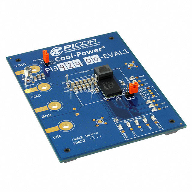
ICGOO在线商城 > 开发板,套件,编程器 > 评估板 - DC/DC 与 AC/DC(离线)SMPS > PI3424-00-EVAL1
 Datasheet下载
- 型号: PI3424-00-EVAL1
- 制造商: Vicor
- 库位|库存: xxxx|xxxx
- 要求:
| 数量阶梯 | 香港交货 | 国内含税 |
| +xxxx | $xxxx | ¥xxxx |
查看当月历史价格
查看今年历史价格
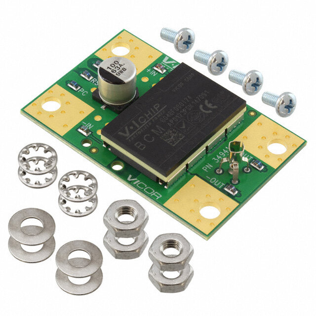
PI3424-00-EVAL1产品简介:
ICGOO电子元器件商城为您提供PI3424-00-EVAL1由Vicor设计生产,在icgoo商城现货销售,并且可以通过原厂、代理商等渠道进行代购。 PI3424-00-EVAL1价格参考。VicorPI3424-00-EVAL1封装/规格:评估板 - DC/DC 与 AC/DC(离线)SMPS, PI3424-00 Cool-Power® DC/DC,步降 1,非隔离 Outputs Evaluation Board。您可以下载PI3424-00-EVAL1参考资料、Datasheet数据手册功能说明书,资料中有PI3424-00-EVAL1 详细功能的应用电路图电压和使用方法及教程。
PI3424-00-EVAL1是Vicor Corporation推出的一款评估板,专为PI3424 DC/DC转换器模块设计,属于DC/DC与AC/DC(离线)SMPS类电源管理产品。该评估板主要用于帮助工程师快速评估和验证PI3424模块在实际应用中的性能表现。

其主要应用场景包括高性能计算、数据中心电源架构、工业自动化设备、通信基础设施(如5G基站和网络交换设备)以及嵌入式系统等。这些领域对电源效率、功率密度和热管理有较高要求,而PI3424-00-EVAL1支持高效率、高密度的电源转换,具备宽输入电压范围和稳定输出特性,便于用户测试模块在不同负载和输入条件下的动态响应、热性能及EMI表现。

通过该评估板,用户无需复杂设计即可搭建测试环境,加快产品开发周期。同时,它支持多种并联与级联配置,适用于需要多路供电或冗余电源系统的场景。整体上,PI3424-00-EVAL1为研发人员提供了便捷、可靠的平台,用于优化电源系统设计,提升系统能效与可靠性。
| 参数 | 数值 |
| 产品目录 | 编程器,开发系统 |
| 描述 | PICOR COOL-POWER EVAL PI3424-00 |
| 产品分类 | |
| 品牌 | Vicor Corporation |
| 数据手册 | |
| 产品图片 |
|
| 产品型号 | PI3424-00-EVAL1 |
| rohs | 无铅 / 符合限制有害物质指令(RoHS)规范要求 |
| 产品系列 | Picor® Cool-Power® |
| 主要用途 | DC/DC,步降 |
| 使用的IC/零件 | PI3424-00 |
| 其它名称 | 1102-1639 |
| 功率-输出 | - |
| 所含物品 | 板 |
| 板类型 | 完全填充 |
| 标准包装 | 1 |
| 电压-输入 | 8 V ~ 18 V |
| 电压-输出 | 5V |
| 电流-输出 | 15A |
| 稳压器拓扑 | 降压 |
| 输出和类型 | 1,非隔离 |
| 频率-开关 | 750kHz |


- 商务部:美国ITC正式对集成电路等产品启动337调查
- 曝三星4nm工艺存在良率问题 高通将骁龙8 Gen1或转产台积电
- 太阳诱电将投资9.5亿元在常州建新厂生产MLCC 预计2023年完工
- 英特尔发布欧洲新工厂建设计划 深化IDM 2.0 战略
- 台积电先进制程称霸业界 有大客户加持明年业绩稳了
- 达到5530亿美元!SIA预计今年全球半导体销售额将创下新高
- 英特尔拟将自动驾驶子公司Mobileye上市 估值或超500亿美元
- 三星加码芯片和SET,合并消费电子和移动部门,撤换高东真等 CEO
- 三星电子宣布重大人事变动 还合并消费电子和移动部门
- 海关总署:前11个月进口集成电路产品价值2.52万亿元 增长14.8%


PDF Datasheet 数据手册内容提取
ZVS Regulators PI34xx-00 8 – 18V , 15A ZVS Buck Regulator IN Product Description Features & Benefits The PI34xx-00 is a family of high-efficiency DC-DC ZVS Buck • High-efficiency ZVS Buck topology regulators integrating the controller, power switches and support • Input voltage range of 8 – 18V components within a high-density System-in-Package (SiP). • Very fast transient response The PI34xx-00 is designed to achieve optimum efficiency at low input voltage ranges (8 – 18V). The utilization of zero-current soft • Power-up into pre-biased load turn-on provided by the high-performance ZVS topology within the PI34xx-00 series increases point-of-load performance, providing • High-accuracy pre-trimmed output voltage best in class power efficiency with high throughput power. • User adjustable soft start & tracking The PI34xx-00 requires only an external inductor and minimal • Parallel capable with single-wire current sharing capacitors to form a complete DC-DC switching-mode buck regulator. • Input over/undervoltage lockout (OVLO/UVLO) • Output overvoltage protection (OVP) Output Voltage Device I Max • Overtemperature Protection (OTP) OUT Set Range • Fast and slow current limits PI3420-00-LGIZ 1.0V 1.0 – 1.4V 15A • –40 to 125°C operating range (T ) INT PI3421-00-LGIZ 1.8V 1.4 – 2.0V 15A PI3422-00-LGIZ 2.5V 2.0 – 3.1V 15A Applications PI3423-00-LGIZ 3.3V 2.3 – 4.1V 15A • High-Efficiency Systems PI3424-00-LGIZ 5.0V 3.3 – 6.5V 15A • Computing, Communications, Industrial, The ZVS architecture enables high-frequency operation while Automotive Equipment minimizing switching losses and maximizing efficiency. The high-switching-frequency operation reduces the size of the external Package Information filtering components, improves power density, and enables very fast dynamic response to line and load transients. • 10 x 14 x 2.6mm LGA SiP The ZVS architecture enables operation up to 750kHz while minimizing switching losses and the use of variable frequency extends high efficiency over a very wide dynamic range. The PI34xx-00 series has a minimum on time of 20ns which enables large step-down conversion ratios. Note: Product images may not highlight current product markings. ZVS Regulators Rev 1.5 Page 1 of 31 02/2020
PI34xx-00 Contents Order Information 3 Application Description 24 Thermal, Storage and Handling Information 3 Output Voltage Trim 24 Absolute Maximum Ratings 3 Soft-Start Adjust and Tracking 25 Functional Block Diagram 4 Inductor Pairing 26 Pin Description 5 Thermal De-Rating 26 Package Pinout 6 Filter Considerations 26 PI3420-00-LGIZ (1.0V ) Electrical Characteristics 7 Layout Guidelines 27 OUT PI3421-00-LGIZ (1.8V ) Electrical Characteristics 10 Recommended PCB Footprint and Stencil 28 OUT PI3422-00-LGIZ (2.5V ) Electrical Characteristics 13 Package Drawings 29 OUT PI3423-00-LGIZ (3.3V ) Electrical Characteristics 16 Revision History 30 OUT PI3424-00-LGIZ (5.0V ) Electrical Characteristics 19 Product Warranty 31 OUT Thermal De-Rating Curves 22 Functional Description 23 Enable (EN) 23 Remote Sensing 23 Switching Frequency Synchronization 23 Output Voltage Trim 23 Output Current Limit Protection 23 Input Undervoltage Lockout 23 Input Overvoltage Lockout 23 Output Overvoltage Protection 24 Overtemperature Protection 24 Parallel Operation 24 Pulse Skip Mode (PSM) 24 Variable-Frequency Operation 24 ZVS Regulators Rev 1.5 Page 2 of 31 02/2020
PI34xx-00 Order Information Output Range Product I Max Package Transport Media OUT Set Range PI3420-00-LGIZ 1.0V 1.0 – 1.4V 15A 10 x 14mm 123-pin LGA TRAY PI3421-00-LGIZ 1.8V 1.4 – 2.0V 15A 10 x 14mm 123-pin LGA TRAY PI3422-00-LGIZ 2.5V 2.0 – 3.1V 15A 10 x 14mm 123-pin LGA TRAY PI3423-00-LGIZ 3.3V 2.3 – 4.1V 15A 10 x 14mm 123-pin LGA TRAY PI3424-00-LGIZ 5.0V 3.3 – 6.5V 15A 10 x 14mm 123-pin LGA TRAY Thermal, Storage and Handling Information Name Rating Storage Temperature –65 to 150°C Internal Operating Temperature –40 to 125°C Soldering Temperature for 20 seconds 245°C MSL Rating 3 ESD Rating 2kV HBM; 1.0kV CDM Absolute Maximum Ratings Name Rating VIN –0.7 to 22V VS1 –0.7 to 22V, 25V for 5ns, –4V for 5ns VOUT See relevant product section SGND 100mA PWRGD, SYNCO, SYNCI, EN, EAO, ADJ, TRK, ADR1, ADR2, SCL, SDA, REM, VDR –0.3 to 5.5V / 5mA Notes: At 25°C ambient temperature. Stresses beyond these limits may cause permanent damage to the device. Operation at these conditions or conditions beyond those listed in the Electrical Characteristics is not guaranteed. All voltage nodes are referenced to PGND unless otherwise noted. Test conditions are per the specifications within the individual product Electrical Characteristics. ZVS Regulators Rev 1.5 Page 3 of 31 02/2020
PI34xx-00 Functional Block Diagram VIN VIN VS1 VOUT Q2 VOUT Q1 R4 REM Power R1 EAO Control VCC ADJ ZVS Control - + 1V R2 SYNCO SYNCI PWRGD EN Memory Interface TRK PGND 0Ω SGND SCL SDA ADR0 ADR1 Simplified block diagram (I2C™ pins SCL, SDA, ADR0, and ADR1 are for factory use only. Not for use in application.) ZVS Regulators Rev 1.5 Page 4 of 31 02/2020
PI34xx-00 Pin Description Name Location I/O Description Signal Ground: Internal logic ground for EA, TRK, SYNCI, SYNCO and ADJ. SGND Block 1 I/O SGND and PGND are star-connected within the regulator package. PGND Block 2 Power Power Ground: VIN and VOUT power returns. VIN Block 3 Power Input Voltage: and sense for UVLO, OVLO and feed-forward ramp. VOUT Block 5 Power Output Voltage: and sense for power switches and feed-forward ramp. VS1 Block 4 Power Switching Node: and ZVS sense for power switches. Power Good: High-impedance when regulator is operating and output voltage is within PWRGD A1 O approximately 80% of regulation set point; also can be used for parallel timing manangement intended for lead regulator. EAO A2 O Error Amp Output: External connection for additional compensation and current sharing. Enable Input: Regulator enable control. EN A3 I/O Asserted high or left floating: regulator enabled. Asserted low: regulator output disabled. REM A5 I Remote Sense: High-side connection. Connect to output regulation point. Adjust Input: An external resistor may be connected between ADJ pin and SGND or VOUT to trim ADJ B1 I the output voltage up or down. Soft-Start and Track Input: An external capacitor may be connected between TRK pin and SGND TRK C1 I/O to decrease the rate of rise during soft start. NC A4 Open No Connect: Leave pins floating. Synchronization Output: Outputs a high signal for ½ of the minimum period for synchronization SYNCO K4 O of other regulators. Internally generated 5.1V for internal use. May be used externally provided it is impedance-limited VDR K3 O to prevent current in excess of 2mA under any circumstances. Synchronization Input: Synchronize to the falling edge of external clock frequency. SYNCI is a SYNCI K5 I high-impedance digital input node and should always be connected to SGND when not in use. SDA D1 I/O Data Line: Connect to SGND. Factory use only. Not for use in application. SCL E1 I/O Clock Line: Connect to SGND. Factory use only. Not for use in application. ADR1 H1 I Tri-State Address: No connect. Factory use only. Not for use in application. ADR0 G1 I Tri-State Address: No connect. Factory use only. Not for use in application. ZVS Regulators Rev 1.5 Page 5 of 31 02/2020
PI34xx-00 Package Pinout A D E G K PPWGRDG/D ADJ TRK SDA SCL SGND ADR0 ADR1 SGND SGND EAO SGND SGND SGND SGND SGND SGND SGND SGND SGND EN SGND SGND SGND SGND SGND SGND SGND SGND VDR NC SGND SGND PGND PGND PGND PGND PGND SYNCO REM PGND PGND PGND PGND PGND SYNCI VOUT VOUT VOUT VOUT PGND PGND PGND PGND PGND PGND VOUT VOUT VOUT VOUT PGND PGND PGND PGND PGND PGND PGND PGND PGND PGND PGND PGND PGND PGND PGND PGND PGND PGND PGND PGND PGND PGND PGND PGND PGND PGND PGND PGND PGND PGND PGND PGND PGND PGND PGND PGND VS1 VS1 VS1 VS1 VS1 VIN VIN VIN VIN VS1 VS1 VS1 VS1 VS1 VIN VIN VIN VIN VS1 VS1 VS1 VS1 VS1 VIN VIN VIN VIN PI34xx-00 Pin Block Name Group of pins SGND B2-4, C2-4, D2-3, E2-3, F1-3, G2-3, H2-3, J1-3, K1-2 PGND A8-10, B8-10, C8-10, D8-10, E4-10, F4-10, G4-10, H4-10, J4-10, K6-10 VIN G12-14, H12-14, J12-14, K12-14 VS1 A12-14, B12-14, C12-14, D12-14, E12-14 VOUT A6-7, B6-7, C6-7, D6-7 ZVS Regulators Rev 1.5 Page 6 of 31 02/2020
PI34xx-00 PI3420-00-LGIZ (1.0V ) Electrical Characteristics OUT Specifications apply for –40°C < T < 125°C, V = 12V, L1 = 85nH [a] unless other conditions are noted. INT IN Parameter Symbol Conditions Min Typ Max Unit Input Specifications Input Voltage V [f] 8 12 18 V IN_DC Input Current I V = 12V, T = 25°C, I = 15A 1.437 A IN_DC IN C OUT Input Current at Output Short I [b] 10 mA (Fault-Condition Duty Cycle) IN_Short Disabled 2.6 Input Quiescent Current I mA Q_VIN Enabled (no load) 4 Input Voltage Slew Rate V [b] 1 V/µs IN_SR Output Specifications Output Voltage Total Regulation V [b] 0.987 1.0 1.013 V OUT_DC Output Voltage Trim Range V [c] 1.0 1.4 V OUT_DC Line Regulation ∆VOUT(∆VIN) at 25°C, 8V < VIN < 18V 0.10 % Load Regulation ∆VOUT(∆IOUT) at 25°C, 0.5A < IOUT < 15A 0.20 % Output Voltage Ripple V I = 7.5A, C = 8 x 100μF, 20MHz BW [d] 27 mV OUT_AC OUT OUT P-P Continuous Output Current Range I Refer to load current vs. ambient temperature curves 15 A OUT_DC Current Limit I 18 A OUT_CL Protection UVLO Start Threshold V 7.20 7.60 8.00 V UVLO_START UVLO Stop Hysteresis V 0.36 V UVLO_HYS OVLO Stop Threshold V 19 20.75 21.78 V OVLO OVLO Start Hysteresis V 0.37 V OVLO_HYS UVLO/OVLO Fault Delay Time t Number of the switching-frequency cycles 128 Cycles f_DLY UVLO/OVLO Response Time t +1% overdrive 500 ns f Output Overvoltage Protection V Above set V 20 % OVP OUT Overtemperature Fault Threshold T 130 135 140 ºC OTP Overtemperature Restart Hysteresis T 30 ºC OTP_HYS [a] All parameters reflect regulator and inductor system performance. Measurements were made using a standard PI34xx-00 evaluation board with 3 x 4in dimensions and 4 layer, 2oz copper. Refer to inductor pairing table within Application Description section for specific inductor manufacturer and value. [b] Regulator is assured to meet performance specifications by design, test correlation, characterization, and/or statistical process control. [c] Output current capability may be limited and other performance may vary from noted electrical characteristics when switching frequency or V is modified. OUT [d] Refer to output ripple plots. [e] Refer to Switching Frequency vs. Load current curves. [f] Minimum 5V between V – V must be maintained or a minimum load of 1mA required. IN OUT ZVS Regulators Rev 1.5 Page 7 of 31 02/2020
PI34xx-00 PI3420-00-LGIZ (1.0V ) Electrical Characteristics (Cont.) OUT Specifications apply for –40°C < T < 125°C, V = 12V, L1 = 85nH [a] unless other conditions are noted. INT IN Parameter Symbol Conditions Min Typ Max Unit Timing Switching Frequency f [e] 600 kHz S Fault Restart Delay t 30 ms FR_DLY Sync In (SYNCI) Synchronization Frequency Range ∆fSYNCI Relative to set switching frequency [c] 50 100 % SYNCI Threshold V 2.5 V SYNCI Sync Out (SYNCO) SYNCO High V Source 1mA 4.5 V SYNCO_HI SYNCO Low V Sink 1mA 0.5 V SYNCO_LO SYNCO Rise Time t 20pF load 10 ns SYNCO_RT SYNCO Fall Time t 20pF load 10 ns SYNCO_FT Soft Start and Tracking TRK Active Input Range V Internal reference tracking range 0 1.2 V TRK TRK Max Output Voltage V 1.2 V TRK_MAX TRK Enable Threshold V 20 40 62 mV TRK_OV Charge Current (Soft–Start) I –70 –50 –25 µA TRK Discharge Current (Fault) I 6.8 mA TRK_DIS Soft-Start Time t C = 0µF 2.2 ms SS TRK TRK to EAIN Offset 34 100 mV Enable High Threshold V 0.9 1 1.1 V EN_HI Low Threshold V 0.7 0.8 0.9 V EN_LO Threshold Hysteresis V 100 200 300 mV EN_HYS Enable Pull-Up Voltage V With positive-logic EN polarity 2 V (Floating, Unfaulted) EN_PU Enable Pull-Down Voltage V With negative-logic EN polarity 0 V (Floating, Faulted) EN_PD Source Current I With positive-logic EN polarity –50 µA EN_SO Sink Current I With negative-logic EN polarity 50 µA EN_SK [a] All parameters reflect regulator and inductor system performance. Measurements were made using a standard PI34xx-00 evaluation board with 3 x 4in dimensions and 4 layer, 2oz copper. Refer to inductor pairing table within Application Description section for specific inductor manufacturer and value. [b] Regulator is assured to meet performance specifications by design, test correlation, characterization, and/or statistical process control. [c] Output current capability may be limited and other performance may vary from noted electrical characteristics when switching frequency or V is modified. OUT [d] Refer to output ripple plots. [e] Refer to Switching Frequency vs. Load current curves. [f] Minimum 5V between V – V must be maintained or a minimum load of 1mA required. IN OUT ZVS Regulators Rev 1.5 Page 8 of 31 02/2020
PI34xx-00 PI3420-00-LGIZ (1.0V ) Electrical Characteristics (Cont.) OUT 100 95 90 %) 85 y ( 80 c n 75 e ci 70 Effi 65 60 55 50 0 1 2 3 4 5 6 7 8 9 10 11 12 13 14 15 Output Current (A) V : 8V 12V 18V IN Figure 1 — Regulator and inductor performance at 25ºC Figure 4 — 12V to 1.0V , C = 8 x 100μF ceramic IN OUT OUT V (CH4) = 100mV/div, OUT I (CH1) = 10A/div, 100µs/div OUT Figure 2 — V (CH1) = 500mV/div, I (CH4) = 1A/div, 800µs/div Figure 5 — Output ripple 12V 1.0V at 15A; C = 8 x 100µF OUT IN IN OUT OUT 800 z) H 700 k y ( 600 c n e 500 u q e 400 r F g 300 n hi 200 c wit 100 S 0 1 2 3 4 5 6 7 8 9 10 11 12 13 14 15 Output Current (A) V : 8V 12V 18V IN Figure 3 — Switching frequency vs. load current Figure 6 — Output ripple 12V 1.0V at 7.0A; C = 8 x 100µF IN OUT OUT ZVS Regulators Rev 1.5 Page 9 of 31 02/2020
PI34xx-00 PI3421-00-LGIZ (1.8V ) Electrical Characteristics OUT Specifications apply for –40°C < T < 125°C, V = 12V, L1 = 125nH [a] unless other conditions are noted. INT IN Parameter Symbol Conditions Min Typ Max Unit Input Specifications Input Voltage V [f] 8 12 18 V IN_DC Input Current I V = 12V, T = 25°C, I = 15A 2.46 A IN_DC IN C OUT Input Current at Output Short I [b] 10 mA (Fault-Condition Duty Cycle) IN_Short Disabled 2.6 Input Quiescent Current I mA Q_VIN Enabled (no load) 4 Input Voltage Slew Rate V [b] 1 V/µs IN_SR Output Specifications Output Voltage Total Regulation V [b] 1.776 1.8 1.824 V OUT_DC Output Voltage Trim Range V [c] 1.4 1.8 2.0 V OUT_DC Line Regulation ∆VOUT(∆VIN) at 25°C, 8V < VIN < 18V 0.10 % Load Regulation ∆VOUT(∆IOUT) at 25°C, 0.5A < IOUT < 15A 0.20 % Output Voltage Ripple V I = 7.5A, C = 8 x 100μF, 20MHz BW [d] 20.2 mV OUT_AC OUT OUT P-P Continuous Output Current Range I Refer to load current vs. ambient temperature curves 15 A OUT_DC Current Limit I 18 A OUT_CL Protection UVLO Start Threshold V 7.20 7.60 8.00 V UVLO_START UVLO Stop Hysteresis V 0.36 V UVLO_HYS OVLO Stop Threshold V 19.0 20.75 21.78 V OVLO OVLO Start Hysteresis V 0.37 V OVLO_HYS UVLO/OVLO Fault Delay Time t Number of the switching-frequency cycles 128 Cycles f_DLY UVLO/OVLO Response Time t +1% overdrive 500 ns f Output Overvoltage Protection V Above set V 20 % OVP OUT Overtemperature Fault Threshold T 130 135 140 ºC OTP Overtemperature Restart Hysteresis T 30 ºC OTP_HYS [a] All parameters reflect regulator and inductor system performance. Measurements were made using a standard PI34xx-00 evaluation board with 3 x 4in dimensions and 4 layer, 2oz copper. Refer to inductor pairing table within Application Description section for specific inductor manufacturer and value. [b] Regulator is assured to meet performance specifications by design, test correlation, characterization, and/or statistical process control. [c] Output current capability may be limited and other performance may vary from noted electrical characteristics when switching frequency or V is modified. OUT [d] Refer to output ripple plots. [e] Refer to Switching Frequency vs. Load current curves. [f] Minimum 5V between V – V must be maintained or a minimum load of 1mA required. IN OUT ZVS Regulators Rev 1.5 Page 10 of 31 02/2020
PI34xx-00 PI3421-00-LGIZ (1.8V ) Electrical Characteristics (Cont.) OUT Specifications apply for –40°C < T < 125°C, V = 12V, L1 = 125nH [a] unless other conditions are noted. INT IN Parameter Symbol Conditions Min Typ Max Unit Timing Switching Frequency f [e] 550 kHz S Fault Restart Delay t 30 ms FR_DLY Sync In (SYNCI) Synchronization Frequency Range ∆fSYNCI Relative to set switching frequency [c] 50 100 % SYNCI Threshold V 2.5 V SYNCI Sync Out (SYNCO) SYNCO High V Source 1mA 4.5 V SYNCO_HI SYNCO Low V Sink 1mA 0.5 V SYNCO_LO SYNCO Rise Time t 20pF load 10 ns SYNCO_RT SYNCO Fall Time t 20pF load 10 ns SYNCO_FT Soft Start and Tracking TRK Active Input Range V Internal reference tracking range 0 1.2 V TRK TRK Max Output Voltage V 1.2 V TRK_MAX TRK Enable Threshold V 20 40 62 mV TRK_OV Charge Current (Soft–Start) I –70 –50 –25 µA TRK Discharge Current (Fault) I 6.8 mA TRK_DIS Soft-Start Time t C = 0µF 2.2 ms SS TRK TRK to EAIN Offset 34 100 mV Enable High Threshold V 0.9 1 1.1 V EN_HI Low Threshold V 0.7 0.8 0.9 V EN_LO Threshold Hysteresis V 100 200 300 mV EN_HYS Enable Pull-Up Voltage V With positive-logic EN polarity 2 V (Floating, Unfaulted) EN_PU Enable Pull-Down Voltage V With negative-logic EN polarity 0 V (Floating, Faulted) EN_PD Source Current I With positive-logic EN polarity –50 µA EN_SO Sink Current I With negative-logic EN polarity 50 µA EN_SK [a] All parameters reflect regulator and inductor system performance. Measurements were made using a standard PI34xx-00 evaluation board with 3 x 4in dimensions and 4 layer, 2oz copper. Refer to inductor pairing table within Application Description section for specific inductor manufacturer and value. [b] Regulator is assured to meet performance specifications by design, test correlation, characterization, and/or statistical process control. [c] Output current capability may be limited and other performance may vary from noted electrical characteristics when switching frequency or V is modified. OUT [d] Refer to output ripple plots. [e] Refer to Switching Frequency vs. Load current curves. [f] Minimum 5V between V – V must be maintained or a minimum load of 1mA required. IN OUT ZVS Regulators Rev 1.5 Page 11 of 31 02/2020
PI34xx-00 PI3421-00-LGIZ (1.8V ) Electrical Characteristics (Cont.) OUT 100 95 90 %) 85 y ( 80 c n 75 e ci 70 Effi 65 60 55 50 0 1 2 3 4 5 6 7 8 9 10 11 12 13 14 15 Output Current (A) V : 8V 12V 18V IN Figure 7 — Regulator and inductor performance at 25ºC Figure 10 — 12V to 1.8V , C = 8 x 100μF ceramic IN OUT OUT V (CH2) = 100mV/div, OUT I (CH1) = 10A/div, 100µs/div OUT Figure 8 — V (CH1) = 1V/div, I (CH4) = 2A/div, 800µs/div Figure 11 — Output ripple 12V 1.8V at 15A; C = 8 x 100µF OUT IN IN OUT OUT 800 z) H 700 k y ( 600 c n e 500 u q e 400 r F g 300 n hi 200 c wit 100 S 0 1 2 3 4 5 6 7 8 9 10 11 12 13 14 15 Output Current (A) V : 8V 12V 18V IN Figure 9 — Switching frequency vs. load current Figure 12 — Output ripple 12V 1.8V at 7.0A; IN OUT C = 8 x 100µF OUT ZVS Regulators Rev 1.5 Page 12 of 31 02/2020
PI34xx-00 PI3422-00-LGIZ (2.5V ) Electrical Characteristics OUT Specifications apply for –40°C < T < 125°C, V = 12V, L1 = 125nH [a] unless other conditions are noted. INT IN Parameter Symbol Conditions Min Typ Max Unit Input Specifications Input Voltage V [f] 8 12 18 V IN_DC Input Current I V = 12V, T = 25°C, I = 15A 3.37 A IN_DC IN C OUT Input Current at Output Short I [b] 10 mA (Fault-Condition Duty Cycle) IN_Short Disabled 2.6 Input Quiescent Current I mA Q_VIN Enabled (no load) 4.0 Input Voltage Slew Rate V [b] 1 V/µs IN_SR Output Specifications Output Voltage Total Regulation V [b] 2.465 2.5 2.535 V OUT_DC Output Voltage Trim Range V [c] 2.0 2.5 3.1 V OUT_DC Line Regulation ∆VOUT(∆VIN) at 25°C, 8V < VIN < 18V 0.10 % Load Regulation ∆VOUT(∆IOUT) at 25°C, 0.5A < IOUT < 15A 0.20 % Output Voltage Ripple V I = 7.5A, C = 8 x 100μF, 20MHz BW [d] 14 mV OUT_AC OUT OUT P-P Continuous Output Current Range I Refer to load current vs. ambient temperature curves 15 A OUT_DC Current Limit I 18 A OUT_CL Protection UVLO Start Threshold V 7.20 7.60 8.00 V UVLO_START UVLO Stop Hysteresis V 0.36 V UVLO_HYS OVLO Stop Threshold V 19.0 20.75 21.78 V OVLO OVLO Start Hysteresis V 0.37 V OVLO_HYS UVLO/OVLO Fault Delay Time t Number of the switching-frequency cycles 128 Cycles f_DLY UVLO/OVLO Response Time t +1% overdrive 500 ns f Output Overvoltage Protection V Above set V 20 % OVP OUT Overtemperature Fault Threshold T 130 135 140 ºC OTP Overtemperature Restart Hysteresis T 30 ºC OTP_HYS [a] All parameters reflect regulator and inductor system performance. Measurements were made using a standard PI34xx-00 evaluation board with 3 x 4in dimensions and 4 layer, 2oz copper. Refer to inductor pairing table within Application Description section for specific inductor manufacturer and value. [b] Regulator is assured to meet performance specifications by design, test correlation, characterization, and/or statistical process control. [c] Output current capability may be limited and other performance may vary from noted electrical characteristics when switching frequency or V is modified. OUT [d] Refer to output ripple plots. [e] Refer to switching frequency vs. load current curves. [f] Minimum 5V between V – V must be maintained or a minimum load of 1mA required. IN OUT ZVS Regulators Rev 1.5 Page 13 of 31 02/2020
PI34xx-00 PI3422-00-LGIZ (2.5V ) Electrical Characteristics (Cont.) OUT Specifications apply for –40°C < T < 125°C, V = 12V, L1 = 125nH [a] unless other conditions are noted. INT IN Parameter Symbol Conditions Min Typ Max Unit Timing Switching Frequency f [e] 650 kHz S Fault Restart Delay t 30 ms FR_DLY Sync In (SYNCI) Synchronization Frequency Range ∆fSYNCI Relative to set switching frequency [c] 50 100 % SYNCI Threshold V 2.5 V SYNCI Sync Out (SYNCO) SYNCO High V Source 1mA 4.5 V SYNCO_HI SYNCO Low V Sink 1mA 0.5 V SYNCO_LO SYNCO Rise Time t 20pF load 10 ns SYNCO_RT SYNCO Fall Time t 20pF load 10 ns SYNCO_FT Soft Start and Tracking TRK Active Input Range V Internal reference tracking range 0 1.2 V TRK TRK Max Output Voltage V 1.2 V TRK_MAX TRK Enable Threshold V 20 40 62 mV TRK_OV Charge Current (Soft–Start) I –70 –50 –25 µA TRK Discharge Current (Fault) I 6.8 mA TRK_DIS Soft-Start Time t C = 0µF 2.2 ms SS TRK TRK to EAIN Offset 34 100 mV Enable High Threshold V 0.9 1 1.1 V EN_HI Low Threshold V 0.7 0.8 0.9 V EN_LO Threshold Hysteresis V 100 200 300 mV EN_HYS Enable Pull-Up Voltage V With positive-logic EN polarity 2 V (Floating, Unfaulted) EN_PU Enable Pull-Down Voltage V With negative-logic EN polarity 0 V (Floating, Faulted) EN_PD Source Current I With positive-logic EN polarity –50 µA EN_SO Sink Current I With negative-logic EN polarity 50 µA EN_SK [a] All parameters reflect regulator and inductor system performance. Measurements were made using a standard PI34xx-00 evaluation board with 3 x 4in dimensions and 4 layer, 2oz copper. Refer to inductor pairing table within Application Description section for specific inductor manufacturer and value. [b] Regulator is assured to meet performance specifications by design, test correlation, characterization, and/or statistical process control. [c] Output current capability may be limited and other performance may vary from noted electrical characteristics when switching frequency or V is modified. OUT [d] Refer to output ripple plots. [e] Refer to switching frequency vs. load current curves. [f] Minimum 5V between V – V must be maintained or a minimum load of 1mA required. IN OUT ZVS Regulators Rev 1.5 Page 14 of 31 02/2020
PI34xx-00 PI3422-00-LGIZ (2.5V ) Electrical Characteristics (Cont.) OUT 100 95 90 %) 85 y ( 80 c n 75 e ci 70 Effi 65 60 55 50 0 1 2 3 4 5 6 7 8 9 10 11 12 13 14 15 Output Current (A) V : 8V 12V 18V IN Figure 13 — Regulator and inductor performance at 25ºC Figure 16 — 12V to 2.5V , C = 8 x 100μF ceramic IN OUT OUT V (CH2) = 100mV/div, OUT I (CH1) = 10A/div, 100µs/div OUT Figure 14 — V (CH1) = 1V/div, I (CH4) = 2A/div, 800µs/div Figure 17 — Output ripple 12V 2.5V at 15A; C = 8 x 100µF OUT IN IN OUT OUT 800 z) H 700 k y ( 600 c n e 500 u q e 400 r F g 300 n hi 200 c wit 100 S 0 1 2 3 4 5 6 7 8 9 10 11 12 13 14 15 Output Current (A) V : 8V 12V 18V IN Figure 15 — Switching frequency vs. load current Figure 18 — Output ripple 12V 2.5V at 7.0A; IN OUT C = 8 x 100µF OUT ZVS Regulators Rev 1.5 Page 15 of 31 02/2020
PI34xx-00 PI3423-00-LGIZ (3.3V ) Electrical Characteristics OUT Specifications apply for –40°C < T < 125°C, V = 12V, L1 = 150nH [a] unless other conditions are noted. INT IN Parameter Symbol Conditions Min Typ Max Unit Input Specifications Input Voltage V [f] 8 12 18 V IN_DC Input Current I V = 12V, T = 25°C, I = 15A 4.43 A IN_DC IN C OUT Input Current at Output Short I [b] 10 mA (Fault-Condition Duty Cycle) IN_Short Disabled 2.6 Input Quiescent Current I mA Q_VIN Enabled (no load) 4 Input Voltage Slew Rate V [b] 1 V/µs IN_SR Output Specifications Output Voltage Total Regulation V [b] 3.24 3.30 3.36 V OUT_DC Output Voltage Trim Range V [c] 2.3 3.3 4.1 V OUT_DC Line Regulation ∆VOUT(∆VIN) at 25°C, 8V < VIN < 18V 0.10 % Load Regulation ∆VOUT(∆IOUT) at 25°C, 0.5A < IOUT < 15A 0.10 % Output Voltage Ripple V I = 7.5A, C = 8 x 100μF, 20MHz BW [d] 17 mV OUT_AC OUT OUT P-P Continuous Output Current Range I Refer to load current vs. ambient temperature curves 15 A OUT_DC Current Limit I 18 A OUT_CL Protection UVLO Start Threshold V 7.20 7.60 8.00 V UVLO_START UVLO Stop Hysteresis V 0.36 V UVLO_HYS OVLO Stop Threshold V 19.0 20.75 21.78 V OVLO OVLO Start Hysteresis V 0.37 V OVLO_HYS UVLO/OVLO Fault Delay Time t Number of the switching-frequency cycles 128 Cycles f_DLY UVLO/OVLO Response Time t +1% overdrive 500 ns f Output Overvoltage Protection V Above set V 20 % OVP OUT Overtemperature Fault Threshold T 130 135 140 ºC OTP Overtemperature Restart Hysteresis T 30 ºC OTP_HYS [a] All parameters reflect regulator and inductor system performance. Measurements were made using a standard PI34xx-00 evaluation board with 3 x 4in dimensions and 4 layer, 2oz copper. Refer to inductor pairing table within Application Description section for specific inductor manufacturer and value. [b] Regulator is assured to meet performance specifications by design, test correlation, characterization, and/or statistical process control. [c] Output current capability may be limited and other performance may vary from noted electrical characteristics when switching frequency or V is modified. OUT [d] Refer to output ripple plots. [e] Refer to switching frequency vs. load current curves. [f] Minimum 5V between V – V must be maintained or a minimum load of 1mA required. IN OUT ZVS Regulators Rev 1.5 Page 16 of 31 02/2020
PI34xx-00 PI3423-00-LGIZ (3.3V ) Electrical Characteristics (Cont.) OUT Specifications apply for –40°C < T < 125°C, V = 12V, L1 = 150nH [a] unless other conditions are noted. INT IN Parameter Symbol Conditions Min Typ Max Unit Timing Switching Frequency f [e] 700 kHz S Fault Restart Delay t 30 ms FR_DLY Sync In (SYNCI) Synchronization Frequency Range ∆fSYNCI Relative to set switching frequency [c] 50 110 % SYNCI Threshold V 2.5 V SYNCI Sync Out (SYNCO) SYNCO High V Source 1mA 4.5 V SYNCO_HI SYNCO Low V Sink 1mA 0.5 V SYNCO_LO SYNCO Rise Time t 20pF load 10 ns SYNCO_RT SYNCO Fall Time t 20pF load 10 ns SYNCO_FT Soft Start and Tracking TRK Active Input Range V Internal reference tracking range 0 1.2 V TRK TRK Max Output Voltage V 1.2 V TRK_MAX TRK Enable Threshold V 20 40 62 mV TRK_OV Charge Current (Soft–Start) I –70 –50 –25 µA TRK Discharge Current (Fault) I 6.8 mA TRK_DIS Soft-Start Time t C = 0µF 2.2 ms SS TRK TRK to EAIN Offset 34 100 mV Enable High Threshold V 0.9 1 1.1 V EN_HI Low Threshold V 0.7 0.8 0.9 V EN_LO Threshold Hysteresis V 100 200 300 mV EN_HYS Enable Pull-Up Voltage V With positive-logic EN polarity 2 V (Floating, Unfaulted) EN_PU Enable Pull-Down Voltage V With negative-logic EN polarity 0 V (Floating, Faulted) EN_PD Source Current I With positive-logic EN polarity –50 µA EN_SO Sink Current I With negative-logic EN polarity 50 µA EN_SK [a] All parameters reflect regulator and inductor system performance. Measurements were made using a standard PI34xx-00 evaluation board with 3 x 4in dimensions and 4 layer, 2oz copper. Refer to inductor pairing table within Application Description section for specific inductor manufacturer and value. [b] Regulator is assured to meet performance specifications by design, test correlation, characterization, and/or statistical process control. [c] Output current capability may be limited and other performance may vary from noted electrical characteristics when switching frequency or V is modified. OUT [d] Refer to output ripple plots. [e] Refer to switching frequency vs. load current curves. [f] Minimum 5V between V – V must be maintained or a minimum load of 1mA required. IN OUT ZVS Regulators Rev 1.5 Page 17 of 31 02/2020
PI34xx-00 PI3423-00-LGIZ (3.3V ) Electrical Characteristics (Cont.) OUT 100 95 90 %) 85 y ( 80 c n 75 e ci 70 Effi 65 60 55 50 0 1 2 3 4 5 6 7 8 9 10 11 12 13 14 15 Output Current (A) V : 8V 12V 18V IN Figure 19 — Regulator and inductor performance at 25ºC Figure 22 — 12V to 3.3V , C = 8 x 100μF ceramic IN OUT OUT V (CH2) = 100mV/div, OUT I (CH1) = 10A/div, 100µs/div OUT Figure 20 — V (CH1) = 1V/div, I (CH4) = 2A/div, 800µs/div Figure 23 — Output ripple 12V 3.3V at 15A; C = 8 x 100µF OUT IN IN OUT OUT 800 z) H 700 k y ( 600 c n e 500 u q e 400 r F g 300 n hi 200 c wit 100 S 0 1 2 3 4 5 6 7 8 9 10 11 12 13 14 15 Output Current (A) V : 8V 12V 18V IN Figure 21 — Switching frequency vs. load current Figure 24 — Output ripple 12V 3.3V at 7.0A; IN OUT C = 8 x 100µF OUT ZVS Regulators Rev 1.5 Page 18 of 31 02/2020
PI34xx-00 PI3424-00-LGIZ (5.0V ) Electrical Characteristics OUT Specifications apply for –40°C < T < 125°C, V = 12V, L1 = 150nH [a] unless other conditions are noted. INT IN Parameter Symbol Conditions Min Typ Max Unit Input Specifications Input Voltage V [f] 8 12 18 V IN_DC Input Current I V = 12V, T = 25°C, I = 15A 6.57 A IN_DC IN C OUT Input Current at Output Short I [b] 10 mA (Fault-Condition Duty Cycle) IN_Short Disabled 2.6 Input Quiescent Current I mA Q_VIN Enabled (no load) 4 Input Voltage Slew Rate V [b] 1 V/µs IN_SR Output Specifications Output Voltage Total Regulation V [b] 4.93 5 5.07 V OUT_DC Output Voltage Trim Range V [c] 3.3 6.5 V OUT_DC Line Regulation ∆VOUT(∆VIN) at 25°C, 8V < VIN < 18V 0.10 % Load Regulation ∆VOUT(∆IOUT) at 25°C, 0.5A < IOUT < 15A 0.10 % Output Voltage Ripple V I = 7.5A, C = 8 x 100μF, 20MHz BW [d] 20.8 mV OUT_AC OUT OUT P-P Continuous Output Current Range I Refer to load current vs. ambient temperature curves 15 A OUT_DC Current Limit I 18 A OUT_CL Protection UVLO Start Threshold V 7.20 7.60 8.00 V UVLO_START UVLO Stop Hysteresis V 0.36 V UVLO_HYS OVLO Stop Threshold V 19.0 20.75 21.78 V OVLO OVLO Start Hysteresis V 0.37 V OVLO_HYS UVLO/OVLO Fault Delay Time t Number of the switching-frequency cycles 128 Cycles f_DLY UVLO/OVLO Response Time t +1% overdrive 500 ns f Output Overvoltage Protection V Above set V 20 % OVP OUT Overtemperature Fault Threshold T 130 135 140 ºC OTP Overtemperature Restart Hysteresis T 30 ºC OTP_HYS [a] All parameters reflect regulator and inductor system performance. Measurements were made using a standard PI34xx-00 evaluation board with 3 x 4in dimensions and 4 layer, 2oz copper. Refer to inductor pairing table within Application Description section for specific inductor manufacturer and value. [b] Regulator is assured to meet performance specifications by design, test correlation, characterization, and/or statistical process control. [c] Output current capability may be limited and other performance may vary from noted electrical characteristics when switching frequency or V is modified. OUT [d] Refer to output ripple plots. [e] Refer to switching frequency vs. load current curves. [f] Minimum 5V between V – V must be maintained or a minimum load of 1mA required. IN OUT ZVS Regulators Rev 1.5 Page 19 of 31 02/2020
PI34xx-00 PI3424-00-LGIZ (5.0V ) Electrical Characteristics (Cont.) OUT Specifications apply for –40°C < T < 125°C, V = 12V, L1 = 150nH [a] unless other conditions are noted. INT IN Parameter Symbol Conditions Min Typ Max Unit Timing Switching Frequency f [e] 700 kHz S Fault Restart Delay t 30 ms FR_DLY Sync In (SYNCI) Synchronization Frequency Range ∆fSYNCI Relative to set switching frequency [c] 50 110 % SYNCI Threshold V 2.5 V SYNCI Sync Out (SYNCO) SYNCO High V Source 1mA 4.5 V SYNCO_HI SYNCO Low V Sink 1mA 0.5 V SYNCO_LO SYNCO Rise Time t 20pF load 10 ns SYNCO_RT SYNCO Fall Time t 20pF load 10 ns SYNCO_FT Soft Start and Tracking TRK Active Input Range V Internal reference tracking range 0 1.2 V TRK TRK Max Output Voltage V 1.2 V TRK_MAX TRK Enable Threshold V 20 40 62 mV TRK_OV Charge Current (Soft–Start) I –70 –50 –25 µA TRK Discharge Current (Fault) I 6.8 mA TRK_DIS Soft-Start Time t C = 0µF 2.2 ms SS TRK TRK to EAIN Offset 34 100 mV Enable High Threshold V 0.9 1 1.1 V EN_HI Low Threshold V 0.7 0.8 0.9 V EN_LO Threshold Hysteresis V 100 200 300 mV EN_HYS Enable Pull-Up Voltage V With positive-logic EN polarity 2 V (Floating, Unfaulted) EN_PU Enable Pull-Down Voltage V With negative-logic EN polarity 0 V (Floating, Faulted) EN_PD Source Current I With positive-logic EN polarity –50 µA EN_SO Sink Current I With negative-logic EN polarity 50 µA EN_SK [a] All parameters reflect regulator and inductor system performance. Measurements were made using a standard PI34xx-00 evaluation board with 3 x 4in dimensions and 4 layer, 2oz copper. Refer to inductor pairing table within Application Description section for specific inductor manufacturer and value. [b] Regulator is assured to meet performance specifications by design, test correlation, characterization, and/or statistical process control. [c] Output current capability may be limited and other performance may vary from noted electrical characteristics when switching frequency or V is modified. OUT [d] Refer to output ripple plots. [e] Refer to switching frequency vs. load current curves. [f] Minimum 5V between V – V must be maintained or a minimum load of 1mA required. IN OUT ZVS Regulators Rev 1.5 Page 20 of 31 02/2020
PI34xx-00 PI3424-00-LGIZ (5.0V ) Electrical Characteristics (Cont.) OUT 100 95 90 %) 85 y ( 80 c n 75 e ci 70 Effi 65 60 55 50 0 1 2 3 4 5 6 7 8 9 10 11 12 13 14 15 Output Current (A) V : 8V 12V 18V IN Figure 25 — Regulator and inductor performance at 25ºC Figure 28 — 12V to 5.0V , C = 8 x 47μF ceramic IN OUT OUT V (CH2) = 200mV/div, OUT I (CH1) = 10A/div, 100µs/div OUT Figure 26 — V (CH1) = 2V/div, I (CH4) = 5A/div, 800µs/div Figure 29 — Output ripple 12V 5.0V at 15A; C = 8 x 47µF OUT IN IN OUT OUT 800 z) H 700 k y ( 600 c n e 500 u q e 400 r F g 300 n hi 200 c wit 100 S 0 1 2 3 4 5 6 7 8 9 10 11 12 13 14 15 Output Current (A) V : 8V 12V 18V IN Figure 27 — Switching frequency vs. load current Figure 30 — Output ripple 12V 5.0V at 7.0A; C = 8 x 47µF IN OUT OUT ZVS Regulators Rev 1.5 Page 21 of 31 02/2020
PI34xx-00 Thermal De-Rating Curves 16 16 14 14 A)12 A)12 nt (10 nt (10 e e r r ur 8 ur 8 C C d 6 d 6 a a o o L 4 L 4 2 2 0 0 25 35 45 55 65 75 85 95 105 115 25 35 45 55 65 75 85 95 105 115 Ambient Temperature (ºC) Ambient Temperature (ºC) V : 8V 12V 18V V : 8V 12V 18V IN IN Figure 31 — PI3420 – load current vs. ambient temperature, 0LFM Figure 34 — PI3421 – load current vs. ambient temperature, 0LFM 16 16 14 14 A)12 A)12 nt (10 nt (10 e e r r ur 8 ur 8 C C d 6 d 6 a a o o L 4 L 4 2 2 0 0 25 35 45 55 65 75 85 95 105 115 25 35 45 55 65 75 85 95 105 115 Ambient Temperature (ºC) Ambient Temperature (ºC) V : 8V 12V 18V V : 8V 12V 18V IN IN Figure 32 — PI3422 – load current vs. ambient temperature, 0LFM Figure 35 — PI3423 – load current vs. ambient temperature, 0LFM 16 14 A)12 nt (10 e r ur 8 C d 6 a o L 4 2 0 25 35 45 55 65 75 85 95 105 115 Ambient Temperature (ºC) V : 8V 12V 18V IN Figure 33 — PI3424 – load current vs. ambient temperature, 0LFM ZVS Regulators Rev 1.5 Page 22 of 31 02/2020
PI34xx-00 Functional Description Soft-Start The PI34xx-00 includes an internal soft-start capacitor to ramp the The PI34xx-00 is a family of highly integrated ZVS Buck regulators. output voltage in 2ms from 0V to full output voltage. Connecting The PI34xx-00 has a set output voltage that is trimmable within an external capacitor from the TRK pin to SGND will increase the a prescribed range shown in Table 1. Performance and maximum start-up ramp period. See, “Soft Start Adjustment and Track,” in output current are characterized with a specific external power the Applications Description section for more details. inductor (see Table 4). Output Voltage Trim The PI34xx-00 output voltage can be trimmed up from the preset L1 output by connecting a resistor from ADJ pin to SGND and can be VIN VIN VS1 VOUT trimmed down by connecting a resistor from ADJ pin to VOUT. The CIN PGND PI34xx VOUT COUT Table 1 defines the voltage ranges for the PI34xx-00 family. REM SYNCI TRK Output Voltage SYNCO ADJ Device EN EAO Set Range S G N D PI3420-00-LGIZ 1.0V 1.0 – 1.4V PI3421-00-LGIZ 1.8V 1.4 – 2.0V PI3422-00-LGIZ 2.5V 2.0 – 3.1V Figure 36 — ZVS Buck with required components PI3423-00-LGIZ 3.3V 2.3 – 4.1V For basic operation, Figure 36 shows the connections and components required. No additional design or settings are required. PI3424-00-LGIZ 5.0V 3.3 – 6.5V Enable (EN) Table 1 — PI34xx-00 family output voltage ranges EN is the enable pin of the regulator. The EN Pin is referenced to SGND and permits the user to turn the regulator on or off. The EN Output Current Limit Protection polarity is a positive logic assertion. If the EN pin is left floating or PI34xx-00 has two methods implemented to protect from output asserted high, the regulator output is enabled. Pulling EN pin below short or overcurrent condition. 0.8V with respect to SGND will disable the regulator output. DC Slow Current Limit protection: prevents the output load from Remote Sensing sourcing current higher than the regulator’s maximum rated current. If the output current exceeds the Current Limit (I ) for An internal 100Ω resistor is connected between REM pin and OUT_CL 1024µs, a slow current limit fault is initiated and the regulator is VOUT pin to provide regulation when the REM connection is shut down which eliminates output current flow. After Fault Restart broken. Referring to Figure 36, it is important to note that L1 and Delay (t ), a soft-start cycle is initiated. This restart cycle will be C are the output filter and the local sense point for the power FR_DLY OUT repeated indefinitely until the excessive load is removed. supply output. As such, the REM pin should be connected at C OUT as the default local sense connection unless remote sensing to Fast Current Limit protection: PI34xx-00 monitors the regulator compensate additional distribution losses in the system. The REM inductor current pulse-by-pulse to prevent the output from pin should not be left floating. supplying very high current due to sudden low impedance short (50A typical). If the regulator senses a high inductor current pulse, Switching Frequency Synchronization it will initiate a fault and stop switching until Fault Restart Delay The SYNCI input allows the user to synchronize the controller ends and then initiate a soft-start cycle. switching frequency by an external clock referenced to SGND. The external clock can synchronize the unit between 50 and 110% of Input Undervoltage Lockout the preset switching frequency (fS). If VIN falls below the input Undervoltage Lockout (UVLO) threshold, the regulator will enter a low-power state and initiate a fault. The The PI34xx-00 syncs to the falling edge of the applied clock system will restart once the input voltage is reestablished and after providing 180° phase shift from SYNCO. This allows for the the Fault Restart Delay. paralleling of two PI34xx-00 devices. When using the internal oscillator, the SYNCO pin provides a 5V clock that can be used Input Overvoltage Lockout to sync other regulators. Therefore, one PI34xx-00 can act as the lead regulator and have additional PI34xx-00s running in parallel If V exceeds the input Overvoltage Lockout (OVLO) threshold IN and interleaved. (V ), while the regulator is running, the PI34xx-00 will complete OVLO the current cycle and stop switching. The system will resume operation after the Fault Restart Delay. ZVS Regulators Rev 1.5 Page 23 of 31 02/2020
PI34xx-00 Output Overvoltage Protection synchronization. Once the regulators reach regulation, SYNCI is released and the system is now synchronized in a closed-loop The PI34xx-00 family is equipped with output Overvoltage configuration which allows the system to adjust on the fly, when Protection (OVP) to prevent damage to input voltage sensitive any of the individual regulators begin to enter variable frequency devices. If the output voltage exceeds 20% of its set regulated mode in the loop. value, the regulator will complete the current cycle, stop switching and issue an OVP fault. The system will resume operation once Pulse Skip Mode (PSM) the output voltage falls below the OVP threshold and after Fault Restart Delay. PI34xx-00 features a PSM to achieve high efficiency at light loads. The regulators are set up to skip pulses if EAO falls below a PSM Overtemperature Protection threshold. Depending on conditions and component values, this may result in single pulses or several consecutive pulses followed The internal package temperature is monitored to prevent by skipped pulses. Skipping cycles significantly reduces gate drive internal components from reaching their thermal maximum. If the power and improves light load efficiency. The regulator will leave Overtemperature Protection Threshold (OTP) is exceeded (T ), OTP PSM once the EAO rises above the Skip Mode threshold. the regulator will complete the current switching cycle, enter a low-power mode, set a fault flag, and will soft start when the Variable-Frequency Operation internal temperature falls below Overtemperature Restart (T ). OTP_HYS Each PI34xx-00 is preprogrammed to a base operating frequency, Parallel Operation with respect to the power stage inductor (see Table 4), to operate at peak efficiency across line and load variations. At low-line Paralleling modules can be used to increase the output current and high-load applications, the base frequency will decrease to capability of a single power rail and reduce output voltage ripple. accommodate these extreme operating ranges. By stretching the frequency, the ZVS operation is preserved throughout the total input line voltage range therefore maintaining optimum efficiency. L1 VIN VIN VS1 VOUT CIN PGND VOUT COUT Application Description ZVS Buck R1 PWRGD (#1) REM Output Voltage Trim SYNCO(#2) SYNCI SYNCI(#2) SYNCO The PI34xx-00 family of buck regulators provides five common EN(#2) EN output voltages: 1.0, 1.8, 2.5, 3.3 and 5.0V. A post-package EAO(#2) EAO trim step is implemented to offset any resistor divider network TRK(#2) TRK SGND errors ensuring maximum output accuracy. With a single resistor connected from the ADJ pin to SGND or REM, each device’s L1 VIN VIN VS1 output can be varied above or below the nominal set voltage (the CIN PGND VOUT COUT PI3420-00 can only be adjusted above the set voltage of 1V). ZVS Buck PWRGD (#2) REM Output Voltage SYNCO(#1) SYNCI Device SYNCI(#1) SYNCO Set Range EN(#1) EN EAO(#1) EAO PI3420-00-LGIZ 1.0V 1.0 – 1.4V TRK(#1) TRK SGND PI3421-00-LGIZ 1.8V 1.4 – 2.0V Figure 37 — PI34xx-00 parallel operation PI3422-00-LGIZ 2.5V 2.0 – 3.1V PI3423-00-LGIZ 3.3V 2.3 – 4.1V By connecting the EAO pins and SGND pins of each module together the units will share the current equally. When the TRK PI3424-00-LGIZ 5.0V 3.3 – 6.5V pins of each unit are connected together, the units will track each other during soft start and all unit EN pins have to be released to Table 2 — PI34xx-00 family output voltage ranges allow the units to start (See Figure 37). Also, any fault event in any regulator will disable the other regulators. The two regulators will The remote pin (REM) should always be connected to the VOUT pin be out of phase with each other reducing output ripple (refer to to prevent an output voltage offset. Figure 38 shows the internal Switching Frequency Synchronization). feedback voltage-divider network. To provide synchronization between regulators over the entire operational frequency range, the Power Good (PWRGD) pin must be connected to the lead regulator’s (#1) SYNCI pin and a 2.5kΩ Resistor, R1, must be placed between SYNCO (#2) return and the lead regulator’s SYNCI (#1) pin, as shown in Figure 37. In this configuration, at system soft start, the PWRGD pin pulls SYNCI low forcing the lead regulator to initialize the open-loop start-up ZVS Regulators Rev 1.5 Page 24 of 31 02/2020
PI34xx-00 Resistor R should be connected as shown in Figure 38 to HIGH achieve the desired 4.0V regulator output. No external R LOW resistor is need in this design example since the trim is above the VOUT regulator set voltage. The PI3420 output voltage can only be trimmed higher than the R4 factory 1V setting. The following Equation 3 can be used calculate REM R values for the PI3420 regulators. HIGH R1 RLOW 1 ADJ R = (3) - HIGH(1V) (V – 1) OUT + R1 R2 R HIGH 1.0VDC SGND Soft-Start Adjust and Tracking The TRK pin offers a means to increase the regulator’s soft-start time or to track with additional regulators. The soft-start slope is controlled by an internal capacitor and a fixed charge current to Figure 38 — Internal resistor divider network provide a Soft-Start Time t for all for all PI34xx-00 regulators. SS By adding an additional external capacitor to the TRK pin, the R1, R2, and R4 are all internal 1.0% resistors and R and R LOW HIGH soft-start time can be increased further. The following equation are external resistors for which the designer can add to modify can be used to calculate the proper capacitor for a desired V to a desired output. The internal resistor values for each OUT soft-start times: regulator are listed next in Table 3. C = (t • I ) – 100 x 10–9, Device R1 R2 R4 TRK TRK TRK PI3420-00-LGIZ 1kΩ ∞ 100Ω where, t is the soft-start time and I is a 50µA internal charge TRK TRK PI3421-00-LGIZ 0.806kΩ 1.0kΩ 100Ω current (see Electrical Characteristics for limits). PI3422-00-LGIZ 1.5kΩ 1.0kΩ 100Ω There is typically either a proportional or direct tracking method implemented within a tracking design. For proportional tracking PI3423-00-LGIZ 2.61kΩ 1.13kΩ 100Ω between several regulators at start up, simply connect all devices PI3424-00-LGIZ 4.53kΩ 1.13kΩ 100Ω TRK pins together. This type of tracking will force all connected Table 3 — PI34xx-00 internal divider values regulators to start up and reach regulation at the same time (see Figure 39 (a)). By choosing an output voltage value within the ranges stated in For Direct Tracking, choose the regulator with the highest output Table 2, V can simply be adjusted up or down by selecting the OUT voltage as the master and connect the master TRK pin to the TRK proper R or R value, respectively. The following equations HIGH LOW pin of the other regulators through a divider (Figure 40) with the can be used to calculate R and R values: HIGH LOW same ratio as the slave’s feedback divider (see Table 3 for values). 1 R = (1) HIGH (V – 1) 1 OUT – R1 R2 V 1 OUT 1 V 2 R = (2) OUT LOW 1 ( 1) – R2(V – 1) R1 (a) OUT Master V OUT If, for example, a 4.0V output is needed, the user should choose V 2 OUT the regulator with a trim range covering 4.0V from Table 2. For this example, the PI3423 is selected (3.3V set voltage). First step would be to use Equation 1 to calculate R since the required output (b) HIGH voltage is higher than the regulator set voltage. The resistor-divider t network values for the PI3423 can be found in Table 3 and are R1 = 2.61kΩ and R2 = 1.13kΩ. Inserting these values into Equation 1, R is calculated as follows: HIGH Figure 39 — PI34xx-00 tracking methods 1 3.78k = (4.0 – 1) 1 All connected regulators’ soft-start slopes will track with this – method. Direct tracking timing is demonstrated in Figure 39 (b). 2.61k 1.13 ZVS Regulators Rev 1.5 Page 25 of 31 02/2020
PI34xx-00 Thermal De-Rating Thermal de-rating curves are provided that are based on Master V OUT component temperature changes versus load current, input voltage and air flow. It is recommended to use these curves as a guideline for proper thermal de-rating. These curves represent the entire system and are inclusive to both the Vicor regulator and the R1 PI34xx external inductor. Maximum thermal operation is limited by either the MOSFETs or inductor depending upon line and load conditions. TRK Thermal measurements were made using a standard PI34xx-00 Slave R2 evaluation board which is 3 x 4 inches in area and uses 4-layer, 2oz copper. Thermal measurements were made on the three SGND main power devices, the two internal MOSFETs and the external inductor. Filter Considerations Figure 40 — Voltage divider connections for direct tracking The PI34xx-00 requires input bulk storage capacitance as well as low-impedance ceramic X5R input capacitors to ensure proper All tracking regulators should have their Enable (EN) pins connected start up and high-frequency decoupling for the power stage. The together to work properly. PI34xx-00 will draw nearly all of the high-frequency current from the low-impedance ceramic capacitors when the main high-side Inductor Pairing MOSFET is conducting. During the time the high-side MOSFET The PI34xx-00 utilizes an external inductor from Eaton Corporation. is off, they are replenished from the bulk capacitor. If the input This inductor has been optimized for maximum efficiency impedance is high at the switching frequency of the regulator, performance. Table 4 details the specific inductor value and part the bulk capacitor must supply all of the average current into the number utilized for each PI34xx-00 device. regulator, including replenishing the ceramic capacitors. This value Data sheets are available at: has been chosen to be 100µF so that the PI34xx-00 can start up www.eaton.com. into a full resistive load and supply the output capacitive load with the default minimum soft-start capacitor when the input source impedance is 50Ω at 1MHz. The ESR for this capacitor should be Inductor Inductor Device Manufacturer approximately 20mΩ. The RMS ripple current in this capacitor is (nH) Part Number small, so it should not be a concern if the input recommended PI3420-00 85 FPV1006-85-R Eaton ceramic capacitors are used. Table 5 shows the recommended input and output capacitors to be used for the various models PI3421-00 125 FPV1006-125-R Eaton as well as expected transient response, RMS ripple currents per PI3422-00 125 FPV1006-125-R Eaton capacitor, and input and output ripple voltages. Table 6 includes the recommended input and output ceramic capacitors. PI3423-00 150 FPV1006-150-R Eaton PI3424-00 150 FPV1006-150-R Eaton Table 4 — PI34xx-00 inductor pairing C C C C C INPUT OUTPUT Input Output Output Recovery Load Step V I INPUT INPUT OUTPUT Ripple Ripple Device IN LOAD Bulk Ceramic Ceramic Ripple Ripple Ripple Time (A) (V) (A) Current Current Electrolytic X5R X5R (mV ) (mV ) (mV ) (µs) [Slew/µs] (I ) (I ) P-P P-P PK RMS RMS 15 8 x 100µF 98 36 100µF 7.5 PI3420 12 6 x 22µF 2 x 1µF 0.85 1.24 ±41 42 50V [5A/µs] 7.5 1 x 0.1µF 43 27 15 8 x 100µF 139 32 100µF 7.5 PI3421 12 6 x 22µF 2 x 1µF 1.0 1.18 ±50 50 50V [5A/µs] 7.5 1 x 0.1µF 45 20.4 15 8 x 100µF 145 28 100µF 7.5 PI3422 12 6 x 22µF 2 x 1µF 1.12 1.16 ±46 60 50V [5A/µs] 7.5 1 x 0.1µF 74 14 15 8 x 100µF 179 26 100µF 7.5 PI3423 12 6 x 22µF 2 x 1µF 1.20 1.15 ±73 70 50V [5A/µs] 7.5 1 x 0.1µF 97 17 15 8 x 100µF 209 34 100µF 7.5 PI3424 12 6 x 22µF 2 x 1µF 1.29 1.13 ±98 60 50V [5A/µs] 7.5 1 x 0.1µF 98 24.8 Table 5 — Recommended input and output capacitance ZVS Regulators Rev 1.5 Page 26 of 31 02/2020
PI34xx-00 When Q1 is on and Q2 is off, the majority of C ’s current is used Murata Part Number Description IN to satisfy the output load and to recharge the C capacitors. OUT GRM188R71C105KA12D 1µF 16V 0603 X7R When Q1 is off and Q2 is on, the load current is supplied by the inductor and the C capacitor as shown in Figure 43. During this GRM319R71H104KA01D 0.1µF 50V 1206 X7R OUT period C is also being recharged by the V . Minimizing C loop IN IN IN GRM31CR60J107ME39L 100µF 6.3V 1206 X5R inductance is important to reduce peak voltage excursions when Q1 turns off. Also, the difference in area between the C loop and GRM31CR61A476ME15L 47µF 10V 1206 X5R IN C loop is vital to minimize switching and GND noise. OUT GRM31CR61E226KE15L 22µF 25V 1206 X5R Table 5 — Capacitor manufacturer part numbers Layout Guidelines To achieve maximum efficiency and low-noise performance fRreodmu cai nPgI3 t4raxcxe-0 r0e sdisetsaingcne, laanydo umt icnoimnsizidinegra htiiognhs- caurerr ennetc elososapr y. VIN CIN returns along with proper component placement will contribute to optimal performance. A typical buck regulator circuit is shown in Figure 41. The potential C OUT areas of high parasitic inductance and resistance are the circuit return paths, shown as LR below. Figure 43 — Current flow: Q2 closed The recommended component placement, shown in Figure 44, illustrates the tight path between C and C (and V and V ) IN OUT IN OUT for the high AC return current. This optimized layout is used on the V C C IN IN OUT PI34xx-00 evaluation board. V OUT C Figure 41 — Typical buck regulator OUT GND The path between the C and C capacitors is of particular OUT IN C importance since the AC currents are flowing through both of IN VSW them when Q1 is turned on. V IN Figure 42, schematically, shows the reduced trace length between input and output capacitors. The shorter path lessens the effects that copper trace parasitics can have on the PI34xx-00 performance. GND Figure 44 — Recommended component placement and V C metal routing IN IN C OUT Figure 42 — Current flow: Q1 closed ZVS Regulators Rev 1.5 Page 27 of 31 02/2020
PI34xx-00 Recommended PCB Footprint and Stencil L PI34xx-00 L Recommended receiving footprint for PI34xx-00 10 x 14mm package. All pads should have a final copper size of 0.55 x 0.55mm, whether they are solder-mask defined or copper defined, on a 1 x 1mm grid. All stencil openings are 0.45mm when using either a 5 or 6mil stencil. ZVS Regulators Rev 1.5 Page 28 of 31 02/2020
PI34xx-00 Package Drawings A K G E D A D E B DETAIL A M A L M M A DETAIL B A M SEATING PLANE METALLIZED PAD SOLDER MASK DETAIL A A L D E AND POSITION ZVS Regulators Rev 1.5 Page 29 of 31 02/2020
PI34xx-00 Revision Date Description Page Number(s) 1.0 02/13 Last release in old format n/a 1.1 08/03/15 Reformatted in new template n/a 1.2 09/03/15 Inductor pairing table updates 6, 7 & 25 1.3 12/21/15 Clarifications made in Enable Pin Conditions 7, 8, 11, 14, 17 & 28 Formatting changes All Changed PGD pin name to PWRGD 3, 4, 5, Removed continuous output current range min 7 Corrected UVLO stop hysteresis, OVLO stop threshold, OVLO start hysteresis 7, 10, 13, 16, 19 Updated sink current 8 1.4 02/03/20 Added TRK to EAIN offset spec, revised soft-start charge current, TRK enable threshold 8, 11, 14, 17, 20 Updated input quiescent current enabled 10 Updated output voltage total regulation 10, 16 Updated mechanical drawings 28, 29 1.5 02/26/20 Added CDM ESD rating 3 Note: page added in Rev 1.4. ZVS Regulators Rev 1.5 Page 30 of 31 02/2020
PI34xx-00 Vicor’s comprehensive line of power solutions includes high density AC-DC and DC-DC modules and accessory components, fully configurable AC-DC and DC-DC power supplies, and complete custom power systems. Information furnished by Vicor is believed to be accurate and reliable. However, no responsibility is assumed by Vicor for its use. Vicor makes no representations or warranties with respect to the accuracy or completeness of the contents of this publication. Vicor reserves the right to make changes to any products, specifications, and product descriptions at any time without notice. Information published by Vicor has been checked and is believed to be accurate at the time it was printed; however, Vicor assumes no responsibility for inaccuracies. Testing and other quality controls are used to the extent Vicor deems necessary to support Vicor’s product warranty. Except where mandated by government requirements, testing of all parameters of each product is not necessarily performed. Specifications are subject to change without notice. Visit http://www.vicorpower.com/dc-dc-converters-board-mount/cool-power-pi33xx-and-pi34xx for the latest product information. Vicor’s Standard Terms and Conditions and Product Warranty All sales are subject to Vicor’s Standard Terms and Conditions of Sale, and Product Warranty which are available on Vicor’s webpage (http://www.vicorpower.com/termsconditionswarranty) or upon request. Life Support Policy VICOR’S PRODUCTS ARE NOT AUTHORIZED FOR USE AS CRITICAL COMPONENTS IN LIFE SUPPORT DEVICES OR SYSTEMS WITHOUT THE EXPRESS PRIOR WRITTEN APPROVAL OF THE CHIEF EXECUTIVE OFFICER AND GENERAL COUNSEL OF VICOR CORPORATION. As used herein, life support devices or systems are devices which (a) are intended for surgical implant into the body, or (b) support or sustain life and whose failure to perform when properly used in accordance with instructions for use provided in the labeling can be reasonably expected to result in a significant injury to the user. A critical component is any component in a life support device or system whose failure to perform can be reasonably expected to cause the failure of the life support device or system or to affect its safety or effectiveness. Per Vicor Terms and Conditions of Sale, the user of Vicor products and components in life support applications assumes all risks of such use and indemnifies Vicor against all liability and damages. Intellectual Property Notice Vicor and its subsidiaries own Intellectual Property (including issued U.S. and Foreign Patents and pending patent applications) relating to the products described in this data sheet. No license, whether express, implied, or arising by estoppel or otherwise, to any intellectual property rights is granted by this document. Interested parties should contact Vicor’s Intellectual Property Department. The products described on this data sheet are protected by U.S. Patents. Please see www.vicorpower.com/patents for the latest patent information. Contact Us: http://www.vicorpower.com/contact-us Vicor Corporation 25 Frontage Road Andover, MA, USA 01810 Tel: 800-735-6200 Fax: 978-475-6715 www.vicorpower.com email Customer Service: custserv@vicorpower.com Technical Support: apps@vicorpower.com ©2018 – 2020 Vicor Corporation. All rights reserved. The Vicor name is a registered trademark of Vicor Corporation. I2C™ is a trademark of NXP semiconductor. All other trademarks, product names, logos and brands are property of their respective owners. ZVS Regulators Rev 1.5 Page 31 of 31 02/2020