ICGOO在线商城 > PCM1870RHFR
 Datasheet下载
- 型号: PCM1870RHFR
- 制造商: Texas Instruments
- 库位|库存: xxxx|xxxx
- 要求:
| 数量阶梯 | 香港交货 | 国内含税 |
| +xxxx | $xxxx | ¥xxxx |
查看当月历史价格
查看今年历史价格
PCM1870RHFR产品简介:
ICGOO电子元器件商城为您提供PCM1870RHFR由Texas Instruments设计生产,在icgoo商城现货销售,并且可以通过原厂、代理商等渠道进行代购。 提供PCM1870RHFR价格参考¥31.25-¥50.16以及Texas InstrumentsPCM1870RHFR封装/规格参数等产品信息。 你可以下载PCM1870RHFR参考资料、Datasheet数据手册功能说明书, 资料中有PCM1870RHFR详细功能的应用电路图电压和使用方法及教程。
| 参数 | 数值 |
| 产品目录 | 集成电路 (IC) |
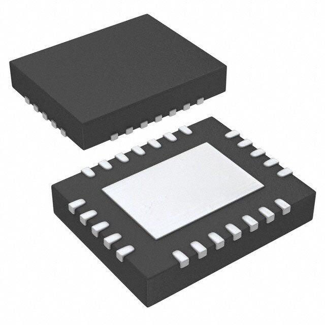
| 描述 | IC STEREO AUDIO 16BIT SER 24VQFN |
| 产品分类 | |
| 品牌 | Texas Instruments |
| 数据手册 | |
| 产品图片 |
|
| 产品型号 | PCM1870RHFR |
| PCN设计/规格 | |
| rohs | 无铅 / 符合限制有害物质指令(RoHS)规范要求 |
| 产品系列 | - |
| 产品培训模块 | http://www.digikey.cn/PTM/IndividualPTM.page?site=cn&lang=zhs&ptm=13240 |
| 产品目录页面 | |
| 供应商器件封装 | 24-VQFN(5x4) |
| 其它名称 | 296-21941-1 |
| 分辨率(位) | 16 b |
| 制造商产品页 | http://www.ti.com/general/docs/suppproductinfo.tsp?distId=10&orderablePartNumber=PCM1870RHFR |
| 包装 | 剪切带 (CT) |
| 安装类型 | 表面贴装 |
| 封装/外壳 | 24-VFQFN 裸露焊盘 |
| 工作温度 | -40°C ~ 85°C |
| 数据接口 | I²C, 串行, SPI™ |
| 标准包装 | 1 |
| 电压-电源 | 1.71 V ~ 3.6 V,2.4 V ~ 3.6 V |
| 电压源 | 模拟和数字 |
| 类型 | ADC, 音频 |
| 采样率(每秒) | 5k ~ 50k |


.jpg)


- 商务部:美国ITC正式对集成电路等产品启动337调查
- 曝三星4nm工艺存在良率问题 高通将骁龙8 Gen1或转产台积电
- 太阳诱电将投资9.5亿元在常州建新厂生产MLCC 预计2023年完工
- 英特尔发布欧洲新工厂建设计划 深化IDM 2.0 战略
- 台积电先进制程称霸业界 有大客户加持明年业绩稳了
- 达到5530亿美元!SIA预计今年全球半导体销售额将创下新高
- 英特尔拟将自动驾驶子公司Mobileye上市 估值或超500亿美元
- 三星加码芯片和SET,合并消费电子和移动部门,撤换高东真等 CEO
- 三星电子宣布重大人事变动 还合并消费电子和移动部门
- 海关总署:前11个月进口集成电路产品价值2.52万亿元 增长14.8%


PDF Datasheet 数据手册内容提取
(cid:2)(cid:17)(cid:14)(cid:14)(cid:20)(cid:2)(cid:14)(cid:13)(cid:18)(cid:12) (cid:4)(cid:14)(cid:13)(cid:8)(cid:17)(cid:7)(cid:16)(cid:15) (cid:10)(cid:14)(cid:13)(cid:11) (cid:5)(cid:9)(cid:19)(cid:6)(cid:15) (cid:3)(cid:12)(cid:15)(cid:16)(cid:14)(cid:17)(cid:11)(cid:9)(cid:12)(cid:16)(cid:15) PCM1870 SLAS544A–MAY2007–REVISEDSEPTEMBER2007 16-Bit Low-Power Stereo Audio ADC With Microphone Bias and Microphone Amplifier FEATURES • Package: 1 • AnalogFrontEnd: – 24-QFN(4mm· 5mm) – StereoSingleEndInputWithMUX – 24-DSBGA(2.49mm· 3.49mm) – MonoDifferentialInput • OperationTemperatureRange:–40(cid:176) Cto85(cid:176) C – StereoProgrammableGainAmplifier APPLICATIONS – MicrophoneBoostAmplifierandBias • PortableAudioPlayer,CellularPhone • AnalogPerformancesDynamicRange:90dB • VideoCamcorder,MovieDigitalStillCamera • Power-SupplyVoltage • PMP/DMB,VoiceRecorder – 1.71Vto3.6VforDigitalI/OSection – 1.71Vto3.6VforDigitalCoreSection DESCRIPTION – 2.4Vto3.6VforAnalogSection The PCM1870 is a low-power stereo ADC designed • LowPowerDissipation: for portable digital audio applications, with line-input – 13mWinRecord,1.8/2.4V,48kHz,Stereo amplifier, boost amplifier, microphone bias, programmable gain control, sound effects, and auto – 5.3mWinRecord,1.8/2.4V,8kHz,Mono level control (ALC). It is available in 24-QFN (4-mm · – 3.3μWinAllPowerDown 5-mm) and 24-DSBGA (2.49-mm · 3.49-mm) • SamplingFrequency:5kHzto50kHz packages to save footprint. The PCM1870 accepts • AutoLevelControlforRecording right-justified, left-justified, I2S, and DSP formats, providing easy interfacing to audio DSP and encoder • OperationbySingleClockInputWithoutPLL chips. Sampling rates up to 50 kHz are supported. • SystemClock:CommonAudioClock The user-programmable functions are accessible (256f /384f ),12/24,13/26,13.5/27,19.2/38.4, througha2-or3-wireserialcontrolport. S S 19.68/39.36MHz • 2(I2C)or3(SPI)WireSerialControl • ProgrammableFunctionbyRegisterControl: – DigitalSoftMute – PowerUp/DownControlforEachModule – 30-dBto–12-dBGainforAnalogInputs – 0/12/20-dBBoostforMicrophoneInput – ParameterSettingsforALC – Three-BandToneControland3DSound – High-PassFilterandTwo-StageNotchFilter • PopNoiseReductionCircuit 1 Pleasebeawarethatanimportantnoticeconcerningavailability,standardwarranty,anduseincriticalapplicationsof TexasInstrumentssemiconductorproductsanddisclaimerstheretoappearsattheendofthisdatasheet. PRODUCTIONDATAinformationiscurrentasofpublicationdate. Copyright©2007,TexasInstrumentsIncorporated Products conform to specifications per the terms of the Texas Instruments standard warranty. Production processing does not necessarilyincludetestingofallparameters.
PCM1870 www.ti.com SLAS544A–MAY2007–REVISEDSEPTEMBER2007 This integrated circuit can be damaged by ESD. Texas Instruments recommends that all integrated circuits be handled with appropriateprecautions.Failuretoobserveproperhandlingandinstallationprocedurescancausedamage. ESDdamagecanrangefromsubtleperformancedegradationtocompletedevicefailure.Precisionintegratedcircuitsmaybemore susceptibletodamagebecauseverysmallparametricchangescouldcausethedevicenottomeetitspublishedspecifications. ABSOLUTE MAXIMUM RATINGS overoperatingfree-airtemperaturerange(unlessotherwisenoted)(1) PCM1870 UNIT V ,V ,V Supplyvoltage –0.3to4 V DD IO CC Groundvoltagedifferences:DGND,AGND,PGND ±0.1 V Inputvoltage –0.3to4 V Inputcurrent(anypinsexceptsupplies) ±10 mA Ambienttemperatureunderbias –40to110 (cid:176) C Storagetemperature –55to150 (cid:176) C Junctiontemperature 150 (cid:176) C Leadtemperature(soldering) 260/5 (cid:176) C/s Packagetemperature(reflow,peak) 260 (cid:176) C (1) Stressesbeyondthoselistedunderabsolutemaximumratingsmaycausepermanentdamagetothedevice.Thesearestressratings only,andfunctionaloperationofthedeviceattheseoranyotherconditionsbeyondthoseindictedunderrecommendedoperating conditionsisnotimpled.Exposuretoabsolute-maximum-ratedconditionsforextendedperiodsmayaffectdevicereliabiltiy. RECOMMENDED OPERATING CONDITIONS MIN NOM MAX UNIT V Analogsupplyvoltage 2.4 3.3 3.6 V CC V ,V Digitalsupplyvoltage 1.71 3.3 3.6 V DD IO Digitalinputlogicfamily CMOS SCKIsystemclock 3.072 18.432 MHz Digitalinputclockfrequency LRCKsamplingclock 8 48 kHz Digitaloutputloadcapacitance 10 pF T Operatingfree-airtemperature –40 85 (cid:176) C A 2 SubmitDocumentationFeedback Copyright©2007,TexasInstrumentsIncorporated ProductFolderLink(s):PCM1870
PCM1870 www.ti.com SLAS544A–MAY2007–REVISEDSEPTEMBER2007 ELECTRICAL CHARACTERISTICS AllspecificationsatT =25(cid:176) C,V =V =V =V =3.3V,f =48kHz,systemclock=256f ,and16-bitdata,unless A DD IO CC PA S S otherwisenoted PCM1870RHF,PCM1870YZF PARAMETER TESTCONDITIONS UNIT MIN TYP MAX AUDIODATA DataFormat Resolution 16 Bits Audiodatainterfaceformat I2S,left-,right-justified,DSP Audiodatabitlength 16 Bits Audiodataformat MSB-first,2s-complement f Samplingfrequency 5 50 kHz S V <2V 27 DD Systemclock MHz V >2V 40 DD DIGITALINPUT/OUTPUT Logicfamily CMOScompatible V 0.7V IH IO Inputlogiclevel VDC V 0.3V IL IO I V =3.3V 10 IH IN Inputlogiccurrent μA I V =0V –10 IL IN V I =–2mA 0.75V OH OH IO Outputlogiclevel VDC V I =2mA 0.25V OL OL IO LINEINPUTTODIGITALOUTPUTTHROUGHADC(AIN1L/R,AIN2L/RANDPGINL/R—ALC=OFF,PG1=PG2=PG3=PG4=0dB DynamicPerformance 2.828 Vp-p Full-scaleinputvoltage 0dB 1 Vrms Dynamicrange EIAJ,A-weighted 90 dB SNR Signal-to-noiseratio EIAJ,A-weighted 83 90 dB Channelseparation 87 dB THD+N Totalharmonicdistortion+noise –1dB 0.009% 0.017% AnalogInput Centervoltage 0.5V V CC AIN1L,AIN1R,AIN2L,andAIN2R 10 20 Inputimpedance PGINLandPGINR,PG3=PG4=–12dB 70 142 kΩ PGINLandPGINR,PG3=PG4=30dB 4.7 9.5 ANALOGOUTPUTS(AOLANDAOR) Centervoltage 0.5V V CC Loadresistance 10 kΩ Loadcapacitance 20 pF MICROPHONEBIAS—ALC=OFF,PG1=PG2=PG3=PG4=0dB Biasvoltage 0.75V V CC Biassourcecurrent 2 mA Outputnoise 6.5 μV Copyright©2007,TexasInstrumentsIncorporated SubmitDocumentationFeedback 3 ProductFolderLink(s):PCM1870
PCM1870 www.ti.com SLAS544A–MAY2007–REVISEDSEPTEMBER2007 ELECTRICAL CHARACTERISTICS (continued) AllspecificationsatT =25(cid:176) C,V =V =V =V =3.3V,f =48kHz,systemclock=256f ,and16-bitdata,unless A DD IO CC PA S S otherwisenoted PCM1870RHF,PCM1870YZF PARAMETER TESTCONDITIONS UNIT MIN TYP MAX FILTERCHARACTERISTICS DecimationFilterforADC Passband 0.408f S Stopband 0.591f S Pass-bandripple ±0.02 dB Stop-bandattenuation f<3.268f –60 dB S Groupdelay 17/f s S High-PassFilterforADC –3dB 3.74 Frequencyresponse(f =4Hz) –0.5dB 10.66 Hz c –0.1dB 24.20 –3dB 118.77 Frequencyresponse(f =120Hz) –0.5dB 321.75 Hz c –0.1dB 605.52 –3dB 235.68 Frequencyresponse(f =240Hz) –0.5dB 609.95 Hz c –0.1dB 2601.2 POWERSUPPLYANDSUPPLYCURRENT V V 1.71 3.3 3.6 IO IO V Voltagerange V 1.71 3.3 3.6 VDC DD DD V V 2.4 3.3 3.6 CC CC BPZinput,allactive,noload 8 12 mA Supplycurrent Allinputsareheldstatic. 1 10 μA BPZinput 26.4 39.6 mW Powerdissipation Allinputsareheldstatic. 3.3 33 μW TEMPERATURECONDITION Operationtemperature –40 85 (cid:176) C θ Thermalresistance 35 (cid:176) C/W JA 4 SubmitDocumentationFeedback Copyright©2007,TexasInstrumentsIncorporated ProductFolderLink(s):PCM1870
PCM1870 www.ti.com SLAS544A–MAY2007–REVISEDSEPTEMBER2007 PIN ASSIGNMENTS RHF Package YZF Package (Top View) (Top View) AGND VCC MICB AIN1L AIN1R A AIN1R AIN1L MICB V COM 24 23 22 21 20 B V 1 19 PGINL COM PGINR PGINL V AGND CC AIN2R 2 18 AOL C AIN2L 3 17 PGINR AOR AOL AIN2R AIN2L MODE 4 16 AOR D MS/ADR 5 15 TEST TEST MODE MS/ADRMD/SDA MD/SDA 6 14 LRCK E MC/SCL 7 13 BCK LRCK DGND VIO MC/SCL 8 9 10 11 12 F BCK SCKI V DOUT DD UT VIO VDD ND CKI 1 2 3 4 O G S D D P0057-01 Table1. TERMINALFUNCTIONS TERMINAL NO. I/O DESCRIPTION NAME RHF YZF AGND 24 B4 – Groundforanalog AIN1L 21 A2 I Analoginput1forL-channel AIN1R 20 A1 I Analoginput1forR-channel AIN2L 3 C4 I Analoginput2forL-channel AIN2R 2 C3 I Analoginput2forR-channel AOL 18 C2 O MicrophoneamplifieroutputforL-channel AOR 16 C1 O MicrophoneamplifieroutputforR-channel BCK 13 F1 I/O Serialbitclock DGND 11 E2 – Groundfordigital DOUT 8 F4 O Serialaudiodataoutput LRCK 14 E1 I/O Left-andright-channelclock MC/SCL 7 E4 I Modecontrolclockfor3-wire/2-wireinterface MD/SDA 6 D4 I/O Modecontroldatafor3-wire/2-wireinterface MICB 22 A3 O Microphonebiassourceoutput MODE 4 D2 I 2-or3-wireinterfaceselection(LOW:SPI,HIGH:I2C) MS/ADR 5 D3 I Modecontrolselectfor3-wire/2-wireinterface PGINL 19 B2 I AnaloginputtogainamplifierforL-channel PGINR 17 B1 I AnaloginputtogainamplifierforR-channel SCKI 12 F2 I Systemclock TEST 15 D1 I TestPin.Shouldbeconnectedtoground. V 23 B3 – Powersupplyforanalog CC V 1 A4 – Commonvoltageforanalog COM V 10 F3 – Powersupplyfordigitalcore DD V 9 E3 – PowersupplyfordigitalI/O IO Copyright©2007,TexasInstrumentsIncorporated SubmitDocumentationFeedback 5 ProductFolderLink(s):PCM1870
PCM1870 www.ti.com SLAS544A–MAY2007–REVISEDSEPTEMBER2007 FUNCTIONALBLOCKDIAGRAM MD/SDA MC/SCL MS/ADR MODE AOL PGINL TEST SCKI DOUT BCK LRCK 2 Clock SerialInterface(SPI/IC) Manager AudioInterface Mute PG1 ATR AIN2L MUX1 3MUX AIN1L 0/+12/+20 dB ADL PG3 DS Digital D2S +30 to–12 dB ADC Filter ADR PG4 +30 to–12 dB DS Digital ADC Filter AIN1R 2 PG2 X 4 U X M U AIN2R M MCB 0/+12/+20 dB ModuleThatCanBePoweredUp/Down MicBias MICB PowerOn PowerUp/Down CCOOMM Reset Manager V V COM COM AOR PGINR V V DGND V AGND IO DD CC B0231-01 6 SubmitDocumentationFeedback Copyright©2007,TexasInstrumentsIncorporated ProductFolderLink(s):PCM1870
PCM1870 www.ti.com SLAS544A–MAY2007–REVISEDSEPTEMBER2007 TYPICAL PERFORMANCE CURVES AllspecificationsatT =25(cid:176) C,V =V =V =V =3.3V,f =8kHzto48kHz,systemclock=256f and16-bitdata, A DD IO CC PA S S unlessotherwisenoted. DECIMATIONFILTER,STOP-BAND DECIMATIONFILTER,PASS-BAND 0 0.2 –20 0.1 –40 B B d d – – e e d –60 d 0 u u plit plit m m A –80 A –0.1 –100 –120 –0.2 0 1 2 3 4 0 0.1 0.2 0.3 0.4 0.5 Frequency[´f ] Frequency[´f ] S S G001 G002 Figure1. Figure2. HIGH-PASSFILTERPASS-BANDCHARACTERISTICS HIGH-PASSFILTERPASS-BANDCHARACTERISTICS (f =4Hzat48kHz) (f =120Hzat48kHz) C C 5 5 0 0 B B d –5 d –5 – – e e d d u u plit plit m –10 m –10 A A –15 –15 –20 –20 0 0.0005 0.001 0.0015 0.002 0 0.005 0.01 0.015 0.02 Frequency[´f ] Frequency[´f ] S S G003 G012 Figure3. Figure4. Copyright©2007,TexasInstrumentsIncorporated SubmitDocumentationFeedback 7 ProductFolderLink(s):PCM1870
PCM1870 www.ti.com SLAS544A–MAY2007–REVISEDSEPTEMBER2007 TYPICAL PERFORMANCE CURVES (continued) AllspecificationsatT =25(cid:176) C,V =V =V =V =3.3V,f =8kHzto48kHz,systemclock=256f and16-bitdata, A DD IO CC PA S S unlessotherwisenoted. HIGH-PASSFILTERPASS-BANDCHARACTERISTICS (f =240Hzat48kHz) C 5 0 B d –5 – e d u plit m –10 A –15 –20 0 0.01 0.02 0.03 0.04 Frequency[´f ] S G004 Figure5. 8 SubmitDocumentationFeedback Copyright©2007,TexasInstrumentsIncorporated ProductFolderLink(s):PCM1870
PCM1870 www.ti.com SLAS544A–MAY2007–REVISEDSEPTEMBER2007 TYPICAL PERFORMANCE CURVES (continued) AllspecificationsatT =25(cid:176) C,V =V =V =V =3.3V,f =44.1kHz,systemclock=256f and16-bitdata,unless A DD IO CC PA S S otherwisenoted. 3BANDTONECONTROL(BASS,MID,TREBLE) 3BANDTONECONTROL(BASS) 15 15 10 10 5 5 B B d d – – e e d 0 d 0 u u plit plit m m A –5 A –5 –10 –10 –15 –15 0.01 0.1 1 10 100 1k 10k 100k 0 200 400 600 800 1k Frequency–Hz Frequency–Hz G005 G006 Figure6. Figure7. 3BANDTONECONTROL(MID) 3BANDTONECONTROL(TREBLE) 15 15 10 10 5 5 B B d d – – e e d 0 d 0 u u plit plit m m A –5 A –5 –10 –10 –15 –15 0 1k 2k 3k 4k 5k 2k 4k 6k 8k 10k 12k 14k Frequency–Hz Frequency–Hz G007 G008 Figure8. Figure9. Copyright©2007,TexasInstrumentsIncorporated SubmitDocumentationFeedback 9 ProductFolderLink(s):PCM1870
PCM1870 www.ti.com SLAS544A–MAY2007–REVISEDSEPTEMBER2007 TYPICAL PERFORMANCE CURVES (continued) AllspecificationsatT =25(cid:176) C,V =V =V =V =3.3V,f =48kHz,systemclock=256f and16-bitdata,unless A DD IO CC PA S S otherwisenoted. ADCSNRATHIGHGAIN(PG1/PG2=0dB) ADCSNRATHIGHGAIN(PG1/PG2=20dB) 100 90 85 f =1kHz IN 90 80 SingleInput 75 85 SingleInput B B 70 d DifferentialInput d – 70 – 65 R R N N S S 60 60 DifferentialInput 55 50 50 f =1kHz 45 IN 40 40 0 5 10 15 20 25 30 0 5 10 15 20 25 30 PG3/PG4Gain–dB PG3/PG4Gain–dB G009 G010 Figure10. Figure11. THD+N/SNRvsPOWERSUPPLY (ADCTODIGITALOUTPUT) 0.012 92 f =1kHz IN 0.011 91 THD+N %0.010 90 B – d N – + R D N TH0.009 89 S SNR 0.008 88 0.007 87 2 2.5 3 3.5 4 PowerSupply–V G011 Figure12. 10 SubmitDocumentationFeedback Copyright©2007,TexasInstrumentsIncorporated ProductFolderLink(s):PCM1870
PCM1870 www.ti.com SLAS544A–MAY2007–REVISEDSEPTEMBER2007 PCM1870 DESCRIPTION AnalogInput The AIN1L, AIN1R, AIN2L and AIN2R pins can be used as microphone or line inputs with selectable 0- or 20-dB boost and 1-Vrms input. All analog inputs have high input impedance (20 kΩ), which is not changed by gain settings. One pair of inputs is selected by register 87 (AIL[1:0], AIR[1:0]). AIN1L and AIN1R can also be used as amonauraldifferentialinput. GainSettingforAnalogInput Analog signals can be adjusted from 30 dB to –12 dB in 1-dB steps after the 0-, 12- or 20-dB boost amplifier. Gainlevelcanbesetforeachchannelbyregister79,80(ALV[5:0],ARV[5:0]). A/DConverter The ADC includes a multilevel delta-sigma modulator, aliasing filter, decimation filter, high-pass filter and notch filter and can accept 1 Vrms as full-scale input voltage. The decimation filter has a digital soft mute controlled by register 81 (RMUL, RMUR), and the high-pass and notch filters can be disabled by register 81 (HPF[1:0]) and registers96through104iftheyarenotneededtocanceldcoffsetoravoidwindnoise. CommonVoltage Unbuffered common voltage. The V pin is normally biased to 0.5 V , and it provides common voltage to COM CC internalcircuitry.Connectinga4.7-μFcapacitortothispinisrecommendedtooptimizeanalogperformance. MicrophoneBias The MICB pin is a microphone bias source for an external microphone, which can provide 2 mA (typ) bias current. AutoLevelControl(ALC)forRecording The sound when microphone recording should be adjusted to a suitable level without saturation. The digitally controlled auto level control (ALC) automatically expands small input signals and compresses large input signals while recording. Expansion level, compression level, attack time, and recovery time can be selected by register 83.Seethebitdescriptionsofregister83fordetailedsettings. 3DSound A 3D sound effect is provided by mixing L-channel and R-channel data through a band-pass filter with two control parameters, mixing ratio and band-pass filter characteristic. The control parameters are set in register 95 (3DP[3:0],3FLO).The3DsoundeffectisappliedtotheADCdigitaloutput. 3-BandToneControl Tonecontrolhasbass,midrange,andtreblecontrolsthat can be adjusted from 12 dB to –12 dB in 1-dB steps by register 92 to 94 (LGA[4:0], MGA[4:0] and HGA[4:0]). Register 92 (LPAE), which attenuates the digital input signal automatically, can prevent clipping of the output signal at settings higher than 0 dB for bass control. LPAE isnoteffectiveformidrangeandtreblecontrol. High-PassFilterandNotchFilter The high-pass filter cuts dc offset in the analog section of the ADC and can be set to 4 Hz, 120 Hz, or 240 Hz at 48-kHzsamplingbyregister81(HPF[1:0]). Notch filters remove noise at particular frequencies, CCD noise, motor noise and other mechanical noise in an application. The PCM1870 has two notch filters, whose center frequency and frequency bandwidth can be programmedbyregisters96to104. DigitalMonauralMixing The audio data can be mixed to monaural digital data from stereo digital data in the internal audio interface sectionbyregister96(MXEN). Copyright©2007,TexasInstrumentsIncorporated SubmitDocumentationFeedback 11 ProductFolderLink(s):PCM1870
PCM1870 www.ti.com SLAS544A–MAY2007–REVISEDSEPTEMBER2007 Zero-CrossDetection Zero-cross detection minimizes audible zipper noise while changing analog volume and digital attenuation. This functioncanbeappliedtodigitalinputordigitaloutputbyregister86(ZCRS). PowerUp/DownforEachModule Using register 73 (PBIS), register 82 (PAIR, PAIL, PADS, PMCB, PADR, PADL), and register 90 (PCOM), unusedmodulescanbepowereddowntominimizepowerconsumption(13mWwhenrecordingonly). DigitalInterface All digital I/O pins can interface at various power supply voltages. The V pin can be connected to a 1.71-V to IO 3.6-Vpowersupply. PowerSupply The V pin can be connected to 2.4 V to 3.6 V. The V pin and V pin can be connected to 1.71 to 3.6 V. A CC DD IO differentvoltagecanbeappliedtoeachofthesepins(forexample,V =1.8V,V =3.3V). DD IO 12 SubmitDocumentationFeedback Copyright©2007,TexasInstrumentsIncorporated ProductFolderLink(s):PCM1870
PCM1870 www.ti.com SLAS544A–MAY2007–REVISEDSEPTEMBER2007 DESCRIPTION OF OPERATION SystemClockInput The PCM1870 can accept input clocks of various frequencies without a PLL. The clocks are used for clocking of the digital filters, auto level control, and delta-sigma modulators, and classified into common-audio and application-specific clocks. Table 2 shows frequencies of the common audio clock and the application-specific clock. Figure 13 shows timing requirements for system clock inputs. The sampling rate and frequency of the system clock are determined by settings in register 86 (MSR[2:0]) and register 85 (NPR[5:0]). Note that the samplingrateoftheapplication-specificclockhasalittlesamplingerror.ThedetailsareshowninTable8. Table2.FrequencyofCommonAudioClock FREQUENCY Commonaudioclock 11.2896,12.288,16.9344,18.432MHz Application-specificclock 12,13,13.5,24,26,27,19.2,19.68,38.4,39.36MHz t w(SCKH) 0.7 V IO SCKI 0.3 V IO t w(SCKL) T0005-12 PARAMETERS SYMBOL MIN UNIT Systemclockpulseduration,high t 14 ns w(SCKH) Systemclockpulseduration,low t 14 ns w(SCKL) Figure13.SystemClockTiming Power-OnResetandSystemReset The power-on-reset circuit outputs reset signal, typically at V = 1.2 V, and this circuit does not depend on the DD voltage of other power-supplies (V , V , and V ). Internal circuits are cleared to default status, then signals CC PA IO are removed from all analog and digital outputs. The PCM1870 does not require any power supply sequencing. Registerdatamustbewrittenafterturningallpowersupplieson. System reset is enabled by setting register 85 (SRST), and all registers are cleared automatically. All circuits are reset to their default status at once. Note that the PCM1870 has audible pop noise on the analog outputs when enablingSRST. PowerOn/OffSequence To reduce audible pop noise, a sequence of register settings is required after turning all power supplies on when powering up, or before turning the power supplies off when powering down. If some modules are not required for a particular application or operation, they should be placed in the power-down state after performing the power-on sequence. The recommended power-on and power-off sequences are shown in Table 3 and Table 4, respectively. Copyright©2007,TexasInstrumentsIncorporated SubmitDocumentationFeedback 13 ProductFolderLink(s):PCM1870
PCM1870 www.ti.com SLAS544A–MAY2007–REVISEDSEPTEMBER2007 Table3.RecommendedPower-OnSequence REGISTER STEP NOTE SETTINGS 1 — TurnONallpowersupplies(1) 2 5102 ADCaudiointerfaceformat(left-justified) (2) H 3 5A00 PG1,PG2gaincontrol(0dB) H 4 4980 Analogbiaspowerup H 5 5601 Zero-crossdetectionenable H 6 4A01 V powerup H COM 7 523F Analogfrontend(ADL,ADR,D2S,MCB,PG1,2,5,6)powerup H 8 5711 Analoginput(MUX3,MUX4)select.Analoginput(MUX1,MUX2)select H 9 4F0C AnaloginputL-ch(PG3)volume(0dB)(3) H 10 500C AnaloginputR-ch(PG4)volume(0dB)(3) H (1) V shouldbeturnedonfirstoratthesametimewithotherpowersupplies.Itisrecommendedtosettheregisterdataafterturningon DD allpowersuppliesandwhilethesystemclockisrunning. (2) TheaudiointerfaceformatshouldbesettomatchtheDSPordecoderbeingused. (3) Anylevelisacceptableforvolumeorattenuation.Thelevelshouldreturntothatrecordedintheregisterdatawhensystemwaslast poweredoff. Table4.RecommendedPower-OffSequence REGISTER STEP NOTE SETTINGS 1 5132 ADCL-ch/R-chdigitalsoftmuteenable,ADCaudiointerfaceformat(left-justified)(1) H 2 5200 Analogfrontend(ADL,ADR,D2S,MCB,PG1,2,5,6)powerdown H 3 4A00 V powerdown H COM 4 4900 Analogbiaspowerdown H 5 — TurnOFFallpowersupplies. (2) (1) TheaudiointerfaceformatshouldbesettomatchtheDSPordecoderbeingused. (2) Power-supplysequencingisnotrequired.Itisrecommendedtomaketherequiredregistersettingswhilethesystemclockisrunning, thenturnoffallpowersupplies. 14 SubmitDocumentationFeedback Copyright©2007,TexasInstrumentsIncorporated ProductFolderLink(s):PCM1870
PCM1870 www.ti.com SLAS544A–MAY2007–REVISEDSEPTEMBER2007 Power-SupplyCurrent The current consumption of the PCM1870 depends on the power-up/down status of each circuit module. In order to save power consumption, disabling each module is recommended when it is not used in an appliction or operation.Table5showscurrentconsumtptioninsomestates. Table5.PowerConsumptionTable POWERSUPPLYCURRENT[mA] PD[mW] OPERATIONMODE V V V V TOTAL TOTAL DD DD CC IO (1.8V) (3.3V) (3.3V) (3.3V) (V =1.8V) (V =3.3V) DD DD ALLPOWERDOWN 0.000 0.000 0.001 0.000 0.003 0.003 Recording(f =48kHz) S Lineinput(AIN2L/AIN2R) 1.78 3.71 4.58 0.10 18.3 27.7 Micinput(AIN1L/AIN1R,20dB) 1.79 3.71 5.06 0.10 19.9 29.3 Micinput(AIN1L/AIN1R,20dB)withALC 2.73 5.59 5.06 0.10 21.6 35.5 Monomicinput(AIN1L,20dB) 1.33 2.80 3.56 0.10 14.1 21.3 Monomicinput(AIN1L,20dB)withALC 2.21 4.60 3.56 0.10 15.7 27.3 Monodiffmicinput(AIN1L/AIN1R,20dB) 1.33 2.80 3.88 0.10 15.2 22.4 Monodiffmicinput(AIN1L/AIN1R,20dB)withALC 2.21 4.60 3.88 0.10 16.8 28.3 Recording(f =22.05kHz) S Lineinput(AIN2L/AIN2R) 0.82 1.66 3.71 0.10 13.7 18.1 Micinput(AIN1L/AIN1R,20dB) 0.82 1.66 4.20 0.10 15.3 19.7 Micinput(AIN1L/AIN1R,20dB)withALC 1.26 2.55 4.20 0.10 16.1 22.6 Monomicinput(AIN1L,20dB) 0.61 1.23 2.74 0.10 10.1 13.4 Monomicinput(AIN1L,20dB)withALC 1.03 2.10 2.74 0.10 10.9 1.63 Monodiffmicinput(AIN1L/AIN1R,20dB) 0.61 1.23 3.06 0.10 11.2 14.5 Monodiffmicinput(AIN1L/AIN1R,20dB)withALC 1.02 2.08 3.06 0.10 11.9 17.3 Recording(f =16kHz) S Lineinput(AIN2L/AIN2R) 0.59 1.18 3.51 0.10 12.7 15.8 Micinput(AIN1L/AIN1R,20dB) 0.59 1.18 3.99 0.10 14.2 17.4 Micinput(AIN1L/AIN1R,20dB)withALC 0.91 1.85 3.99 0.10 14.8 19.6 Monomicinput(AIN1L,20dB) 0.44 0.87 2.55 0.10 9.2 11.6 Monomicinput(AIN1L,20dB)withALC 0.75 1.52 2.55 0.10 9.8 13.8 Monodiffmicinput(AIN1L/AIN1R,20dB) 0.44 0.87 2.87 0.10 10.3 12.7 Monodiffmicinput(AIN1L/AIN1R,20dB)withALC 0.74 1.50 2.87 0.10 10.8 14.8 Recording(f =8kHz) S Lineinput(AIN2L/AIN2R) 0.29 0.54 3.23 0.10 11.2 12.8 Micinput(AIN1L/AIN1R,20dB) 0.29 0.54 3.72 0.10 12.8 14.4 Micinput(AIN1L/AIN1R,20dB)withALC 0.46 0.88 3.72 0.10 13.1 15.5 Monomicinput(AIN1L,20dB) 0.22 0.39 2.29 0.10 8.0 9.2 Monomicinput(AIN1L,20dB)withALC 0.37 0.70 2.29 0.10 8.2 10.2 Monodiffmicinput(AIN1L/AIN1R,20dB) 0.22 0.39 2.61 0.10 9.0 10.2 Monodiffmicinput(AIN1L/AIN1R,20dB)withALC) 0.37 0.70 2.61 0.10 9.3 11.3 Condition:256f ,16bits,slavemode,zerodatainput,noload S Copyright©2007,TexasInstrumentsIncorporated SubmitDocumentationFeedback 15 ProductFolderLink(s):PCM1870
PCM1870 www.ti.com SLAS544A–MAY2007–REVISEDSEPTEMBER2007 AudioSerialInterface The audio serial interface of the PCM1870 consists of LRCK, BCK and DOUT. Sampling rate (f ), left and right S channel are present on LRCK. DOUT transmits the serial data from the decimation filter for the ADC. BCK is used to transmit the serial audio data on DOUT at its high-to-low transition. BCK and LRCK should be synchronizedwithaudiosystemclock.Ideally,itisrecommendedthattheyarederivedfromit. The PCM1870 requires LRCK to be synchronized with the system clock. The PCM1870 do not need a specific phaserelationshipbetweenLRCKandthesystemclock. The PCM1870 has both master mode and slave mode interface formats, which can be selected by register 84 (MSTR).LRCKandBCKaregeneratedfromthesystemclockinmastermode. AudioDataFormatsandTiming The PCM1870 supports I2S, right-justified, left-justified, and DSP formats. The data formats are shown in Figure 16, and they are selected using resister 70 (RFM[1:0], PFM[1:0]). All formats require binary 2s-complement,MSB-firstaudiodata.ThedefaultformatisI2S.Figure14showsadetailedtimingdiagram. LRCK 50% of V IO t w(BCL) t t w(BCH) (LB) BCK 50% of V IO t (BL) t (BCY) t t (CKDO) (LRDO) DOUT 50% of V IO T0010-12 PARAMETERS SYMBOL MIN MAX UNIT BCKpulsecycletime(I2S,left-andright-justifiedformats) t 1/(64f )(1) (BCY) S BCKpulsecycletime(DSPformat) t 1/(256f )(1) (BCY) S BCKhigh-leveltime t 35 ns w(BCH) BCKlow-leveltime t 35 ns w(BCL) BCKrisingedgetoLRCKedge t 10 ns (BL) LRCKedgetoBCKrisingedge t 10 ns (LB) DOUTdelaytimefromBCKfallingedge t 40 ns (CKDO) (1) f isthesamplingfrequency. S Figure14.AudioInterfaceTiming(SlaveMode) 16 SubmitDocumentationFeedback Copyright©2007,TexasInstrumentsIncorporated ProductFolderLink(s):PCM1870
PCM1870 www.ti.com SLAS544A–MAY2007–REVISEDSEPTEMBER2007 t (SCY) SCKI 50% of V IO t (DL) LRCK (Output) 50% of V IO t w(BCL) t t t w(BCH) (DB) (DB) BCK (Output) 50% of V IO t (BCY) DOUT 50% of V IO t (DS) t (DH) T0011-05 PARAMETERS SYMBOL MIN MAX UNIT SCKIpulsecycletime t 1/(256f )(1) (SCY) S LRCKedgefromSCKIrisingedge t 5 140 ns (DL) BCKedgefromSCKIrisingedge t 5 140 ns (DB) BCKpulsecycletime t 1/(64f )(1) (BCY) S BCKhigh-leveltime t 146 ns w(BCH) BCKlow-leveltime t 146 ns w(BCL) DOUTsetuptime t 10 ns (DS) DOUTholdtime t 10 ns (DH) (1) f isupto48kHz.f isthesamplingfrequency S S Figure15.AudioInterfaceTiming(MasterMode) Copyright©2007,TexasInstrumentsIncorporated SubmitDocumentationFeedback 17 ProductFolderLink(s):PCM1870
PCM1870 www.ti.com SLAS544A–MAY2007–REVISEDSEPTEMBER2007 (a) Right-Justified Data Format; L-Channel = HIGH, R-Channel = LOW 1/fS LRCK L-Channel R-Channel BCK (1) (= 32 fS, 48 fS, or 64 fS) 16-Bit Right-Justified DOUT 15 16 1 2 3 4 5 6 7 8 9 10 11 12 13 14 15 16 1 2 3 4 5 6 7 8 9 10 11 12 13 14 15 16 MSB LSB MSB LSB 2 (b) I S Data Format; L-Channel = LOW, R-Channel = HIGH 1/fS LRCK L-Channel R-Channel BCK (1) (= 32 fS, 48 fS, or 64 fS) DOUT 1 2 3 4 5 6 7 8 9 10 11 12 13 14 15 16 1 2 3 4 5 6 7 8 9 10 11 12 13 14 15 16 1 2 MSB LSB MSB LSB (c) Left-Justified Data Format; L-Channel = HIGH, R-Channel = LOW 1/fS LRCK L-Channel R-Channel BCK (1) (= 32 fS, 48 fS, or 64 fS) DOUT 1 2 3 4 5 6 7 8 9 10 11 12 13 14 15 16 1 2 3 4 5 6 7 8 9 10 11 12 13 14 15 16 1 2 MSB LSB MSB LSB (d) Burst BCK Interface Format in Master Mode; L-Channel = HIGH, R-Channel = LOW 1/fS LRCK L-Channel R-Channel BCK (1) (= 32 fS, 48 fS, or 64 fS) DOUT 1 2 3 4 5 6 7 8 9 10 11 12 13 14 15 16 1 2 3 4 5 6 7 8 9 10 11 12 13 14 15 16 1 2 MSB LSB MSB LSB (e) DSPFormat 1/fS LRCK BCK (= 32 fS, 48 fS,64 fS, 128 fSor 256 fS) DOUT 1 2 3 4 5 6 7 8 9 10 11 12 13 14 15 16 1 2 3 4 5 6 7 8 9 10 11 12 13 14 15 16 1 2 MSB LSB MSB LSB T0009-09 (1) AllaudiointerfaceformatssupportBCK=64f inmastermode(register69,MSTR=1).Whensettomultisampling S rate,f ofBCKissettohalftherateoftheDSMoperationfrequency. S Figure16.AudioDataOutputFormats 18 SubmitDocumentationFeedback Copyright©2007,TexasInstrumentsIncorporated ProductFolderLink(s):PCM1870
PCM1870 www.ti.com SLAS544A–MAY2007–REVISEDSEPTEMBER2007 THREE-WIRE INTERFACE (SPI, MODE (PIN 28) = LOW) All write operations for the serial control port use 16-bit data words. Figure 17 shows the control data word format. The most significant bit must be 0. There are seven bits, labeled IDX[6:0], that set the register address for the write operation. The least-significant eight bits, D[7:0], contain the data to be written to the register specifiedbyIDX[6:0]. Figure 18 shows the functional timing diagram for writing to the serial control port. To write the data into the mode register, the data is clocked into an internal shift register on the rising edge of the MC clock. The serial data should change on the falling edge of the MC clock and should be LOW during write mode. The rising edge of MS should be aligned with the falling edge of the last MC clock pulse in the 16-bit frame. The MC can run continuouslybetweentransactionswhileMSisintheLOWstate. MSB LSB 000 IDX6 IDX5 IDX4 IDX3 IDX2 IDX1 IDX0 D7 D6 D5 D4 D3 D2 D1 D0 Register Index (or Address) Register Data R0001-01 Figure17.ControlDataWordFormatforMD (1) Single Write Operation 16 Bits MS MC MD MSB LSB MSB (2) Continuous Write Operation 8 Bits x N Frames MS MC MD MSB LSB MSB LSB MSB LSB MSB LSB RegisterIndex Register (N) Data Register (N+1) Data Register (N+2) Data 8 Bits N Frames T0012-03 Figure18.RegisterWriteOperation Copyright©2007,TexasInstrumentsIncorporated SubmitDocumentationFeedback 19 ProductFolderLink(s):PCM1870
PCM1870 www.ti.com SLAS544A–MAY2007–REVISEDSEPTEMBER2007 Three-WireInterface(SPI)TimingRequirements Figure 19 shows a detailed timing diagram for the serial control interface. These timing parameters are critical for propercontrolportoperation. tw(MHH) MS 50% of VIO t(MLS) tw(MCL) tw(MCH) t(MLH) MC 50% of VIO t(MCY) LSB MD 50% of VIO t(MDS) t(MDH) T0013-08 PARAMETERS SYMBOL MIN TYP MAX UNIT MCpulsecycletime t 500(1) ns (MCY) MClow-leveltime t 50 ns w(MCL) MChigh-leveltime t 50 ns w(MCH) MShigh-leveltime t See(1) ns w(MHH) MSfallingedgetoMCrisingedge t 50 ns (MLS) MSholdtime t 20 ns (MLH) MDholdtime t 15 ns (MDH) MDsetuptime t 20 ns (MDS) (1) 3/(128f )s(min),wheref isthesamplingfrequency S S A Figure19.SPIInterfaceTiming 20 SubmitDocumentationFeedback Copyright©2007,TexasInstrumentsIncorporated ProductFolderLink(s):PCM1870
PCM1870 www.ti.com SLAS544A–MAY2007–REVISEDSEPTEMBER2007 TWO-WIRE INTERFACE [I2C, MODE (PIN 28) = HIGH] The PCM1870 supports the I2C serial bus and the data transmission protocol for the I2C standard as a slave device.ThisprotocolisexplainedinI2Cspecification2.0. InI2Cmode,thecontrolterminalsarechangedasfollows. TERMINALNAME PROPERTY DESCRIPTION MS/ADR Input I2Caddress MD/SDA Input/output I2Cdata MC/SCL Input I2Cclock SlaveAddress MSB LSB 1 0 0 0 1 1 ADR R/W The PCM1870 has its 7-bit slave address. The first six bits (MSBs) of the slave address are factory preset to 100011. The next bit of the address byte is the device select bit, which can be user-defined by ADR terminal. A maximum of two PCM1870s can be connected on the same bus at one time. Each PCM1870 responds when it receivesitsownslaveaddress. PacketProtocol A master device must control packet protocol, which is start condition, slave address with read/write bit, data if write or acknowledgement if read, and stop condition. The PCM1870 supports only slave-receiver and slave-transmitter. SDA SCL St 1−7 8 9 1−8 9 1−8 9 Sp Slave Address R/W ACK DATA ACK DATA ACK R/W: Read Operation if 1; Otherwise, Write Operation Start ACK: Acknowledgement of a Byte if 0 Stop Condition Condition DATA: 8 Bits (Byte) Write Operation Transmitter M M M S M S M S M Data Type St Slave Address R/W ACK DATA ACK DATA ACK Sp Read Operation Transmitter M M M S S M S M M Data Type St Slave Address R/W ACK DATA ACK DATA NACK Sp M: Master Device S: Slave Device St: Start Condition Sp: Stop Condition T0049-03 Figure20.BasicI2CFramework Copyright©2007,TexasInstrumentsIncorporated SubmitDocumentationFeedback 21 ProductFolderLink(s):PCM1870
PCM1870 www.ti.com SLAS544A–MAY2007–REVISEDSEPTEMBER2007 WriteOperation A master can write any PCM1870 registers using single access. The master sends a PCM1870 slave address withawritebit,aregisteraddress,andthedata.Whenundefinedregistersareaccessed,the PCM1870 does not sendanacknowledgement.TheFigure21showsadiagramofthewriteoperation. Transmitter M M M S M S M S M Data Type St Slave Address W ACK Reg Address ACK Write Data ACK Sp M: Master Device S: Slave Device St: Start Condition W: Write ACK: Acknowledge Sp: Stop Condition R0002-01 Figure21.FrameworkforWriteOperation ReadOperation A master can read the PCM1870 register. The value of the register address is stored in an indirect index register in advance. The master sends a PCM1870 slave address with a read bit after storing the register address. Then the PCM1870 transfers the data which the index register points to. Figure 22 shows a diagram of the read operation. Transmitter M M M S M S M M M S S M M Data Type St Slave Address W ACK Reg Address ACK Sr Slave Address R ACK Read Data NACK Sp M: Master Device S: Slave Device St: Start Condition Sr: Repeated Start Condition ACK: Acknowledge Sp: Stop Condition NACK: Not Acknowledge W: Write R: Read R0002-02 NOTE: Theslaveaddressaftertherepeatedstartconditionmustbethesameasthepreviousslaveaddress. Figure22.ReadOperation 22 SubmitDocumentationFeedback Copyright©2007,TexasInstrumentsIncorporated ProductFolderLink(s):PCM1870
PCM1870 www.ti.com SLAS544A–MAY2007–REVISEDSEPTEMBER2007 TimingDiagram Start Stop t(D-HD) t(SDA-F) t(BUF) t(D-SU) t(SDA-R) t(P-SU) SDA t(SCL-R) t(RS-HD) t(SP) t(LOW) SCL t(S-HD) t(HI) t(RS-SU) t(SCL-F) T0050-03 TIMINGCHARACTERISTICS SYMBOL PARAMETER CONDITIONS MIN MAX UNIT f SCLclockfrequency Standard 100 kHz SCL t BusfreetimebetweenaSTOPandSTARTcondition Standard 4.7 μs (BUF) t LowperiodoftheSCLclock Standard 4.7 μs (LOW) t HighperiodoftheSCLclock Standard 4 μs (HI) t SetuptimeforSTARTcondition Standard 4.7 μs (RS-SU) t HoldtimeforSTARTcondition Standard 4 μs (S-HD) t Datasetuptime Standard 250 ns (D-SU) t Dataholdtime Standard 0 900 ns (D-HD) t RisetimeofSCLsignal Standard 20+0.1C 1000 ns (SCL-R) B t FalltimeofSCLsignal Standard 20+0.1C 1000 ns (SCL-F) B t RisetimeofSDAsignal Standard 20+0.1C 1000 ns (SDA-R) B t FalltimeofSDAsignal Standard 20+0.1C 1000 ns (SDA-F) B t SetuptimeforSTOPcondition Standard 4 μs (P-SU) C CapacitiveloadforSDAandSCLline 400 pF B t Pulsedurationofspikesuppressed 25 ns (SP) Figure23.I2CInterfaceTiming Copyright©2007,TexasInstrumentsIncorporated SubmitDocumentationFeedback 23 ProductFolderLink(s):PCM1870
PCM1870 www.ti.com SLAS544A–MAY2007–REVISEDSEPTEMBER2007 USER-PROGRAMMABLE MODE CONTROLS RegisterMap Themodecontrolregistermapisshownin Table 6. Each register includes an index (or address) indicated by the IDX[6:0]bits. Table6.ModeControlRegisterMap IDX[6:0] REGISTER DESCRIPTION B7 B6 B5 B4 B3 B2 B1 B0 (B14–B8) Register73 49h Analogbiaspowerup/down PBIS RSV RSV RSV RSV RSV RSV RSV Register74 4Ah VCOMpowerup/down RSV RSV RSV RSV RSV RSV RSV PCOM Register79 4Fh VolumeforADCinput(L-ch) RSV RSV ALV5 ALV4 ALV3 ALV2 ALV1 ALV0 Register80 50h VolumeforADCinput(R-ch) RSV RSV ARV5 ARV4 ARV3 ARV2 ARV1 ARV0 Register81 51h ADChighpass-filter,softmute,audiointerface HPF1 HPF0 RMUL RMUR RSV DSMC RFM1 RFM0 Register82 52h ADC,MCB,PG1,2,5,6,D2Spowerup/down RSV RSV PAIR PAIL PADS PMCB PADR PADL Register83 53h Autolevelcontrolforrecording RALC RSV RRTC RATC RCP1 RCP0 RLV1 RLV0 Register84 54h Mastermode RSV RSV RSV RSV RSV MSTR RSV BIT0 Register85 55h Systemreset,samplingratecontrol SRST RSV NPR5 NPR4 NPR3 NPR2 NPR1 NPR0 Register86 56h BCKconfig,mastermode,zerocross MBST MSR2 MSR1 MSR0 RSV RSV RSV ZCRS Register87 57h Analoginputselect(MUX1,2,3,4) AD2S RSV AIR1 AIR0 RSV RSV AIL1 AIL0 Register90 5Ah VCOMpowerup/down,rampup/downtime,boost RSV RSV RSV RSV RSV RSV G20R G20L Register92 5Ch Bassboostgainlevel(200Hz) LPAE RSV RSV LGA4 LGA3 LGA2 LGA1 LGA0 Register93 5Dh Middleboostgainlevel(1kHz) RSV RSV RSV MGA4 MGA3 MGA2 MGA1 MGA0 Register94 5Eh Trebleboostgainlevel(5kHz) RSV RSV RSV HGA4 HGA3 HGA2 HGA1 HGA0 Register95 5Fh Soundeffectsourceselect,3Dsound RSV 3DEN RSV 3FL0 3DP3 3DP2 3DP1 3DP0 Register96 60h 2-stagenotchfilter,digitalmonauralmixing NEN2 NEN1 NUP2 NUP1 RSV RSV RSV MXEN Register97 61h 1st-stagenotchfilterlowercoefficient(a1) F107 F106 F105 F104 F103 F102 F101 F100 Register98 62h 1st-stagenotchfilteruppercoefficient(a1) F115 F114 F113 F112 F111 F110 F109 F108 Register99 63h 1st-stagenotchfilterlowercoefficient(a2) F207 F206 F205 F204 F203 F202 F201 F200 Register100 64h 1st-stagenotchfilteruppercoefficient(a2) F215 F214 F213 F212 F211 F210 F209 F208 Register101 65h 2nd-stagenotchfilterlowercoefficient(a1) S107 S106 S105 S104 S103 S102 S101 S100 Register102 66h 2nd-stagenotchfilteruppercoefficient(a1) S115 S114 S113 S112 S111 S110 S109 S108 Register103 67h 2nd-stagenotchfilterlowercoefficient(a2) S207 S206 S205 S204 S203 S202 S201 S200 Register104 68h 2nd-stagenotchfilteruppercoefficient(a2) S215 S214 S213 S212 S211 S210 S209 S208 Register124 7Ch Micboost RSV RSV RSV RSV RSV RSV G12R G12L ADC:A/Dconverter MCB:Microphonebias PGx:Analoginputbuffer D2S:Differentialtosingle-endedamplifier 24 SubmitDocumentationFeedback Copyright©2007,TexasInstrumentsIncorporated ProductFolderLink(s):PCM1870
PCM1870 www.ti.com SLAS544A–MAY2007–REVISEDSEPTEMBER2007 Register73 B15 B14 B13 B12 B11 B10 B9 B8 B7 B6 B5 B4 B3 B2 B1 B0 Register73 0 IDX6 IDX5 IDX4 IDX3 IDX2 IDX1 IDX0 PBIS RSV RSV RSV RSV RSV RSV RSV IDX[6:0]:1001001b(49h)Register73 PBIS:PowerUp/DownControlforBias Defaultvalue:0 Thisbitisusedtocontrolpowerup/downfortheanalogbiascircuit. PBIS=0 Powerdown(default) PBIS=1 Powerup Register74 B15 B14 B13 B12 B11 B10 B9 B8 B7 B6 B5 B4 B3 B2 B1 B0 Register74 0 IDX6 IDX5 IDX4 IDX3 IDX2 IDX1 IDX0 RSV RSV RSV RSV RSV RSV RSV PCOM IDX[6:0]:1001010b(4Ah)Register74 PCOM:PowerUp/DownControlforV COM Defaultvalue:0 Thisbitisusedtocontrolpowerup/downforV . COM PCOM=0 Powerdown(default) PCOM=1 Powerup Copyright©2007,TexasInstrumentsIncorporated SubmitDocumentationFeedback 25 ProductFolderLink(s):PCM1870
PCM1870 www.ti.com SLAS544A–MAY2007–REVISEDSEPTEMBER2007 Register79and80 B15 B14 B13 B12 B11 B10 B9 B8 B7 B6 B5 B4 B3 B2 B1 B0 Register79 0 IDX6 IDX5 IDX4 IDX3 IDX2 IDX1 IDX0 RSV RSV ALV5 ALV4 ALV3 ALV2 ALV1 ALV0 Register80 0 IDX6 IDX5 IDX4 IDX3 IDX2 IDX1 IDX0 RSV RSV ARV5 ARV4 ARV3 AR2 ARV1 ARV0 IDX[6:0]:1001111b(4Fh)Register79 IDX[6:0]:1010000b(50h)Register80 ALV[5:0]:GainControlforPG3(ADCAnalogInputR-Channel) ARV[5:0]:GainControlforPG4(ADCAnalogInputL-Channel) Defaultvalue:00 PG3 and PG4 can be independently controlled for ADC input from 30 dB to –12 dB in 1-dB steps. ADC output may have zipper noise when changing levels. In the PCM1870, the noise can be reduced when making the changebyusingzero-crossdetection(Register85,ZCRS). Table7.GainLevelSetting ALV[5:0],ARV[5:0] ALV[5:0],ARV[5:0] GAINLEVELSETTING GAINLEVELSETTING BINARY HEX BINARY HEX 101010 2A 30dB 010100 14 8dB 101001 29 29dB 010011 13 7dB 101000 28 28dB 010010 12 6dB 100111 27 27dB 010001 11 5dB 100110 26 26dB 010000 10 4dB 100101 25 25dB 001111 0F 3dB 100100 24 24dB 001110 0E 2dB 100011 23 23dB 001101 0D 1dB 100010 22 22dB 001100 0C 0dB 100001 21 21dB 001011 0B –1dB 100000 20 20dB 001010 0A –2dB 011111 1F 19dB 001001 09 –3dB 011110 1E 18dB 001000 08 –4dB 011101 1D 17dB 000111 07 –5dB 011100 1C 16dB 000110 06 –6dB 011011 1B 15dB 000101 05 –7dB 011010 1A 14dB 000100 04 –8dB 011001 19 13dB 000011 03 –9dB 011000 18 12dB 000010 02 –10dB 010111 17 11dB 000001 01 –11dB 010110 16 10dB 000000 00 –12dB(default) 010101 15 9dB 26 SubmitDocumentationFeedback Copyright©2007,TexasInstrumentsIncorporated ProductFolderLink(s):PCM1870
PCM1870 www.ti.com SLAS544A–MAY2007–REVISEDSEPTEMBER2007 Register81 B15 B14 B13 B12 B11 B10 B9 B8 B7 B6 B5 B4 B3 B2 B1 B0 Register81 0 IDX6 IDX5 IDX4 IDX3 IDX2 IDX1 IDX0 HPF1 HPF0 RMUL RMUR RSV DSMC RFM1 RFM0 IDX[6:0]:1010001b(51h)Register81 HPF[1:0]:High-PassFilterSelection Defaultvalue:00 The PCM1870 has a digital high-pass filter to remove dc voltage at the input of the ADC. The cutoff frequency of thehigh-passfiltercanbeselected. HPF[1:0] HighPassFilterSelection 00 f =4Hzat48kHz(default) C 01 f =240Hzat48kHz C 10 f =120Hzat48kHz C 11 High-passfilterdisabled RMUL:DigitalSoftMuteControlforADCL-Channel RMUR:DigitalSoftMuteControlforADCR-Channel Defaultvalue:1 The digital output of the ADC can be independently muted or unmuted. The transition from the current volume leveltomute,orthereturntothepreviousvolumesettingfrom mute, occurs at the rate of one 1-dB step for each 8/f time period. When RMUL and RMUR = 0, the digital data is increased from mute to the previous attenuation S level,andwhenRMULandRMUR=1,thedigitaldataisdecreasedfrom the current attenuation level to mute. In thePCM1870,audiblezippernoisecanbereducedbyusingzero-crossdetection(register85,ZCRS). RMUL,RMUR=0 Mutedisabled RMUL,RMUR=1 Muteenabled(default) DSMC:WaitingTimeTurnADCMuteOffatPowerUp Defaultvalue:0 ADCdigitaloutputhaswaitingtimeatpowerupwhenDSMC=0.ItisrecommendedtosetDSMC=0. DSMC=0 10msat48kHz(default) DSMC=1 Nowait RFM[1:0]:AudioInterfaceSelectionforADC(DigitalOutput) Defaultvalue:00 TheaudiointerfaceformatforADCdigitaloutputhasI2S,right-justified,left-justified,andDSPformats. RFM[1:0] AudioInterfaceSelectionforADCDigitalOutput 00 I2S(default) 01 Right-justified 10 Left-justified 11 DSPmode Copyright©2007,TexasInstrumentsIncorporated SubmitDocumentationFeedback 27 ProductFolderLink(s):PCM1870
PCM1870 www.ti.com SLAS544A–MAY2007–REVISEDSEPTEMBER2007 Register82 B15 B14 B13 B12 B11 B10 B9 B8 B7 B6 B5 B4 B3 B2 B1 B0 Register82 0 IDX6 IDX5 IDX4 IDX3 IDX2 IDX1 IDX0 RSV RSV PAIR PAIL PADS PMCB PADR PADL IDX[6:0]:1010010b(52h)Register82 PAIR:PowerUp/DownforPG2andPG6(GainAmplifierforAnalogInputR-Channel) PAIR:PowerUp/DownforPG1andPG5(GainAmplifierforAnalogInputL-Channel) Defaultvalue:0 Thisbitisusedtocontrolpowerup/downforPG1,-2andPG5,-6(gainamplifierforanaloginput). PAIR,PAIL=0 Powerdown(default) PAIR,PAIL=1 Powerup PADS:PowerUp/DownforD2S(DifferentialAmplifier)ofAIN1LandAIN1R Defaultvalue:0 Thisbitisusedtocontrolpowerup/downforD2S(differential-to-singleamplifier). PADS=0 Powerdown(default) PADS=1 Powerup PMCB:PowerUp/DownControlforMicrophoneBiasSource Defaultvalue:0 Thisbitisusedtocontrolpowerup/downforthemicrophonebiassource. PMCB=0 Powerdown(default) PMCB=1 Powerup PADR:PowerUp/DownControlforADR(ADCandDigitalFilterR-Channel) PADL:PowerUp/DownControlforADL(ADCandDigitalFilterL-Channel) Defaultvalue:0 Thisbitisusedtocontrolpowerup/downfortheADCanddecimationfilter. PADR,PADL=0 Powerdown(default) PADR,PADL=1 Powerup 28 SubmitDocumentationFeedback Copyright©2007,TexasInstrumentsIncorporated ProductFolderLink(s):PCM1870
PCM1870 www.ti.com SLAS544A–MAY2007–REVISEDSEPTEMBER2007 Register83 B15 B14 B13 B12 B11 B10 B9 B8 B7 B6 B5 B4 B3 B2 B1 B0 Register83 0 IDX6 IDX5 IDX4 IDX3 IDX2 IDX1 IDX0 RALC RSV RRTC RATC RCP1 RCP0 RLV1 RLV0 IDX[6:0]:1010011b(53h)Register83 RALC:AutomaticLevelControl(ALC)EnableforRecording Defaultvalue:0 Autolevelcontrolcanbeenabledwithsomeparametersformicrophoneinputorlower-levelanalogsource. RALC=0 Disabled(default) RALC=1 Enabled RRTC:ALCRecoveryTimeControlforRecording Defaultvalue:0 Thisbitselectsthetimeduringwhichagainlevelchangecompletestocompressthesignalwhen the input to the ADCincreasesinamplitude. RRTC=0 3.4s(default) RRTC=1 13.6s RATC:ALCAttackTimeControlforRecording Defaultvalue:0 This bit selects the time during which a gain level change completes to expand the signal when the input to the ADCdecreasesinamplitude. RATC=0 1ms(default) RATC=1 2ms RCP[1:0]:ALCCompressionLevelControlforRecording Defaultvalue:00 Auto level control can set the compression level to –2, –6, or –12 dB. Higher-level signals should be compressed toavoidsaturationordegradationofsoundquality. RCP[1:0] ALCCompressionLevelControlforRecording 00 –2dB(default) 01 –6dB 10 –12dB 11 Reserved RLV[1:0]:ALCExpansionLevelControlforRecording Defaultvalue:00 Auto level control can set the expansion level to 0, 6, 14, or 24 dB. Lower-level signals should be expanded to makeasmallsignaleasytohear.Ifsetto0dB,theALCcanbeoperatedonlyasalimiter. RLV[1:0] ALCExpansionLevelControlforRecording 00 0dB(default) 01 6dB 10 14dB 11 24dB Copyright©2007,TexasInstrumentsIncorporated SubmitDocumentationFeedback 29 ProductFolderLink(s):PCM1870
PCM1870 www.ti.com SLAS544A–MAY2007–REVISEDSEPTEMBER2007 Register84–86 B15 B14 B13 B12 B11 B10 B9 B8 B7 B6 B5 B4 B3 B2 B1 B0 Register84 0 IDX6 IDX5 IDX4 IDX3 IDX2 IDX1 IDX0 RSV RSV RSV RSV RSV MSTR RSV BIT0 Register85 0 IDX6 IDX5 IDX4 IDX3 IDX2 IDX1 IDX0 SRST RSV NPR5 NPR4 NPR3 NPR2 NPR1 NPR0 Register86 0 IDX6 IDX5 IDX4 IDX3 IDX2 IDX1 IDX0 MBST MSR2 MSR1 MSR0 RSV RSV RSV ZCRS IDX[6:0]:1010100b(54h)Register84 IDX[6:0]:1010101b(55h)Register85 IDX[6:0]:1010110b(56h)Register86 MSTR:MasterorSlaveSelectionforAudioInterface Defaultvalue:0 This bit is used to select either master or slave mode for the audio interface. In master mode, PCM1870 generates LRCK and BCK from the system clock. In slave mode, it receives LRCK and BCK from another device. MSTR=0 Slaveinterface(default) MSTR=1 Masterinterface BIT0:BitLengthSelectionforAudioInterface Defaultvalue:1 ThisbitisusedtoselectdatabitlengthfortheADCoutput. BIT0=0 Reserved BIT0=1 16bits(default) SRST:SystemReset Defaultvalue:0 This bit is used to enable system reset. All circuits are reset by setting SRST = 1. After completing the reset sequence,SRSTresetsto0automatically. SRST=0 Resetdisabled(default) SRST=1 Resetenabled NPR[5:0]:SystemClockRateSelection Defaultvalue:000000 Thesebitsareusedtoselectthesystemclockrate.SeeTable8fordetails. MBST:BCKOutputConfigurationinMasterMode Defaultvalue:0 This bit is used to control the BCK output configuration in master mode. V (I/O cell power supply) power IO consumption can be reduced by adjusting BCK edge to bit number when setting MBST = 1. This is effective in mastermode(register69MSTR=1). MBST=0 Normaloutput(default) MBST=1 Burstoutput 30 SubmitDocumentationFeedback Copyright©2007,TexasInstrumentsIncorporated ProductFolderLink(s):PCM1870
PCM1870 www.ti.com SLAS544A–MAY2007–REVISEDSEPTEMBER2007 MSR[2:0]:SystemClockDividingRateSelectioninMasterMode(Register70) Defaultvalue:000 Thesebitsareusedtosetthedividingrateoftheinputsystemclock.SeeTable8fordetails. Table8.SystemClockFrequencyforCommonAudioClock SYSTEMCLOCK ADCSAMPLINGRATE DACSAMPLINGRATE REGISTERSETTING BITCLOCK SCK(MHz) ADCfS(kHz) DACfS(kHz) MSR[2:0] NPR[5:0] BCK(fS) 24(SCK/256) 010 000000 64 16(SCK/384) 011 000000 64 12(SCK/512) 100 000000 64 6.144 8(SCK/768) 101 000000 64 6(SCK/1024) 110 000000 64 4(SCK/1536) 111 000000 64 32(SCK/256) 010 000000 64 8.192 16(SCK/512) 100 000000 64 8(SCK/1024) 110 000000 64 48(SCK/256) 010 000000 64 32(SCK/384) 011 000000 64 24(SCK/512) 100 000000 64 12.288 16(SCK/768) 101 000000 64 12(SCK/1024) 110 000000 64 8(SCK/1536) 111 000000 64 48(SCK/384) 011 000000 64 18.432 24(SCK/768) 101 000000 64 12(SCK/1536) 111 000000 64 22.05(SCK/256) 010 000000 64 14.7(SCK/384) 011 000000 64 11.025(SCK/512) 100 000000 64 5.6448 7.35(SCK/768) 101 000000 64 5.5125(SCK/1024) 110 000000 64 3.675(SCK/1536) 111 000000 64 44.1(SCK/256) 010 000000 64 29.4(SCK/384) 011 000000 64 22.05(SCK/512) 100 000000 64 11.2896 14.7(SCK/768) 101 000000 64 11.025(SCK/1024) 110 000000 64 7.35(SCK/1536) 111 000000 64 NOTE:Othersettingsarereserved. Copyright©2007,TexasInstrumentsIncorporated SubmitDocumentationFeedback 31 ProductFolderLink(s):PCM1870
PCM1870 www.ti.com SLAS544A–MAY2007–REVISEDSEPTEMBER2007 Table9.SystemClockFrequencyforApplication-SpecificAudioClock SYSTEMCLOCK ADCSAMPLINGRATE DACSAMPLINGRATE REGISTERSETTING BITCLOCK SCK(MHz) ADCfS(kHz) DACfS(kHz) MSR[2:0] NPR[5:0] BCK(fS) 48.214(SCK/280) 010 000010 70 44.407(SCK/304) 010 000001 76 32.142(SCK/420) 010 100010 70 24.107(SCK/560) 100 000010 70 13.5 22.203(SCK/608) 100 000001 76 16.071(SCK/840) 100 100010 70 12.053(SCK/1120) 110 000010 70 8.035(SCK/1680) 110 100010 70 48.214(SCK/560) 010 010010 70 44.407(SCK/608) 010 010001 76 32.142(SCK/840) 010 110010 70 24.107(SCK/1120) 100 010010 70 27 22.203(SCK/1216) 100 010001 76 16.071(SCK/1680) 100 110010 70 12.053(SCK/2240) 110 010010 70 8.035(SCK/3360) 110 110010 70 48.387(SCK/248) 010 000100 62 44.117(SCK/272) 010 000011 68 32.258(SCK/372) 010 100100 62 24.193(SCK/496) 100 000100 62 12 22.058(SCK/544) 100 000011 68 16.129(SCK/744) 100 100100 62 12.096(SCK/992) 110 000100 62 8.064(SCK/1488) 110 100100 62 48.387(SCK/496) 010 010100 62 44.117(SCK/544) 010 010011 68 32.258(SCK/744) 010 110100 62 24.193(SCK/992) 100 010100 62 24 22.058(SCK/1088) 100 010011 68 16.129(SCK/1488) 100 110100 62 12.096(SCK/1984) 110 010100 62 8.064(SCK/2796) 110 110100 62 48.484(SCK/396) 011 000110 66 44.444(SCK/432) 011 000101 72 32.323(SCK/594) 011 100110 66 24.242(SCK/792) 101 000110 66 19.2 22.222(SCK/864) 101 000101 72 16.161(SCK/1188) 101 100110 66 12.121(SCK/1584) 111 000110 66 8.080(SCK/2376) 111 100110 66 32 SubmitDocumentationFeedback Copyright©2007,TexasInstrumentsIncorporated ProductFolderLink(s):PCM1870
PCM1870 www.ti.com SLAS544A–MAY2007–REVISEDSEPTEMBER2007 Table9.SystemClockFrequencyforApplication-SpecificAudioClock(continued) SYSTEMCLOCK ADCSAMPLINGRATE DACSAMPLINGRATE REGISTERSETTING BITCLOCK SCK(MHz) ADCfS(kHz) DACfS(kHz) MSR[2:0] NPR[5:0] BCK(fS) 48.484(SCK/792) 011 010110 66 44.444(SCK/864) 011 010101 72 32.323(SCK/1188) 011 110110 66 24.242(SCK/1584) 101 010110 66 38.4 22.222(SCK/1728) 101 010101 72 16.161(SCK/2376) 101 110110 66 12.121(SCK/3168) 111 010110 66 8.080(SCK/4752) 111 110110 66 47.794(SCK/272) 010 001000 68 43.918(SCK/296) 010 000111 74 31.862(SCK/408) 010 101000 68 23.897(SCK/544) 100 001000 68 13 21.959(SCK/592) 100 000111 74 15.931(SCK/816) 100 101000 68 11.948(SCK/1088) 110 001000 68 7.965(SCK/1632) 110 101000 68 47.794(SCK/544) 010 011000 68 43.918(SCK/592) 010 010111 74 31.862(SCK/816) 010 111000 68 23.897(SCK/1088) 100 011000 68 26 21.959(SCK/1184) 100 010111 74 15.931(SCK/1632) 100 111000 68 11.948(SCK/2176) 110 011000 68 7.965(SCK/3264) 110 111000 68 48.235(SCK/408) 011 001010 68 44.324(SCK/444) 011 001001 74 32.156(SCK/612) 011 101010 68 24.117(SCK/816) 101 001010 68 19.68 22.162(SCK/888) 101 001001 74 16.078(SCK/1224) 101 101010 68 12.058(SCK/1632) 111 001010 68 8.039(SCK/2448) 111 101010 68 48.235(SCK/816) 011 011010 68 44.324(SCK/888) 011 011001 74 32.156(SCK/1224) 011 111010 68 24.117(SCK/1632) 101 011010 68 39.36 22.162(SCK/1776) 101 011001 74 16.078(SCK/2448) 101 111010 68 12.058(SCK/3264) 111 011010 68 8.039(SCK/4896) 111 111010 68 Copyright©2007,TexasInstrumentsIncorporated SubmitDocumentationFeedback 33 ProductFolderLink(s):PCM1870
PCM1870 www.ti.com SLAS544A–MAY2007–REVISEDSEPTEMBER2007 ZCRS:ZeroCrossforDigitalAttenuation/MuteandAnalogGainSetting Defaultvalue:0 This bit is used to enable the zero-cross detector, which reduces zipper noise while the digital soft mute or analog gain setting is being changed. If no zero-cross data is input for a 512/f period (10.6 ms at a 48-kHz S sampling rate), then a time-out occurs and the PCM1870 starts changing the attenuation, gain, or volume level. Thezero-crossdetectorcannotbeusedwithcontinuous-zeroanddcdata. ZCRS=0 Zerocrossdisabled(default) ZCRS=1 Zerocrossenabled Register87 B15 B14 B13 B12 B11 B10 B9 B8 B7 B6 B5 B4 B3 B2 B1 B0 Register87 0 IDX6 IDX5 IDX4 IDX3 IDX2 IDX1 IDX0 AD2S RSV AIR1 AIR0 RSV RSV AIL1 AIL0 IDX[6:0]:1010111b(57h)Register87 AD2S:DifferentialAmplifierSelector(MUX3andMUX4) Defaultvalue:0 This bit is used to select whether a single-ended amplifier or differential amplifier (D2S) is used as the input for the ADC. MUX3 and MUX4 use the single-ended input when AD2S = 0. MUX3 and MUX4 use the monaural differentialinputwhenAD2S=1. AD2S=0 Single-endedamplifier(default) AD2S=1 Differentialamplifier AIL[1:0]:AIN1LandAIN2LSelector(MUX1) Defaultvalue:00 MUX1selectstheanaloginput,AIN1LorAIN2L. AIL[1:0] AINL-channelSelect 00 Disconnect(default) 01 AIN1L 10 AIN2L 11 Reserved AIR[1:0]:AIN1RandAIN2RSelector(MUX2) Defaultvalue:00 MUX2selectstheanaloginput,AIN1RorAIN2R. AIR[1:0] AINR-channelSelect 00 Disconnect(default) 01 AIN1R 10 AIN2R 11 Reserved 34 SubmitDocumentationFeedback Copyright©2007,TexasInstrumentsIncorporated ProductFolderLink(s):PCM1870
PCM1870 www.ti.com SLAS544A–MAY2007–REVISEDSEPTEMBER2007 Register90 B15 B14 B13 B12 B11 B10 B9 B8 B7 B6 B5 B4 B3 B2 B1 B0 Register90 0 IDX6 IDX5 IDX4 IDX3 IDX2 IDX1 IDX0 RSV RSV RSV RSV RSV RSV G20R G20L IDX[6:0]:1011010b(5Ah)Register90 G20R:20-dBBoostforPG2(GainAmplifierforAIN1RandAIN2R) Defaultvalue:0 Thisbitisusedtoboostthemicrophonesignalwhentheanaloginputissmall. G12R G20R PG2GAIN (REGISTER124) (REGISTER90) 0 0 0dB(default) 0 1 20dB 1 0 12dB 1 1 Reserved G20L:20dBBoostforPG1(GainAmplifierforAIN1LandAIN2L) Defaultvalue:0 Thisbitisusedtoboostthemicrophonesignalwhentheanaloginputissmall. G12L G20L PG1GAIN (REGISTER124) (REGISTER90) 0 0 0dB(default) 0 1 20dB 1 0 12dB 1 1 Reserved Copyright©2007,TexasInstrumentsIncorporated SubmitDocumentationFeedback 35 ProductFolderLink(s):PCM1870
PCM1870 www.ti.com SLAS544A–MAY2007–REVISEDSEPTEMBER2007 Register92 B15 B14 B13 B12 B11 B10 B9 B8 B7 B6 B5 B4 B3 B2 B1 B0 Register92 0 IDX6 IDX5 IDX4 IDX3 IDX2 IDX1 IDX0 LPAE RSV RSV LGA4 LGA3 LGA2 LGA1 LGA0 IDX[6:0]:1011100b(5Ch)Register92 LPAE:AutomaticAttenuationSettingforBassBoostGainControl Defaultvalue:0 A gain setting for bass boost may cause digital data saturation, depending on the input data level. Where this could occur, LPAE can be used to set the same attenuation level as the bass boost gain level for the digital input data. LPAE=0 Disble(default) LPAE=1 Enable LGA[4:0]:BassBoostGainControl Defaultvalue:00000 These bits are used to set bass boost gain level for the digital data. The center frequency for boost is 200 Hz at 44.1kHz. LGA[4:0] TONECONTROLGAIN(BASS) LGA[4:0] TONECONTROLGAIN(BASS) 00000 0dB(default) 01111 0dB 00011 12dB 10000 –1dB 00100 11dB 10001 –2dB 00101 10dB 10010 –3dB 00110 9dB 10011 –4dB 00111 8dB 10100 –5dB 01000 7dB 10101 –6dB 01001 6dB 10110 –7dB 01010 5dB 10111 –8dB 01011 4dB 11000 –9dB 01100 3dB 11001 –10dB 01101 2dB 11010 –11dB 01110 1dB 11011 –12dB 36 SubmitDocumentationFeedback Copyright©2007,TexasInstrumentsIncorporated ProductFolderLink(s):PCM1870
PCM1870 www.ti.com SLAS544A–MAY2007–REVISEDSEPTEMBER2007 Register93 B15 B14 B13 B12 B11 B10 B9 B8 B7 B6 B5 B4 B3 B2 B1 B0 Register93 0 IDX6 IDX5 IDX4 IDX3 IDX2 IDX1 IDX0 RSV RSV RSV MGA4 MGA3 MGA2 MGA1 MGA0 IDX[6:0]:1011101b(5Dh)Register93 MGA[4:0]:MiddleBoostGainControl Defaultvalue:00000 Thesebitsareusedtosetmidrangeboostgainlevelforthedigitaldata.Thecenterfrequencyforboostis1kHz. MGA[4:0] TONECONTROLGAIN(MID) MGA[4:0] TONECONTROLGAIN(MID) 00000 0dB(default) 01111 0dB 00011 12dB 10000 –1dB 00100 11dB 10001 –2dB 00101 10dB 10010 –3dB 00110 9dB 10011 –4dB 00111 8dB 10100 –5dB 01000 7dB 10101 –6dB 01001 6dB 10110 –7dB 01010 5dB 10111 –8dB 01011 4dB 11000 –9dB 01100 3dB 11001 –10dB 01101 2dB 11010 –11dB 01110 1dB 11011 –12dB Copyright©2007,TexasInstrumentsIncorporated SubmitDocumentationFeedback 37 ProductFolderLink(s):PCM1870
PCM1870 www.ti.com SLAS544A–MAY2007–REVISEDSEPTEMBER2007 Register94 B15 B14 B13 B12 B11 B10 B9 B8 B7 B6 B5 B4 B3 B2 B1 B0 Register94 0 IDX6 IDX5 IDX4 IDX3 IDX2 IDX1 IDX0 RSV RSV RSV HGA4 HGA3 HGA2 HGA1 HGA0 IDX[6:0]:1011110b(5Eh)Register94 HGA[4:0]:TrebleBoostGainControl Defaultvalue:00000 Thesebitsareusedtosettrebleboostgainlevelforthedigitaldata.Thecenterfrequencyforboostis5 kHz. HGA[4:0] TONECONTROLGAIN(TREBLE) HGA[4:0] TONECONTROLGAIN(TREBLE) 00000 0dB(default) 01111 0dB 00011 12dB 10000 –1dB 00100 11dB 10001 –2dB 00101 10dB 10010 –3dB 00110 9dB 10011 –4dB 00111 8dB 10100 –5dB 01000 7dB 10101 –6dB 01001 6dB 10110 –7dB 01010 5dB 10111 –8dB 01011 4dB 11000 –9dB 01100 3dB 11001 –10dB 01101 2dB 11010 –11dB 01110 1dB 11011 –12dB 38 SubmitDocumentationFeedback Copyright©2007,TexasInstrumentsIncorporated ProductFolderLink(s):PCM1870
PCM1870 www.ti.com SLAS544A–MAY2007–REVISEDSEPTEMBER2007 Register95 B15 B14 B13 B12 B11 B10 B9 B8 B7 B6 B5 B4 B3 B2 B1 B0 Register95 0 IDX6 IDX5 IDX4 IDX3 IDX2 IDX1 IDX0 RSV 3DEN RSV 3FL0 3DP3 3DP2 3DP1 3DP0 IDX[6:0]:1011111b(5Fh)Register95 3DEN:3DSoundEffectEnable Defaultvalue:0 Thisbitisusedforenablingthe3-Dsoundeffectfilter.Thisfilterhastwoindependentlycontrolledparameters. 3DEN=0 Disable(default) 3DEN=1 Enable 3FL0:FilterSelectionfor3DSound Defaultvalue:0 This bit is used for selecting from two kinds of filter type, narrow and wide. These filters produce different 3-D effects. 3FL0=0 Narrow(default) 3FL0=1 Wide 3DP[3:0]:Efficiencyfor3DSoundEffect Defaultvalue:0000 Thesebitsareusedforadjustingthe3-Dsoundefficiency.Higherpercentageshavegreaterefficiency. 3DP[3:0] 3DSoundEffectEfficiency 0000 0%(default) 0001 10% 0010 20% 0011 30% 0100 40% 0101 50% 0110 60% 0111 70% 1000 80% 1001 90% 1010 100% 1011 Reserved : : 1111 Reserved Copyright©2007,TexasInstrumentsIncorporated SubmitDocumentationFeedback 39 ProductFolderLink(s):PCM1870
PCM1870 www.ti.com SLAS544A–MAY2007–REVISEDSEPTEMBER2007 Register96 B15 B14 B13 B12 B11 B10 B9 B8 B7 B6 B5 B4 B3 B2 B1 B0 Register96 0 IDX6 IDX5 IDX4 IDX3 IDX2 IDX1 IDX0 NEN2 NEN1 NUP2 NUP1 RSV RSV RSV MXEN IDX[6:0]:1100000b(60h)Register96 NEN2:Second-StageNotchFilterEnable Defaultvalue:0 The PCM1870 has a two-stage notch filter. The two stages can separately set filter characteristics. This bit is usedtoenablethesecondstage. NEN2=0 Disabled(default) NEN2=1 Enabled NEN1:First-StageNotchFilterEnable Defaultvalue:0 The PCM1870 has a two-stage notch filter. The two stages can separately set filter characteristics. This bit is usedtoenablethefirststage. NEN1=0 Disabled(default) NEN1=1 Enabled NUP2:Second-StageNotchFilterCoefficientsUpdate Defaultvalue:0 This bit is used to update the coefficients for the second-stage notch filter. The coefficients written to registers 101,102,103,104areupdatedwhenNUP2=1. NUP2=0 Noupdate(default) NUP2=1 Update NUP1:First-StageNotchFilterCoefficientsUpdate Defaultvalue:0 This bit is used to update the coefficients for the first-stage notch filter. The coefficients written to registers 97, 98,99,100areupdatedwhenNUP1=1. NUP1=0 Noupdate(default) NUP1=1 Update MXEN:DigitalMonauralMixing Defaultvalue:0 ThisbitisusedtoenableordisablemonauralmixinginthesectionthatcombinesL-chandR-chdigitaldata. MXEN=0 Disabled(stereo,default) MXEN=1 Enabled(monauralmixing) 40 SubmitDocumentationFeedback Copyright©2007,TexasInstrumentsIncorporated ProductFolderLink(s):PCM1870
PCM1870 www.ti.com SLAS544A–MAY2007–REVISEDSEPTEMBER2007 Registers97–100 B15 B14 B13 B12 B11 B10 B9 B8 B7 B6 B5 B4 B3 B2 B1 B0 Register97 0 IDX6 IDX5 IDX4 IDX3 IDX2 IDX1 IDX0 F107 F106 F105 F104 F103 F102 F101 F100 Register98 0 IDX6 IDX5 IDX4 IDX3 IDX2 IDX1 IDX0 F115 F114 F113 F112 F111 F110 F109 F108 Register99 0 IDX6 IDX5 IDX4 IDX3 IDX2 IDX1 IDX0 F207 F206 F205 F204 F203 F202 F201 F200 Register100 0 IDX6 IDX5 IDX4 IDX3 IDX2 IDX1 IDX0 F215 F214 F213 F212 F211 F210 F209 F208 IDX[6:0]:1100001b(61h)Register97 IDX[6:0]:1100010b(62h)Register98 IDX[6:0]:1100011b(63h)Register99 IDX[6:0]:1100100b(64h)Register100 F[107:100]:Lower8BitsofCoefficienta forFirst-StageNotchFilter 1 F[115:108]:Upper8BitsofCoefficienta forFirst-StageNotchFilter 1 F[207:200]:Lower8BitsofCoefficienta forFirst-StageNotchFilter 2 F[215:208]:Upper8BitsofCoefficienta forFirst-StageNotchFilter 2 Defaultvalue:00000000 These bits are used to change the characteristics of the first-stage notch filter. See Calculating Filter Coefficients fordetails. Registers101–104 B15 B14 B13 B12 B11 B10 B9 B8 B7 B6 B5 B4 B3 B2 B1 B0 Register101 0 IDX6 IDX5 IDX4 IDX3 IDX2 IDX1 IDX0 S107 S106 S105 S104 S103 S102 S101 S100 Register102 0 IDX6 IDX5 IDX4 IDX3 IDX2 IDX1 IDX0 S115 S114 S113 S112 S111 S110 S109 S108 Register103 0 IDX6 IDX5 IDX4 IDX3 IDX2 IDX1 IDX0 S207 S206 S205 S204 S203 S202 S201 S200 Register104 0 IDX6 IDX5 IDX4 IDX3 IDX2 IDX1 IDX0 S215 S214 S213 S212 S211 S210 S209 S208 IDX[6:0]:1100101b(65h)Register101 IDX[6:0]:1100110b(66h)Register102 IDX[6:0]:1100111b(67h)Register103 IDX[6:0]:1101000b(68h)Register104 S[107:100]:Lower8BitsofCoefficienta forSecond-StageNotchFilter 1 S[115:108]:Upper8BtsofCoefficienta forSecond-StageNotchFilter 1 S[207:200]:Lower8BitsofCoefficienta forSecond-StageNotchFilter 2 S[215:208]:Upper8BitsofCoefficienta forSecond-StageNotchFilter 2 Defaultvalue:00000000 These bits are used to change the characteristics of the second-stage notch filter. See Calculating Filter Coefficientsfordetails. Copyright©2007,TexasInstrumentsIncorporated SubmitDocumentationFeedback 41 ProductFolderLink(s):PCM1870
PCM1870 www.ti.com SLAS544A–MAY2007–REVISEDSEPTEMBER2007 CalculatingFilterCoefficients The PCM1870 provides a dual-stage notch filter at the digital output of the ADC. The filter characteristics of each filter stage can be programmed. The characteristics are determined by calculating coefficients for three parameters, sampling frequency, center frequency and bandwidth, as shown in the following equations. All coefficientsmustbewrittenas2s-complementbinarydataintoregisters97,98,99,100,101,102,103,and104. fS(cid:3) Samplingfrequency[Hz] fC(cid:3)Centerfrequency[Hz] fb(cid:3)Bandwidth[Hz] (cid:5)2(cid:1)f (cid:6) C a1(cid:3)(cid:2)(cid:5)1(cid:1)a2(cid:6)cos f S (cid:5)2(cid:1)f (cid:4)f (cid:6) b S 1(cid:2)tan 2 a2(cid:3) (cid:5)2(cid:1)f (cid:4)f (cid:6) b S 1(cid:1)tan 2 Register124 B15 B14 B13 B12 B11 B10 B9 B8 B7 B6 B5 B4 B3 B2 B1 B0 Register124 0 IDX6 IDX5 IDX4 IDX3 IDX2 IDX1 IDX0 RSV RSV RSV RSV RSV RSV G12R G12L IDX[6:0]:1111100b(7Ch)Register124 G12R:12-dBBoostforPG2(GainAmplifierforAIN1RandAIN2R) G12L:12-dBBoostforPG1(GainAmplifierforAIN1LandAIN2L) Defaultvalue:0 These bits are used to boost the microphone signal when the analog input is small. See Register 90 for the detailedsettings. 42 SubmitDocumentationFeedback Copyright©2007,TexasInstrumentsIncorporated ProductFolderLink(s):PCM1870
PCM1870 www.ti.com SLAS544A–MAY2007–REVISEDSEPTEMBER2007 CONNECTION DIAGRAM To Regulator (9, E3) V SCKI (12, F2) IO C 6 BCK(13, F1) (10, F3) V DD C LRCK(14, E1) (11, E2)DGND 7 (23, B3) V DOUT(8, F4) CC C 8 MS/ADR(5, D3) (24, B4)AGND MD/SDA(6, D4) MC/SCL(7, E4) Low or High MODE(4, D2) TEST(15, D1) PCM1870 MICB(22,A3) R R 1 2 C (18, C2)AOL 1 AIN1L(21,A2) C 9 C2 AIN1R(20,A1) (19, B2) PGINL C 3 AIN2L(3, C4) C (16, C1)AOR 4 AIN2R(2, C3) C 10 (17, B1) PGINR V (1,A4) COM C 5 S0262-01 Figure24.ConnectionDiagram Table10.RecommendedExternalParts C –C 1μF–10μF C ,C 1μF–10μF 1 4 9 10 C 1μF–4.7μF R ,R 2.2kΩ 5 1 2 C 0.1μF 6 C 1μF 7 C 1μF–4.7μF 8 Copyright©2007,TexasInstrumentsIncorporated SubmitDocumentationFeedback 43 ProductFolderLink(s):PCM1870
PCM1870 www.ti.com SLAS544A–MAY2007–REVISEDSEPTEMBER2007 BOARD DESIGN AND LAYOUT CONSIDERATIONS V ,V ,andV Pins CC DD IO Thedigitalandanalogpowersupplylines to the PCM1870 should be bypassed to the corresponding ground pins with 0.1- to 4.7-μF ceramic capacitors or electrolytic capacitors, placed as close to the pins as possible to maximizethedynamicperformanceofADC. AGNDandDGNDPins To maximize the dynamic performance of the PCM1870, the analog and digital grounds are not connected internally. These grounds should have very low impedance to avoid digital noise feeding back into the analog ground. So, they should be connected directly to each other under the part to reduce the potential of noise problems. AIN1L,AIN1R,AIN2L,andAIN2RPins AIN1L, AIN1R, AIN2L, and AIN2R are single-ended inputs. AIN1L and AIN1R can also be used as a monaural differential input. The anti-aliasing low-pass filters are integrated on these inputs to remove the out-of-band noise from the audio. If the performance of these filters is not good enough for an application, appropriate external anti-aliasing filters are needed. The passive RC filter (100 Ω and 0.01 μF to 1 kΩ and 1000 pF) is used in general. Any pins that are not used in an application should be left open. Do not select open pins through registersettings. AOL,AOR,PGINL,andPGINRPins When AIN1L, AIN1R, AIN2L, and AIN2R pins are used as microphone inputs with high gain, AOL and AOR may have a large dc offset. It is recommended to locate a dc-blocking capacitor (1- to 10-μF capacitor) between AOL/AOR and PGINL/PGINR. If an application is not affected by dc offset, the PCM1870 does not need the capacitors. V Pin COM 1-μF to 4.7-μF capacitor is recommended between V and AGND to ensure low source impedance for the COM ADC common voltage. This capacitor should be located as close as possible to the V pin to reduce dynamic COM errorsontheADCcommonvoltage. BCK(MasterMode)andDOUTPins BCK in the master mode and DOUT have adequate load drive capability, but if the BCK and DOUT lines are long, locating a buffer near the PCM1870 and minimizing load capacitance is recommended in order to minimize crosstalk between digital and analog circuits, maximize the dynamic performance of the ADC, and reduce power consumption. 44 SubmitDocumentationFeedback Copyright©2007,TexasInstrumentsIncorporated ProductFolderLink(s):PCM1870
PCM1870 www.ti.com SLAS544A–MAY2007–REVISEDSEPTEMBER2007 ChangesfromOriginal(May2007)toRevisionA ........................................................................................................... Page • AddednewpackageinFEATURESsection.......................................................................................................................... 1 • AddednewpackageinDESCRIPTIONsection.................................................................................................................... 1 • AddedpinoutforYZFpackage.............................................................................................................................................. 5 • InsertedcolumninTERMINALFUNCTIONStableforterminalnumbersofYZFpackage................................................... 5 • AddedpinnumbersforYZFpackagetoconnectiondiagram............................................................................................. 43 Copyright©2007,TexasInstrumentsIncorporated SubmitDocumentationFeedback 45 ProductFolderLink(s):PCM1870
PACKAGE OPTION ADDENDUM www.ti.com 6-Feb-2020 PACKAGING INFORMATION Orderable Device Status Package Type Package Pins Package Eco Plan Lead/Ball Finish MSL Peak Temp Op Temp (°C) Device Marking Samples (1) Drawing Qty (2) (6) (3) (4/5) PCM1870RHFR ACTIVE VQFN RHF 24 3000 Green (RoHS NIPDAU Level-2-260C-1 YEAR -40 to 85 1870 & no Sb/Br) PCM1870RHFT ACTIVE VQFN RHF 24 250 Green (RoHS NIPDAU Level-2-260C-1 YEAR -40 to 85 1870 & no Sb/Br) (1) The marketing status values are defined as follows: ACTIVE: Product device recommended for new designs. LIFEBUY: TI has announced that the device will be discontinued, and a lifetime-buy period is in effect. NRND: Not recommended for new designs. Device is in production to support existing customers, but TI does not recommend using this part in a new design. PREVIEW: Device has been announced but is not in production. Samples may or may not be available. OBSOLETE: TI has discontinued the production of the device. (2) RoHS: TI defines "RoHS" to mean semiconductor products that are compliant with the current EU RoHS requirements for all 10 RoHS substances, including the requirement that RoHS substance do not exceed 0.1% by weight in homogeneous materials. Where designed to be soldered at high temperatures, "RoHS" products are suitable for use in specified lead-free processes. TI may reference these types of products as "Pb-Free". RoHS Exempt: TI defines "RoHS Exempt" to mean products that contain lead but are compliant with EU RoHS pursuant to a specific EU RoHS exemption. Green: TI defines "Green" to mean the content of Chlorine (Cl) and Bromine (Br) based flame retardants meet JS709B low halogen requirements of <=1000ppm threshold. Antimony trioxide based flame retardants must also meet the <=1000ppm threshold requirement. (3) MSL, Peak Temp. - The Moisture Sensitivity Level rating according to the JEDEC industry standard classifications, and peak solder temperature. (4) There may be additional marking, which relates to the logo, the lot trace code information, or the environmental category on the device. (5) Multiple Device Markings will be inside parentheses. Only one Device Marking contained in parentheses and separated by a "~" will appear on a device. If a line is indented then it is a continuation of the previous line and the two combined represent the entire Device Marking for that device. (6) Lead/Ball Finish - Orderable Devices may have multiple material finish options. Finish options are separated by a vertical ruled line. Lead/Ball Finish values may wrap to two lines if the finish value exceeds the maximum column width. Important Information and Disclaimer:The information provided on this page represents TI's knowledge and belief as of the date that it is provided. TI bases its knowledge and belief on information provided by third parties, and makes no representation or warranty as to the accuracy of such information. Efforts are underway to better integrate information from third parties. TI has taken and continues to take reasonable steps to provide representative and accurate information but may not have conducted destructive testing or chemical analysis on incoming materials and chemicals. TI and TI suppliers consider certain information to be proprietary, and thus CAS numbers and other limited information may not be available for release. In no event shall TI's liability arising out of such information exceed the total purchase price of the TI part(s) at issue in this document sold by TI to Customer on an annual basis. Addendum-Page 1
PACKAGE OPTION ADDENDUM www.ti.com 6-Feb-2020 Addendum-Page 2
PACKAGE MATERIALS INFORMATION www.ti.com 14-Jul-2012 TAPE AND REEL INFORMATION *Alldimensionsarenominal Device Package Package Pins SPQ Reel Reel A0 B0 K0 P1 W Pin1 Type Drawing Diameter Width (mm) (mm) (mm) (mm) (mm) Quadrant (mm) W1(mm) PCM1870RHFR VQFN RHF 24 3000 330.0 12.4 4.3 5.3 1.3 8.0 12.0 Q1 PCM1870RHFT VQFN RHF 24 250 180.0 12.4 4.3 5.3 1.3 8.0 12.0 Q1 PackMaterials-Page1
PACKAGE MATERIALS INFORMATION www.ti.com 14-Jul-2012 *Alldimensionsarenominal Device PackageType PackageDrawing Pins SPQ Length(mm) Width(mm) Height(mm) PCM1870RHFR VQFN RHF 24 3000 367.0 367.0 35.0 PCM1870RHFT VQFN RHF 24 250 210.0 185.0 35.0 PackMaterials-Page2
None
None
None
IMPORTANTNOTICEANDDISCLAIMER TI PROVIDES TECHNICAL AND RELIABILITY DATA (INCLUDING DATASHEETS), DESIGN RESOURCES (INCLUDING REFERENCE DESIGNS), APPLICATION OR OTHER DESIGN ADVICE, WEB TOOLS, SAFETY INFORMATION, AND OTHER RESOURCES “AS IS” AND WITH ALL FAULTS, AND DISCLAIMS ALL WARRANTIES, EXPRESS AND IMPLIED, INCLUDING WITHOUT LIMITATION ANY IMPLIED WARRANTIES OF MERCHANTABILITY, FITNESS FOR A PARTICULAR PURPOSE OR NON-INFRINGEMENT OF THIRD PARTY INTELLECTUAL PROPERTY RIGHTS. These resources are intended for skilled developers designing with TI products. You are solely responsible for (1) selecting the appropriate TI products for your application, (2) designing, validating and testing your application, and (3) ensuring your application meets applicable standards, and any other safety, security, or other requirements. These resources are subject to change without notice. TI grants you permission to use these resources only for development of an application that uses the TI products described in the resource. Other reproduction and display of these resources is prohibited. No license is granted to any other TI intellectual property right or to any third party intellectual property right. TI disclaims responsibility for, and you will fully indemnify TI and its representatives against, any claims, damages, costs, losses, and liabilities arising out of your use of these resources. TI’s products are provided subject to TI’s Terms of Sale (www.ti.com/legal/termsofsale.html) or other applicable terms available either on ti.com or provided in conjunction with such TI products. TI’s provision of these resources does not expand or otherwise alter TI’s applicable warranties or warranty disclaimers for TI products. Mailing Address: Texas Instruments, Post Office Box 655303, Dallas, Texas 75265 Copyright © 2020, Texas Instruments Incorporated