ICGOO在线商城 > 集成电路(IC) > 数据采集 - ADCs/DAC - 专用型 > PCM1803ADB
 Datasheet下载
- 型号: PCM1803ADB
- 制造商: Texas Instruments
- 库位|库存: xxxx|xxxx
- 要求:
| 数量阶梯 | 香港交货 | 国内含税 |
| +xxxx | $xxxx | ¥xxxx |
查看当月历史价格
查看今年历史价格
PCM1803ADB产品简介:
ICGOO电子元器件商城为您提供PCM1803ADB由Texas Instruments设计生产,在icgoo商城现货销售,并且可以通过原厂、代理商等渠道进行代购。 PCM1803ADB价格参考。Texas InstrumentsPCM1803ADB封装/规格:数据采集 - ADCs/DAC - 专用型, ADC,音频 24 b 96k 串行 20-SSOP。您可以下载PCM1803ADB参考资料、Datasheet数据手册功能说明书,资料中有PCM1803ADB 详细功能的应用电路图电压和使用方法及教程。
PCM1803ADB是由Texas Instruments(德州仪器)生产的一款专用型数据采集ADC(模数转换器)。该型号主要用于音频信号处理,具有高精度和低噪声特性,适用于需要高质量音频输入的设备和系统。

应用场景:

1. 专业音频设备:PCM1803ADB广泛应用于专业音频设备中,如调音台、录音机、音频接口等。它能够提供高分辨率的音频采样,确保音频信号的忠实还原,适合音乐制作、广播和现场演出等场景。

2. 消费级音频产品:在消费级市场,PCM1803ADB可以用于高端耳机放大器、便携式音频播放器、智能音箱等产品中。它能够提升音频质量,为用户提供更清晰、细腻的声音体验。

3. 语音识别与通信设备:该芯片还适用于语音识别系统和通信设备,如电话会议系统、对讲机等。其高信噪比和低失真特性有助于提高语音信号的质量,增强语音识别的准确性和通信的清晰度。

4. 医疗设备:在医疗领域,PCM1803ADB可用于心电图机、超声波设备等需要精确采集生物电信号的仪器中。它的高精度和稳定性能够确保医疗数据的准确性,帮助医生进行更可靠的诊断。

5. 工业自动化与控制:虽然主要针对音频应用,但PCM1803ADB也可以用于工业自动化中的某些场合,例如声音监控系统或环境噪声监测设备,以实现对音频信号的高精度采集和处理。

总之,PCM1803ADB凭借其出色的性能和广泛的适用性,在多个领域中发挥着重要作用,特别是在对音频质量要求较高的应用场景中表现尤为突出。
| 参数 | 数值 |
| ADC输入端数量 | 2 |
| 产品目录 | 集成电路 (IC)半导体 |
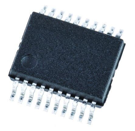
| 描述 | IC ADC 24BIT STEREO 20-SSOP音频模/数转换器 IC 24-Bit 96kHz Stereo D-S ADC |
| 产品分类 | |
| 品牌 | Texas Instruments |
| 产品手册 | |
| 产品图片 |
|
| rohs | 符合RoHS无铅 / 符合限制有害物质指令(RoHS)规范要求 |
| 产品系列 | 音频 IC,音频模/数转换器 IC,Texas Instruments PCM1803ADB- |
| 数据手册 | |
| 产品型号 | PCM1803ADB |
| 产品培训模块 | http://www.digikey.cn/PTM/IndividualPTM.page?site=cn&lang=zhs&ptm=13240 |
| 产品目录页面 | |
| 产品种类 | 音频模/数转换器 IC |
| 供应商器件封装 | 20-SSOP |
| 信噪比 | 103 dB |
| 其它名称 | 296-19473-5 |
| 分辨率 | 24 bit |
| 分辨率(位) | 24 b |
| 制造商产品页 | http://www.ti.com/general/docs/suppproductinfo.tsp?distId=10&orderablePartNumber=PCM1803ADB |
| 功耗 | 60 mW |
| 包装 | 管件 |
| 单位重量 | 190 mg |
| 商标 | Texas Instruments |
| 安装类型 | 表面贴装 |
| 安装风格 | SMD/SMT |
| 封装 | Tube |
| 封装/外壳 | 20-SSOP(0.209",5.30mm 宽) |
| 封装/箱体 | SSOP-20 |
| 工作温度 | -40°C ~ 85°C |
| 工作电源电压 | 5 V, 4.5 V |
| 工厂包装数量 | 65 |
| 数据接口 | 串行 |
| 最大功率耗散 | 80 mW |
| 最大工作温度 | + 85 C |
| 最小工作温度 | - 25 C |
| 标准包装 | 65 |
| 电压-电源 | 2.7 V ~ 3.6 V,4.5 V ~ 5.5 V |
| 电压源 | 模拟和数字 |
| 电源电压-最大 | 5.5 V |
| 电源电压-最小 | 4.5 V |
| 电源电流 | 11.7 mA |
| 类型 | ADC, 音频 |
| 系列 | PCM1803A |
| 转换器数量 | 2 |
| 转换速率 | 96 kS/s |
| 通道数量 | 2 Channel |
| 采样率(每秒) | 96k |


- 商务部:美国ITC正式对集成电路等产品启动337调查
- 曝三星4nm工艺存在良率问题 高通将骁龙8 Gen1或转产台积电
- 太阳诱电将投资9.5亿元在常州建新厂生产MLCC 预计2023年完工
- 英特尔发布欧洲新工厂建设计划 深化IDM 2.0 战略
- 台积电先进制程称霸业界 有大客户加持明年业绩稳了
- 达到5530亿美元!SIA预计今年全球半导体销售额将创下新高
- 英特尔拟将自动驾驶子公司Mobileye上市 估值或超500亿美元
- 三星加码芯片和SET,合并消费电子和移动部门,撤换高东真等 CEO
- 三星电子宣布重大人事变动 还合并消费电子和移动部门
- 海关总署:前11个月进口集成电路产品价值2.52万亿元 增长14.8%


PDF Datasheet 数据手册内容提取
Product Sample & Technical Tools & Support & Folder Buy Documents Software Community PCM1803A SLES142B–JUNE2005–REVISEDJULY2016 PCM1803A Single-Ended, Analog-Input 24-Bit, 96-kHz Stereo A/D Converter 1 Features 2 Applications • 24-BitDelta-SigmaStereoA/DConverter • AVAmplifierReceivers 1 • Single-EndedVoltageInput:3V • MDPlayers p-p • OversamplingDecimationFilter: • CDRecorders – OversamplingFrequency: ×64, ×128 • MultitrackReceivers – Pass-BandRipple:±0.05dB • ElectricMusicalInstruments – Stop-BandAttenuation: –65dB 3 Description – On-ChipHigh-PassFilter:0.84Hz(44.1kHz) The PCM1803A device is high-performance, low- • High-Performance: cost, single-chip stereo analog-to-digital converter – THD+N: –95dB(Typically) with single-ended analog voltage input. The – SNR:103dB(Typically) PCM1803A uses a delta-sigma modulator with 64- and 128-times oversampling, and includes a digital – DynamicRange:103dB(Typically) decimation filter and high-pass filter, which removes • PCMAudioInterface: the DC component of the input signal. For various – MasterorSlaveModeSelectable applications, the PCM1803A supports master and slave modes and four data formats in serial interface. – DataFormats: The PCM1803A is suitable for a wide variety of cost- – 24-BitLeft-Justified sensitive consumer applications where good – 24-BitI2S performance and operation from a 5-V analog supply and 3.3-V digital supply are required. The PCM1803A – 20-,24-BitRight-Justified is fabricated using a highly-advanced CMOS process • SamplingRate:16kHzto96kHz andisavailableinasmall20-pinSSOPpackage. • SystemClock:256f ,384f ,512f ,768f S S S S • DualPowerSupplies:5VforAnalog,3.3Vfor DeviceInformation(1) Digital PARTNUMBER PACKAGE BODYSIZE(NOM) • Package:20-PinSSOP PCM1803A SSOP(20) 7.20mm×5.30mm (1) For all available packages, see the orderable addendum at theendofthedatasheet. FunctionalBlockDiagram Delta-Sigma BCK VINL Modulator LRCK DOUT Serial ×1/64 ,×1/128 Interface VREF1 Decimation Reference Filter VREF2 With Mode/ High-Pass Filter Format FMT0 Control FMT1 Delta-Sigma MODE0 VINR Modulator MODE1 BYPAS TEST OSR Power Supply Clock and Timing Control PDWN SCKI VCC AGND DGND VDD B0004-06 Copyright © 2016,Texas Instruments Incorporated 1 An IMPORTANT NOTICE at the end of this data sheet addresses availability, warranty, changes, use in safety-critical applications, intellectualpropertymattersandotherimportantdisclaimers.PRODUCTIONDATA.
PCM1803A SLES142B–JUNE2005–REVISEDJULY2016 www.ti.com Table of Contents 1 Features.................................................................. 1 7.4 DeviceFunctionalModes........................................12 2 Applications........................................................... 1 8 ApplicationandImplementation........................ 17 3 Description............................................................. 1 8.1 ApplicationInformation............................................17 4 RevisionHistory..................................................... 2 8.2 TypicalApplication .................................................17 5 PinConfigurationandFunctions......................... 3 9 PowerSupplyRecommendations...................... 19 6 Specifications......................................................... 4 10 Layout................................................................... 19 6.1 AbsoluteMaximumRatings......................................4 10.1 LayoutGuidelines.................................................19 6.2 ESDRatings..............................................................4 10.2 LayoutExample....................................................20 6.3 RecommendedOperatingConditions.......................4 11 DeviceandDocumentationSupport................. 21 6.4 ThermalInformation..................................................5 11.1 ReceivingNotificationofDocumentationUpdates21 6.5 ElectricalCharacteristics...........................................5 11.2 CommunityResources..........................................21 6.6 TypicalCharacteristics..............................................7 11.3 Trademarks...........................................................21 7 DetailedDescription............................................ 10 11.4 ElectrostaticDischargeCaution............................21 7.1 Overview.................................................................10 11.5 Glossary................................................................21 7.2 FunctionalBlockDiagram.......................................10 12 Mechanical,Packaging,andOrderable Information........................................................... 21 7.3 FeatureDescription.................................................10 4 Revision History NOTE:Pagenumbersforpreviousrevisionsmaydifferfrompagenumbersinthecurrentversion. ChangesfromRevisionA(August2006)toRevisionB Page • AddedESDRatingstable,FeatureDescriptionsection,DeviceFunctionalModes,ApplicationandImplementation section,PowerSupplyRecommendationssection,Layoutsection,DeviceandDocumentationSupportsection,and Mechanical,Packaging,andOrderableInformationsection.................................................................................................. 1 • ChangedR valuefrom115°C/Wto84.4°C/WinThermalInformation............................................................................ 5 θJA • ChangedtheThermalInformationtable ................................................................................................................................ 5 2 SubmitDocumentationFeedback Copyright©2005–2016,TexasInstrumentsIncorporated ProductFolderLinks:PCM1803A
PCM1803A www.ti.com SLES142B–JUNE2005–REVISEDJULY2016 5 Pin Configuration and Functions DBPackage 20-PinSSOP TopView V L 1 20 MODE1 IN V R 2 19 MODE0 IN V 1 3 18 FMT1 REF V 2 4 17 FMT0 REF V 5 16 OSR CC AGND 6 15 SCKI PDWN 7 14 V DD BYPAS 8 13 DGND TEST 9 12 DOUT LRCK 10 11 BCK Not to scale PinFunctions PIN I/O DESCRIPTION NAME NO. AGND 6 – AnalogGND BCK 11 I/O Audiodatabitclockinput/output(1) BYPAS 8 I HPFbypasscontrol.LOW:Normalmode(DCreject);HIGH:Bypassmode(through)(2) DGND 13 – DigitalGND DOUT 12 O Audiodatadigitaloutput FMT0 17 I Audiodataformatselectinput0.SeeDataFormat.(2) FMT1 18 I Audiodataformatselectinput1.SeeDataFormat.(2) LRCK 10 I/O Audiodatalatchenableinput/output(1) MODE0 19 I Modeselectinput0.SeeDataFormat.(2) MODE1 20 I Modeselectinput1.SeeDataFormat.(2) OSR 16 I Oversamplingratioselectinput.LOW:×64f ,HIGH:×128f (2) S S PDWN 7 I Power-downcontrol,active-low (2) SCKI 15 I Systemclockinput:256f ,384f ,512f ,or768f (3) S S S S TEST 9 I Test,mustbeconnectedtoDGND(2) V 5 – Analogpowersupply,5-V CC V 14 – Digitalpowersupply,3.3-V DD V L 1 I Analoginput,L-channel IN V R 2 I Analoginput,R-channel IN V 1 3 – Reference-voltage-1decouplingcapacitor REF V 2 4 – Reference-voltage-2decouplingcapacitor REF (1) Schmitt-triggerinput (2) Schmitt-triggerinputwithinternalpulldown(50kΩ,typically),5-Vtolerant (3) Schmitt-triggerinput,5-Vtolerant Copyright©2005–2016,TexasInstrumentsIncorporated SubmitDocumentationFeedback 3 ProductFolderLinks:PCM1803A
PCM1803A SLES142B–JUNE2005–REVISEDJULY2016 www.ti.com 6 Specifications 6.1 Absolute Maximum Ratings overoperatingfree-airtemperaturerange(unlessotherwisenoted)(1) MIN MAX UNIT V –0.3 6.5 CC Supplyvoltage V V –0.3 4 DD Groundvoltagedifferences AGND,DGND ±0.1 V LRCK,BCK,DOUT –0.3 (V +0.3)<4 DD Digitalinputvoltage,VI PDWN,BYPAS,TEST,SCKI,OSR,FMT0,FMT1, V –0.3 6.5 MODE0,MODE1 Analoginputvoltage,V V L,V R,V 1,V 2 –0.3 (V +0.3)<6.5 V I IN IN REF REF CC Inputcurrent,I Anypinsexceptsupplies ±10 mA I Ambienttemperatureunderbias,T –40 125 °C bias Junctiontemperature,T 150 °C J Leadtemperature(soldering) 5s 260 °C Packagetemperature(IRreflow,peak) 260 °C Storagetemperature,T –55 150 °C stg (1) StressesbeyondthoselistedunderAbsoluteMaximumRatingsmaycausepermanentdamagetothedevice.Thesearestressratings only,whichdonotimplyfunctionaloperationofthedeviceattheseoranyotherconditionsbeyondthoseindicatedunderRecommended OperatingConditions.Exposuretoabsolute-maximum-ratedconditionsforextendedperiodsmayaffectdevicereliability. 6.2 ESD Ratings VALUE UNIT Electrostatic Human-bodymodel(HBM),perANSI/ESDA/JEDECJS-001(1) ±4000 V V (ESD) discharge Charged-devicemodel(CDM),perJEDECspecificationJESD22-C101(2) ±1500 (1) JEDECdocumentJEP155statesthat500-VHBMallowssafemanufacturingwithastandardESDcontrolprocess. (2) JEDECdocumentJEP157statesthat250-VCDMallowssafemanufacturingwithastandardESDcontrolprocess. 6.3 Recommended Operating Conditions overoperatingfree-airtemperaturerange MIN NOM MAX UNIT Analogsupplyvoltage,V 4.5 5 5.5 V CC Digitalsupplyvoltage,V 2.7 3.3 3.6 V DD Analoginputvoltage,full-scale(–0dB) 3 Vp-p Digitalinputlogicfamily TTL Systemclock 8.192 49.152 MHz Digitalinputclockfrequency Samplingclock 32 96 kHz Digitaloutputloadcapacitance 20 pF Operatingfree-airtemperature,T –25 85 °C A 4 SubmitDocumentationFeedback Copyright©2005–2016,TexasInstrumentsIncorporated ProductFolderLinks:PCM1803A
PCM1803A www.ti.com SLES142B–JUNE2005–REVISEDJULY2016 6.4 Thermal Information PCM1803A THERMALMETRIC(1) DB(SSOP) UNIT 20PINS R Junction-to-ambientthermalresistance 84.4 °C/W θJA R Junction-to-case(top)thermalresistance 42.4 °C/W θJC(top) R Junction-to-boardthermalresistance 41.4 °C/W θJB ψ Junction-to-topcharacterizationparameter 8.3 °C/W JT ψ Junction-to-boardcharacterizationparameter 40.7 °C/W JB R Junction-to-case(bottom)thermalresistance — °C/W θJC(bot) (1) Formoreinformationabouttraditionalandnewthermalmetrics,seetheSemiconductorandICPackageThermalMetricsapplication report. 6.5 Electrical Characteristics AllspecificationsatT =25°C,V =5V,V =3.3V,mastermode,f =44.1kHz,systemclock=384f , A CC DD S S oversamplingratio=×128,24-bitdata(unlessotherwisenoted) PARAMETER TESTCONDITIONS MIN TYP MAX UNIT Resolution 24 Bits DATAFORMAT Audiodatainterfaceformat Left-justified,I2S,right-justified Audiodatabitlength 20,24 Bits Audiodataformat MSB-first,2scomplement f Samplingfrequency 16 44.1 96 kHz S 256f 4.096 11.2896 24.576 S 384f 6.144 16.9344 36.864 S Systemclockfrequency MHz 512f 8.192 22.5792 49.152 S 768f 12.288 33.8688 S INPUTLOGIC V (1) 2 V IH DD V (1) 0 0.8 IL Inputlogic-levelvoltage Vdc V (2) (3) 2 5.5 IH V (2) (3) 0 0.8 IL I (1) (2) V =V ±10 IH IN DD I (1) (2) V =0 ±10 IL IN Inputlogic-levelcurrent μA I (3) V =V 65 100 IH IN DD I (3) V =0 ±10 IL IN OUTPUTLOGIC V (4) I =–4mA 2.8 OH OUT Outputlogic-levelvoltage Vdc V (4) I =4mA 0.5 OL OUT DCACCURACY Gainmismatch,channel-to-channel ±1 ±3 %ofFSR Gainerror ±2 ±4 %ofFSR Bipolarzeroerror HPFbypass ±0.4 %ofFSR (1) Pins10to11:LRCK,BCK(Schmitt-triggerinput,inslavemode) (2) Pin15:SCKI(Schmitt-triggerinput,5-Vtolerant) (3) Pins7to9,16to20:PDWN,BYPAS,TEST,OSR,FMT0,FMT1,MODE0,MODE1(Schmitt-triggerinput,with50-kΩtypicalpulldown resistor,5-Vtolerant) (4) Pins10to12:LRCK,BCK(inmastermode),DOUT Copyright©2005–2016,TexasInstrumentsIncorporated SubmitDocumentationFeedback 5 ProductFolderLinks:PCM1803A
PCM1803A SLES142B–JUNE2005–REVISEDJULY2016 www.ti.com Electrical Characteristics (continued) AllspecificationsatT =25°C,V =5V,V =3.3V,mastermode,f =44.1kHz,systemclock=384f , A CC DD S S oversamplingratio=×128,24-bitdata(unlessotherwisenoted) PARAMETER TESTCONDITIONS MIN TYP MAX UNIT DYNAMICPERFORMANCE(5) V =–0.5dB,f =44.1kHz –95 –89 IN S V =–0.5dB,f =96kHz(6) –93 IN S THD+N Totalharmonicdistortion+noise dB V =–60dB,f =44.1kHz –41 IN S V =–60dB,f =96kHz(6) –41 IN S f =44.1kHz,A-weighted 100 103 S Dynamicrange dB f =96kHz,A-weighted(6) 103 S f =44.1kHz,A-weighted 100 103 S SNR Signal-to-noiseratio dB f =96kHz,A-weighted(6) 103 S f =44.1kHz 95 98 S Channelseparation dB f =96kHz(6) 99 S ANALOGINPUT V Inputvoltage 0.6×V Vp-p I CC Centervoltage(V 1) 0.5×V V REF CC Inputimpedance 40 kΩ DIGITALFILTERPERFORMANCE Passband 0.454×f Hz S Stopband 0.583×f Hz S Pass-bandripple ±0.05 dB Stop-bandattenuation –65 dB t Groupdelaytime 17.4/f s GD S HPFfrequencyresponse –3dB 0.019×f mHz S POWERSUPPLYREQUIREMENTS V 4.5 5 5.5 Vdc CC Supplyvoltagerange V 2.7 3.3 3.6 Vdc DD 7.7 10 mA I CC Powerdown(8) 5 μA Supplycurrent(7) f =44.1kHz 6.5 9 mA S I f =96kHz(6) 11.7 mA DD S Powerdown(8) 1 μA f =44.1kHz 60 80 mW S Powerdissipation f =96kHz(6) 77 mW S Powerdown(8) 28 μW TEMPERATURERANGE T Operatingfree-airtemperature –40 85 °C A (5) AnalogperformancespecificationsaretestedusingtheSystemTwo™audiomeasurementsystembyAudioPrecision™,using400-Hz HPF,20-kHzLPFinrmsmode. (6) f =96kHz,systemclock=256f ,oversamplingratio=×64. S S (7) MinimumloadonDOUT(pin12),BCK(pin11),LRCK(pin10) (8) HaltSCKI,BCK,LRCK 6 SubmitDocumentationFeedback Copyright©2005–2016,TexasInstrumentsIncorporated ProductFolderLinks:PCM1803A
PCM1803A www.ti.com SLES142B–JUNE2005–REVISEDJULY2016 6.6 Typical Characteristics 6.6.1 TypicalCurvesofInternalFilter 6.6.1.1 DecimationFilterFrequencyResponse All specifications at T = 25°C, V = 5 V, V = 3.3 V, master mode, f = 44.1 kHz, system clock = 384 f , A CC DD S S oversamplingratio=×128,24-bitdata(unlessotherwisenoted) 50 50 Oversampling Ratio = (cid:1)128 Oversampling Ratio = (cid:1)64 0 0 B B d −50 d −50 de − de − u u mplit −100 mplit −100 A A −150 −150 −200 −200 0 8 16 24 32 40 48 56 64 0 8 16 24 32 Normalized Frequency [× fS] Normalized Frequency [× fS] G001 G002 Figure1.OverallCharacteristics Figure2.OverallCharacteristics 0 0.2 −10 0.0 −20 −30 −0.2 mplitude − dB −−−654000 mplitude − dB −0.4 A A −0.6 −70 −80 −0.8 −90 Oversampling Oversampling Ratio = (cid:1)128 and (cid:1)64 Ratio = (cid:1)128 and (cid:1)64 −100 −1.0 0.00 0.25 0.50 0.75 1.00 0.0 0.1 0.2 0.3 0.4 0.5 0.6 Normalized Frequency [× fS] G003 Normalized Frequency [× fS] G004 Figure3.Stop-BandAttenuationCharacteristics Figure4.Pass-BandRippleCharacteristics 6.6.1.2 Low-CutFilterFrequencyResponse AllspecificationsatT =25°C,V =5V,V =3.3V,mastermode,f =44.1kHz,systemclock=384f , A CC DD S S oversamplingratio=×128,24-bitdata(unlessotherwisenoted) 0 0.2 −10 0.0 −20 −30 −0.2 B B d −40 d ude − −50 ude − −0.4 mplit −60 mplit A A −0.6 −70 −80 −0.8 −90 −100 −1.0 0.0 0.1 0.2 0.3 0.4 0 1 2 3 4 Normalized Frequency [× fS/1000] Normalized Frequency [× fS/1000] G005 G006 Figure5.HPFStop-BandCharacteristics Figure6.HPFPass-BandCharacteristics Copyright©2005–2016,TexasInstrumentsIncorporated SubmitDocumentationFeedback 7 ProductFolderLinks:PCM1803A
PCM1803A SLES142B–JUNE2005–REVISEDJULY2016 www.ti.com 6.6.2 TypicalPerformanceCurves AllspecificationsatT =25°C,V =5V,V =3.3V,mastermode,f =44.1kHz,systemclock=384f , A CC DD S S oversamplingratio=×128,24-bitdata(unlessotherwisenoted) −90 110 B d − −91 109 e s Noi −92 B 108 on + −93 R − d 107 Distorti −94 and SN 106 monic −−9965 Range 110045 Dynamic Range − Total Har −−9987 Dynamic 110023 SNR N D+ −99 101 H T −100 100 −50 −25 0 25 50 75 100 −50 −25 0 25 50 75 100 TA − Free-Air Temperature − °C TA − Free-Air Temperature − °C G007 G008 Figure7.TotalHarmonicDistortion+Noisevs Figure8.DynamicRangeandSignal-to-NoiseRatiovs Temperature Temperature −90 110 B d − −91 109 e s Noi −92 B 108 on + −93 R − d 107 Distorti −94 and SN 106 monic −−9965 Range 110045 Dynamic Range − Total Har −−9987 Dynamic 110023 SNR N D+ −99 101 H T −100 100 4.25 4.50 4.75 5.00 5.25 5.50 5.75 4.25 4.50 4.75 5.00 5.25 5.50 5.75 VCC − Supply Voltage − V VCC − Supply Voltage − V G009 G010 Figure9.TotalHarmonicDistortion+NoisevsSupply Figure10.DynamicRangeandSignal-to-NoiseRatiovs Voltage SupplyVoltage −90 110 dB (1)fS = 48 kHz, System Clock = 256 fS, Noise − −−9921 B 110089 ( 2 )OOfSvv ee=rr 9ss6aa mmkHppzllii,nn Sggy RRsaatettiimoo ==C l××o16c24k8. =. 256 fS, on + −93 R − d 107 Distorti −94 and SN 106 monic −−9965 Range 110045 Dynamic Range N − Total Har −−9987 ( 1 )OfSv e=r 4s8a mkHpzli,n Sgy Rsatetimo =C l×o1c2k8 =. 256 fS, Dynamic 110023 SNR D+ −99 (2)fS = 96 kHz, System Clock = 256 fS, 101 H Oversampling Ratio = ×64. T −100 100 0 4140.1 4280(1) 9360(2) 40 0 4140.1 4280(1) 9360(2) 40 fSAMPLE Condition − kHz fSAMPLE Condition − kHz G011 G012 Figure11.TotalHarmonicDistortion+Noisevsf Figure12.DynamicRangeandSignal-to-NoiseRatiovs SAMPLE Condition f Condition SAMPLE 8 SubmitDocumentationFeedback Copyright©2005–2016,TexasInstrumentsIncorporated ProductFolderLinks:PCM1803A
PCM1803A www.ti.com SLES142B–JUNE2005–REVISEDJULY2016 6.6.3 OutputSpectrum 0 0 Input Level = −0.5 dB Input Level = −60 dB Data Points = 8192 Data Points = 8192 −20 −20 −40 −40 B B d d de − −60 de − −60 u u plit −80 plit −80 m m A A −100 −100 −120 −120 −140 −140 0 5 10 15 20 0 5 10 15 20 f − Frequency − kHz f − Frequency − kHz G013 G014 Figure13.OutputSpectrum Figure14.OutputSpectrum 0 B d − −10 e s oi −20 N + n −30 o orti −40 st Di c −50 ni o m −60 ar H al −70 ot − T −80 N D+ −90 H T −100 −100−90 −80 −70 −60 −50 −40 −30 −20 −10 0 Signal Level − dB G015 Figure15.TotalHarmonicDistortion+NoisevsSignalLevel 6.6.4 SupplyCurrent 15 A m nt − IDD e 10 urr C ply ICC p u S − D D 5 d I n a CC (1)fS = 48 kHz, System Clock = 256 fS, I Oversampling Ratio = ×128. (2)fS = 96 kHz, System Clock = 256 fS, Oversampling Ratio = ×64. 0 0 4140.1 4280(1) 9360(2) 40 fSAMPLE Condition − kHz G016 Figure16.SupplyCurrentvsf Condition SAMPLE Copyright©2005–2016,TexasInstrumentsIncorporated SubmitDocumentationFeedback 9 ProductFolderLinks:PCM1803A
PCM1803A SLES142B–JUNE2005–REVISEDJULY2016 www.ti.com 7 Detailed Description 7.1 Overview The PCM1803A is suitable for a wide variety of cost-sensitive consumer applications where good performance and operation from a 5-V analog supply and 3.3-V digital supply are required. With hardware control and straightforward operation, the PCM1803A can quickly be implemented into an application. The PCM1803A supportssamplingratesfrom16kHzto96kHzaswellasleftjustified,rightjustified,andI2Sformats,allowingits useinavarietyofaudiosystems. 7.2 Functional Block Diagram Delta-Sigma BCK VINL Modulator LRCK DOUT Serial ×1/64 ,×1/128 Interface VREF1 Decimation Reference Filter VREF2 With Mode/ High-Pass Filter Format FMT0 Control FMT1 Delta-Sigma MODE0 VINR Modulator MODE1 BYPAS TEST OSR Power Supply Clock and Timing Control PDWN SCKI VCC AGND DGND VDD B0004-06 Copyright © 2016,Texas Instruments Incorporated 7.3 Feature Description 7.3.1 HardwareControl Pins FMT0, FMT1, OSR, BYPASS, MD0, and MD1 allow the device to be controlled by either tying these pins to GND,orVDD,aswellasGPIO,fromahostIC.ThesecontrolsallowfullconfigurationofthePCM1803A. 7.3.2 Power-On-ResetSequence The PCM1803A has an internal power-on-reset circuit, and initialization (reset) is performed automatically at the time when power-supply voltage (V ) exceeds 2.2 V (typical). While V < 2.2 V (typical) and for 1024 system DD DD clock cycles after V > 2.2 V (typical), the PCM1803A stays in the reset state, and the digital output is forced to DD zero. The digital output becomes valid when a time period of 4480/f has elapsed following release from the S resetstate.Figure17illustratestheinternalpower-on-resettimingandthedigitaloutputforpower-onreset. 10 SubmitDocumentationFeedback Copyright©2005–2016,TexasInstrumentsIncorporated ProductFolderLinks:PCM1803A
PCM1803A www.ti.com SLES142B–JUNE2005–REVISEDJULY2016 Feature Description (continued) 2.6 V VDD 2.2 V 1.8 V Reset Reset Removal Internal Reset 1024 System Clocks 4480 / fS System Clock DOUT Zero Data Normal Data T0014-05 Figure17. InternalPower-On-ResetTiming 7.3.3 SystemClock The PCM1803A supports 256 f , 384 f , 512 f , and 768 f as the system clock, where f is the audio sampling S S S S S frequency.ThesystemclockmustbesuppliedonSCKI(pin15). The PCM1803A has a system clock-detection circuit that automatically senses if the system clock is operating at 256 f , 384 f , 512 f , or 768 f in slave mode. In master mode, the system clock frequency must be selected by S S S S MODE0 (pin 19) and MODE1 (pin 20), and 768 f is not available. The system clock is divided automatically into S 128f and64f ,andthesefrequenciesareusedtooperatethedigitalfilterandthedelta-sigmamodulator. S S Table 1 shows the relationship of typical sampling frequency and system clock frequency, and Figure 18 shows systemclocktiming. Table1.SamplingFrequencyandSystemClockFrequency SYSTEMCLOCKFREQUENCY(MHz) SAMPLINGFREQUENCY(kHz) 256f 384f 512f 768f (1) S S S S 32 8.1920 12.2880 16.3840 24.5760 44.1 11.2896 16.9344 22.5792 33.8688 48 12.2880 18.4320 24.5760 36.8640 64 16.3840 24.5760 32.7680 49.1520 88.2 22.5792 33.8688 45.1584 – 96 24.5760 36.8640 49.1520 – (1) Slavemodeonly tw(SCKH) tw(SCKL) SCKI 2 V SCKI 0.8 V T0005B07 Figure18. SystemClockTiming Copyright©2005–2016,TexasInstrumentsIncorporated SubmitDocumentationFeedback 11 ProductFolderLinks:PCM1803A
PCM1803A SLES142B–JUNE2005–REVISEDJULY2016 www.ti.com Table2.SystemClockTimingRequirements PARAMETER MIN MAX UNIT t Systemclockpulseduration,HIGH 8 ns w(SCKH) t Systemclockpulseduration,LOW 8 ns w(SCKL) Thequalityofthesystemclockcaninfluencethedynamicperformance,becausethePCM1803Aoperatesbased on a system clock. Therefore, it may be required to consider the system-clock duty, jitter, and the time difference betweensystem-clocktransitionandBCKorLRCKtransitionintheslavemode. 7.4 Device Functional Modes 7.4.1 SerialAudioDataInterface ThePCM1803AinterfacestheaudiosystemthroughBCK(pin11),LRCK(pin10),andDOUT(pin12). 7.4.1.1 InterfaceMode The PCM1803A supports master mode and slave mode as interface modes, and they are selected by MODE1 (pin20)andMODE0(pin19)asshowninTable3. In master mode, the PCM1803A provides the timing of serial audio data communications between the PCM1803A and the digital audio processor or external circuit. While in slave mode, the PCM1803A receives the timingfordatatransfersfromanexternalcontroller. Table3.InterfaceMode MODE1 MODE0 INTERFACEMODE 0 0 Slavemode(256f ,384f ,512f ,768f ) S S S S 0 1 Mastermode(512f ) S 1 0 Mastermode(384f ) S 1 1 Mastermode(256f ) S 7.4.1.1.1 MasterMode Inmastermode,BCKandLRCKworkasoutputpins,andthesepinsarecontrolledbytiming,whichisgenerated in the clock circuit of the PCM1803A. The frequency of BCK is fixed at LRCK × 64. The 768-f system clock is S notavailableinmastermode. 7.4.1.1.2 SlaveMode In slave mode, BCK and LRCK work as input pins. The PCM1803A accepts the 64-BCK/LRCK or 48-BCK/LRCK format(onlyfor384f and768f systemclocks),notthe32-BCK/LRCKformat. S S 7.4.1.2 DataFormat The PCM1803A supports four audio data formats in both master and slave modes, and the data formats are selectedbyFMT1(pin18)andFMT0(pin17)asshowninTable4.Figure19illustratesthedataformatsinslave andmastermodes. Table4.DataFormats FORMAT FMT1 FMT0 DESCRIPTION 0 0 0 Left-justified,24-bit 1 0 1 I2S,24-bit 2 1 0 Right-justified,24-bit 3 1 1 Right-justified,20-bit 12 SubmitDocumentationFeedback Copyright©2005–2016,TexasInstrumentsIncorporated ProductFolderLinks:PCM1803A
PCM1803A www.ti.com SLES142B–JUNE2005–REVISEDJULY2016 FORMAT 0: FMT[1:0] = 00 24-Bit, MSB-First, Left-Justified LRCK Left-Channel Right-Channel BCK DOUT 1 2 3 22 23 24 1 2 3 22 23 24 1 MSB LSB MSB LSB FORMAT 1: FMT[1:0] = 01 24-Bit, MSB-First, I2S LRCK Left-Channel Right-Channel BCK DOUT 1 2 3 22 23 24 1 2 3 22 23 24 MSB LSB MSB LSB FORMAT 2: FMT[1:0] = 10 24-Bit, MSB-First, Right-Justified LRCK Left-Channel Right-Channel BCK DOUT 24 1 2 3 22 23 24 1 2 3 22 23 24 MSB LSB MSB LSB FORMAT 3: FMT[1:0] = 11 20-Bit, MSB-First, Right-Justified LRCK Left-Channel Right-Channel BCK DOUT 20 1 2 3 18 19 20 1 2 3 18 19 20 MSB LSB MSB LSB T0016-11 Figure19. AudioDataFormats(LRCKandBCKWorkasInputsinSlaveModeandasOutputsinMaster Mode) 7.4.1.3 InterfaceTiming Figure 20 illustrates the interface timing in slave mode; Figure 21 and Figure 22 illustrate the interface timing in mastermode. Copyright©2005–2016,TexasInstrumentsIncorporated SubmitDocumentationFeedback 13 ProductFolderLinks:PCM1803A
PCM1803A SLES142B–JUNE2005–REVISEDJULY2016 www.ti.com t(LRCP) LRCK 1.4 V t(BCKL) t(LRSU) t(BCKH) t(LRHD) BCK 1.4 V t(BCKP) t(CKDO) t(LRDO) DOUT 0.5 VDD T0017-02 Figure20. AudioDataInterfaceTiming(SlaveMode:LRCKandBCKWorkasInputs) Table5.AudioDataInterfaceSlaveModeTimingRequirements(1) PARAMETER MIN TYP MAX UNIT t BCKperiod 1/(64f ) ns (BCKP) S t BCKpulseduration,HIGH 1.5×t ns (BCKH) (SCKI) t BCKpulseduration,LOW 1.5×t ns (BCKL) (SCKI) t LRCKsetuptimetoBCKrisingedge 40 ns (LRSU) t LRCKholdtimetoBCKrisingedge 20 ns (LRHD) t LRCKperiod 10 μs (LRCP) t Delaytime,BCKfallingedgetoDOUTvalid –10 40 ns (CKDO) t Delaytime,LRCKedgetoDOUTvalid –10 40 ns (LRDO) t Risingtimeofallsignals 20 ns r t Fallingtimeofallsignals 20 ns f (1) Timingmeasurementreferencelevelis1.4Vforinputand0.5V foroutput.Risingandfallingtimeismeasuredfrom10%to90%of DD IN/OUTsignalswing.LoadcapacitanceofDOUTis20pF.t meansSCKIperiodtime. (SCKI) t(LRCP) LRCK 0.5 VDD t(BCKL) t(BCKH) t(CKLR) BCK 0.5 VDD t(BCKP) t(CKDO) t(LRDO) DOUT 0.5 VDD T0018-02 Figure21. AudioDataInterfaceTiming(MasterMode:LRCKandBCKWorkasOutputs) 14 SubmitDocumentationFeedback Copyright©2005–2016,TexasInstrumentsIncorporated ProductFolderLinks:PCM1803A
PCM1803A www.ti.com SLES142B–JUNE2005–REVISEDJULY2016 Table6.AudioDataInterfaceMasterModeTimingRequirements(1) PARAMETER MIN TYP MAX UNIT t BCKperiod 150 1/(64f ) 1000 ns (BCKP) S t BCKpulseduration,HIGH 65 600 ns (BCKH) t BCKpulseduration,LOW 65 600 ns (BCKL) t Delaytime,BCKfallingedgetoLRCKvalid –10 20 ns (CKLR) t LRCKperiod 10 1/f 65 μs (LRCP) S t Delaytime,BCKfallingedgetoDOUTvalid –10 20 ns (CKDO) t Delaytime,LRCKedgetoDOUTvalid –10 20 ns (LRDO) t Risingtimeofallsignals 20 ns r t Fallingtimeofallsignals 20 ns f (1) Timingmeasurementreferencelevelis1.4Vforinputand0.5V foroutput.Risingandfallingtimeismeasuredfrom10%to90%of DD IN/OUTsignalswing.Loadcapacitanceofallsignalsis20pF. SCKI 1.4 V t(SCKBCK) t(SCKBCK) BCK 0.5 VDD T0074-01 Figure22. AudioClockInterfaceTiming(MasterMode:BCKWorksasOutput) Table7.AudioDataInterfaceMasterModeBCKTimingRequirements(1) PARAMETER MIN TYP MAX UNIT t Delaytime,SCKIrisingedgetoBCKedge 5 30 ns (SCKBCK) (1) Timingmeasurementreferencelevelis1.4Vforinputand0.5V foroutput.LoadcapacitanceofBCKis20pF. DD 7.4.2 SynchronizationWithDigitalAudioSystem In slave mode, the PCM1803A operates under LRCK, synchronized with system clock SCKI. The PCM1803A does not need a specific phase relationship between LRCK and SCKI, but does require the synchronization of LRCKandSCKI. If the relationship between LRCK and SCKI changes more than ±6 BCKs for 64 BCK/frame (±5 BCKs for 48 BCK/frame) during one sample period due to LRCK or SCKI jitter, internal operation of the ADC halts within 1/f , S anddigitaloutputisforcedtozerodata(BPZcode)untilresynchronizationbetweenLRCKandSCKIoccurs. In case of changes less than ±5 BCKs for 64 BCK/frame (±4 BCKs for 48 BCK/frame), resynchronization does notoccurandthepreviouslyexplaineddigitaloutputcontrolanddiscontinuitydonotoccur. Figure 23 illustrates the digital output response for loss of synchronization and resynchronization. During undefined data, the PCM1803A can generate some noise in the audio signal. Also, the transition of normal to undefined data and undefined or zero data to normal creates a discontinuity in the data of the digital output, whichcangeneratesomenoiseintheaudiosignal. Copyright©2005–2016,TexasInstrumentsIncorporated SubmitDocumentationFeedback 15 ProductFolderLinks:PCM1803A
PCM1803A SLES142B–JUNE2005–REVISEDJULY2016 www.ti.com Synchronization Lost Resynchronization State of Synchronization SYNCHRONOUS ASYNCHRONOUS SYNCHRONOUS 1/fS 32/fS UNDEFINED DOUT NORMAL DATA ZERO DATA NORMAL DATA DATA T0020-05 Figure23. ADCDigitalOutputforLossofSynchronizationandResynchronization 7.4.3 PowerDown PDWN (pin 7) controls operation of the entire ADC. During power-down mode, supply current for the analog portion is shut down and the digital portion is reset; also, DOUT (pin 12) is disabled. It is acceptable to halt the system clock during power-down mode so that power dissipation is minimized. The minimum LOW pulse durationonthePDWNpinis100ns. TI recommends setting PWDN (pin 7) to LOW once to obtain stable analog performance when the sampling rate, interfacemode,dataformat,oroversamplingcontrolischanged. Table8.Power-DownControl PWDN POWER-DOWNMODE LOW Power-downmode HIGH Normaloperationmode 7.4.4 HPFBypass Thebuilt-infunctionforDC-componentrejectioncanbebypassedbyBYPAS(pin8)control.Inbypassmode,the DC component of the input analog signal, internal DC offset, and so forth, also are converted and included in the digitaloutputdata. Table9.HPFBypassControl BYPAS HPF(HIGH-PASSFILTER)MODE LOW Normal(noDCcomponentinDOUT)mode HIGH Bypass(DCcomponentinDOUT)mode 7.4.5 OversamplingRatioControl OSR (pin 16) controls the oversampling ratio of the delta-sigma modulator, ×64 or ×128. The ×128 mode is availableforf ≤48kHz. S Table10.OversamplingControl OSR OVERSAMPLINGRATIO LOW ×64 HIGH ×128(f ≤48kHz) S 16 SubmitDocumentationFeedback Copyright©2005–2016,TexasInstrumentsIncorporated ProductFolderLinks:PCM1803A
PCM1803A www.ti.com SLES142B–JUNE2005–REVISEDJULY2016 8 Application and Implementation NOTE Information in the following applications sections is not part of the TI component specification, and TI does not warrant its accuracy or completeness. TI’s customers are responsible for determining suitability of components for their purposes. Customers should validateandtesttheirdesignimplementationtoconfirmsystemfunctionality. 8.1 Application Information The PCM1803A device is suitable for wide variety of cost-sensitive consumer applications requiring good performanceandoperationwitha5-Vanalogsupplyand3.3-Vdigitalsupply. 8.2 Typical Application Figure 24 illustrates a typical circuit connection diagram where the cutoff frequency of the input HPF is about 160kHz. C1 + R1 L-Ch IN 1 VINL MODE1 20 C2 + R2 Mode [1:0] R-Ch IN 2 VINR MODE0 19 C7 C8 C5 + 3 VREF1 FMT1 18 Control C6 + Format [1:0] 4 VREF2 FMT0 17 +5 V + 5 VCC OSR 16 Oversampling C4 PCM1803A 6 AGND SCKI 15 System Clock Power Down 7 PDWN VDD 14 + +3.3 V Control C3 LCF Bypass 8 BYPAS DGND 13 9 TEST DOUT 12 Data Out 10 LRCK BCK 11 Data Clock Audio Data Processor L/R Clock Copyright © 2016,Texas Instruments Incorporated A. C , C : A 1-μF electrolytic capacitor gives a 4-Hz (τ = 1 μF × 40 kΩ) cutoff frequency for the input HPF in normal 1 2 operationandrequiresapower-onsettlingtimewitha40-mstimeconstantduringthepower-oninitializationperiod. B. C ,C :Bypasscapacitorsare0.1-μFceramicand10-μFelectrolytic,dependingonlayoutandpowersupply. 3 4 C. C ,C :Recommendedcapacitorsare0.1-μFceramicand10-μFelectrolytic. 5 6 D. C , C , R , R : A 0.01-μF film-type capacitor and 100-Ω resistor give a 160-kHz (τ = 0.01 μF × 100 Ω) cutoff 7 8 1 2 frequencyfortheanti-aliasingfilterinnormaloperation. Figure24. TypicalApplicationDiagram Copyright©2005–2016,TexasInstrumentsIncorporated SubmitDocumentationFeedback 17 ProductFolderLinks:PCM1803A
PCM1803A SLES142B–JUNE2005–REVISEDJULY2016 www.ti.com Typical Application (continued) 8.2.1 DesignRequirements Forthisdesignexample,usetheparameterslistedinTable11 astheinputparameters. Table11.DesignParameters DESIGNPARAMETER EXAMPLEVALUE AnalogInputVoltageRange 0V to3V p-p p-p Output PCMaudiodata SystemClockInputFrequency 2.048MHzto49.152MHz OutputSamplingFrequency 8kHzto96kHz PowerSupply 3.3Vand5V 8.2.2 DetailedDesignProcedure 8.2.2.1 ControlPins The control pins such as the FMT, MODE, OSR, and BYPASS can be controlled by tying up to VDD, down to GND,ordrivenwithGPIOfromtheDSPoraudioprocessor. 8.2.2.2 DSPorAudioProcessor In this application a DSP or audio processor is acting as the audio master, and the PCM1803A is acting as the audio slave. This means the DSP or audio processor must be able to output audio clocks that the PCM1803A canusetoprocessaudiosignals. 8.2.2.3 InputFilters For the analog input circuit an AC coupling capacitor must be placed in series with the input. This removes the DC component of the input signal. An RC filter can also be implemented to filter out of band noise to reduce aliasing.Equation1canbeusedtocalculatethecutofffrequencyoftheoptionalRCfilterfortheinput. 1 f = c 2pRC (1) 8.2.3 ApplicationCurve −90 B d − −91 e s oi −92 N + n −93 o orti −94 st Di c −95 ni o m −96 ar H al −97 ot N − T −98 ( 1 )OfSv e=r 4s8a mkHpzli,n Sgy Rsatetimo =C l×o1c2k8 =. 256 fS, D+ −99 (2)fS = 96 kHz, System Clock = 256 fS, H Oversampling Ratio = ×64. T −100 0 4140.1 4280(1) 9360(2) 40 fSAMPLE Condition − kHz G011 Figure25. TotalHarmonicDistortion+Noisevsf Condition SAMPLE 18 SubmitDocumentationFeedback Copyright©2005–2016,TexasInstrumentsIncorporated ProductFolderLinks:PCM1803A
PCM1803A www.ti.com SLES142B–JUNE2005–REVISEDJULY2016 9 Power Supply Recommendations The PCM1803A requires a 5-V nominal supply and a 3.3-V nominal supply. The 5-V supply is for the analog circuitry powered by the VCC pin. The 3.3-V supply is for the digital circuitry powered by the VDD pin. The decouplingcapacitorsforthepowersuppliesmustbeplacedclosetothedeviceterminals. 10 Layout 10.1 Layout Guidelines 10.1.1 V ,V Pins CC DD The digital and analog power-supply lines to the PCM1803A must be bypassed to the corresponding ground pins with 0.1-μF ceramic and 10-μF electrolytic capacitors, as close to the pins as possible, to maximize the dynamic performanceoftheADC. 10.1.2 AGND,DGNDPins To maximize the dynamic performance of the PCM1803A, the analog and digital grounds are not connected internally. These grounds must have low impedance to avoid digital noise feeding back into the analog ground. Therefore,theymustbeconnecteddirectlytoeachotherundertheparttoreducepotentialnoiseproblems. 10.1.3 V L,V RPins IN IN The V L and V R pins need a simple external RC filter (f = 160 kHz) as an antialiasing filter to remove out-of- IN IN C band noise from the audio band. If the input signal includes noise with a frequency near the oversampling frequency (64 f or 128 f ), the noise is folded into the baseband (audio band) signal through A-to-D conversion. S S The recommended R value is 100 Ω. Film-type capacitors of 0.01 μF must be placed as close as possible to the V L and V R pins and must be terminated to GND as close as possible to the AGND pin to maximize the IN IN dynamicperformanceofADC,bysuppressingkickbacknoisefromthePCM1803A. 10.1.4 V 1Pin REF TI recommends a 0.1-μF ceramic capacitor and 10-μF electrolytic capacitor between V 1 and AGND to ensure REF low source impedance of the ADC references. These capacitors must be placed as close as possible to the V 1pintoreducedynamicerrorsontheADCreference. REF 10.1.5 V 2Pin REF The differential voltage between V 2 and AGND sets the analog input full-scale range. A 0.1-μF ceramic REF capacitor and 10-μF electrolytic capacitor are recommended between V 2 and AGND. These capacitors must REF beplacedascloseaspossibletotheV 2pintoreducedynamicerrorsontheADCreference. REF 10.1.6 DOUTPin The DOUT pin has enough load drive capability, but if the DOUT line is long, placing a buffer near the PCM1803A and minimizing load capacitance is recommended to minimize the digital-analog crosstalk and maximizethedynamicperformanceoftheADC. Copyright©2005–2016,TexasInstrumentsIncorporated SubmitDocumentationFeedback 19 ProductFolderLinks:PCM1803A
PCM1803A SLES142B–JUNE2005–REVISEDJULY2016 www.ti.com 10.2 Layout Example It is recommended to place a top layer ground pour for shielding around PCM1803A and connect to lower main PCB ground plane by multiple vias Option External RC antialiasing circuit 1 (cid:29)F R-ch IN + L-ch IN 1 VINL MODE1 20 + 1 (cid:29)F Make sure to have 2 VINR MODE0 19 ground pour separating + chantnheel Ltreaftc easn tdo R higehlpt 3 VREF1 FMT1 18 Control prevent crosstalk Bypass Capacitors are + 0.1 uF and 10 uF 4 VREF2 PCM1803A FMT0 17 Mgroakuen dsu proeu tro s heapvaera ting the clock signals from 5V 5 VCC OSR 16 surrounding traces + 10 (cid:29)F 0.1 (cid:29)F 6 AGND SCKI 15 7 PDWN VDD 14 3.3V Control + 8 BYPAS DGND 13 0.1 (cid:29)F 10 (cid:29)F Clock signals to DSP or Audio 9 TEST DOUT 12 Processor 10 LRCK BCK 11 Top Layer Ground Pour Via to bottom Ground Plane Top Layer Signal Traces Pad to top layer ground pour Figure26. LayoutRecommendation 20 SubmitDocumentationFeedback Copyright©2005–2016,TexasInstrumentsIncorporated ProductFolderLinks:PCM1803A
PCM1803A www.ti.com SLES142B–JUNE2005–REVISEDJULY2016 11 Device and Documentation Support 11.1 Receiving Notification of Documentation Updates To receive notification of documentation updates, navigate to the device product folder on ti.com. In the upper right corner, click on Alert me to register and receive a weekly digest of any product information that has changed.Forchangedetails,reviewtherevisionhistoryincludedinanyreviseddocument. 11.2 Community Resources The following links connect to TI community resources. Linked contents are provided "AS IS" by the respective contributors. They do not constitute TI specifications and do not necessarily reflect TI's views; see TI's Terms of Use. TIE2E™OnlineCommunity TI'sEngineer-to-Engineer(E2E)Community.Createdtofostercollaboration amongengineers.Ate2e.ti.com,youcanaskquestions,shareknowledge,exploreideasandhelp solveproblemswithfellowengineers. DesignSupport TI'sDesignSupport QuicklyfindhelpfulE2Eforumsalongwithdesignsupporttoolsand contactinformationfortechnicalsupport. 11.3 Trademarks E2EisatrademarkofTexasInstruments. SystemTwo,AudioPrecisionaretrademarksofAudioPrecision,Inc. Allothertrademarksarethepropertyoftheirrespectiveowners. 11.4 Electrostatic Discharge Caution Thesedeviceshavelimitedbuilt-inESDprotection.Theleadsshouldbeshortedtogetherorthedeviceplacedinconductivefoam duringstorageorhandlingtopreventelectrostaticdamagetotheMOSgates. 11.5 Glossary SLYZ022—TIGlossary. Thisglossarylistsandexplainsterms,acronyms,anddefinitions. 12 Mechanical, Packaging, and Orderable Information The following pages include mechanical, packaging, and orderable information. This information is the most current data available for the designated devices. This data is subject to change without notice and revision of thisdocument.Forbrowser-basedversionsofthisdatasheet,refertotheleft-handnavigation. Copyright©2005–2016,TexasInstrumentsIncorporated SubmitDocumentationFeedback 21 ProductFolderLinks:PCM1803A
PACKAGE OPTION ADDENDUM www.ti.com 6-Feb-2020 PACKAGING INFORMATION Orderable Device Status Package Type Package Pins Package Eco Plan Lead/Ball Finish MSL Peak Temp Op Temp (°C) Device Marking Samples (1) Drawing Qty (2) (6) (3) (4/5) PCM1803ADB ACTIVE SSOP DB 20 65 Green (RoHS NIPDAU Level-1-260C-UNLIM -40 to 85 PCM1803A & no Sb/Br) PCM1803ADBG4 ACTIVE SSOP DB 20 65 Green (RoHS NIPDAU Level-1-260C-UNLIM -40 to 85 PCM1803A & no Sb/Br) PCM1803ADBR ACTIVE SSOP DB 20 2000 Green (RoHS NIPDAU Level-1-260C-UNLIM -40 to 85 PCM1803A & no Sb/Br) PCM1803ADBRG4 ACTIVE SSOP DB 20 2000 Green (RoHS NIPDAU Level-1-260C-UNLIM -40 to 85 PCM1803A & no Sb/Br) (1) The marketing status values are defined as follows: ACTIVE: Product device recommended for new designs. LIFEBUY: TI has announced that the device will be discontinued, and a lifetime-buy period is in effect. NRND: Not recommended for new designs. Device is in production to support existing customers, but TI does not recommend using this part in a new design. PREVIEW: Device has been announced but is not in production. Samples may or may not be available. OBSOLETE: TI has discontinued the production of the device. (2) RoHS: TI defines "RoHS" to mean semiconductor products that are compliant with the current EU RoHS requirements for all 10 RoHS substances, including the requirement that RoHS substance do not exceed 0.1% by weight in homogeneous materials. Where designed to be soldered at high temperatures, "RoHS" products are suitable for use in specified lead-free processes. TI may reference these types of products as "Pb-Free". RoHS Exempt: TI defines "RoHS Exempt" to mean products that contain lead but are compliant with EU RoHS pursuant to a specific EU RoHS exemption. Green: TI defines "Green" to mean the content of Chlorine (Cl) and Bromine (Br) based flame retardants meet JS709B low halogen requirements of <=1000ppm threshold. Antimony trioxide based flame retardants must also meet the <=1000ppm threshold requirement. (3) MSL, Peak Temp. - The Moisture Sensitivity Level rating according to the JEDEC industry standard classifications, and peak solder temperature. (4) There may be additional marking, which relates to the logo, the lot trace code information, or the environmental category on the device. (5) Multiple Device Markings will be inside parentheses. Only one Device Marking contained in parentheses and separated by a "~" will appear on a device. If a line is indented then it is a continuation of the previous line and the two combined represent the entire Device Marking for that device. (6) Lead/Ball Finish - Orderable Devices may have multiple material finish options. Finish options are separated by a vertical ruled line. Lead/Ball Finish values may wrap to two lines if the finish value exceeds the maximum column width. Important Information and Disclaimer:The information provided on this page represents TI's knowledge and belief as of the date that it is provided. TI bases its knowledge and belief on information provided by third parties, and makes no representation or warranty as to the accuracy of such information. Efforts are underway to better integrate information from third parties. TI has taken and Addendum-Page 1
PACKAGE OPTION ADDENDUM www.ti.com 6-Feb-2020 continues to take reasonable steps to provide representative and accurate information but may not have conducted destructive testing or chemical analysis on incoming materials and chemicals. TI and TI suppliers consider certain information to be proprietary, and thus CAS numbers and other limited information may not be available for release. In no event shall TI's liability arising out of such information exceed the total purchase price of the TI part(s) at issue in this document sold by TI to Customer on an annual basis. Addendum-Page 2
PACKAGE MATERIALS INFORMATION www.ti.com 16-Jul-2016 TAPE AND REEL INFORMATION *Alldimensionsarenominal Device Package Package Pins SPQ Reel Reel A0 B0 K0 P1 W Pin1 Type Drawing Diameter Width (mm) (mm) (mm) (mm) (mm) Quadrant (mm) W1(mm) PCM1803ADBR SSOP DB 20 2000 330.0 16.4 8.2 7.5 2.5 12.0 16.0 Q1 PCM1803ADBR SSOP DB 20 2000 330.0 17.4 8.5 7.6 2.4 12.0 16.0 Q1 PackMaterials-Page1
PACKAGE MATERIALS INFORMATION www.ti.com 16-Jul-2016 *Alldimensionsarenominal Device PackageType PackageDrawing Pins SPQ Length(mm) Width(mm) Height(mm) PCM1803ADBR SSOP DB 20 2000 367.0 367.0 38.0 PCM1803ADBR SSOP DB 20 2000 336.6 336.6 28.6 PackMaterials-Page2
PACKAGE OUTLINE DB0020A SSOP - 2 mm max height SCALE 2.000 SMALL OUTLINE PACKAGE C 8.2 TYP 7.4 A 0.1 C PIN 1 INDEX AREA SEATING PLANE 18X 0.65 20 1 2X 7.5 5.85 6.9 NOTE 3 10 11 0.38 20X 0.22 5.6 B 0.1 C A B 5.0 NOTE 4 2 MAX (0.15) TYP 0.25 SEE DETAIL A GAGE PLANE 0 -8 0.95 0.05 MIN 0.55 DETA 15AIL A TYPICAL 4214851/B 08/2019 NOTES: 1. All linear dimensions are in millimeters. Any dimensions in parenthesis are for reference only. Dimensioning and tolerancing per ASME Y14.5M. 2. This drawing is subject to change without notice. 3. This dimension does not include mold flash, protrusions, or gate burrs. Mold flash, protrusions, or gate burrs shall not exceed 0.15 mm per side. 4. This dimension does not include interlead flash. Interlead flash shall not exceed 0.25 mm per side. 5. Reference JEDEC registration MO-150. www.ti.com
EXAMPLE BOARD LAYOUT DB0020A SSOP - 2 mm max height SMALL OUTLINE PACKAGE 20X (1.85) SYMM (R0.05) TYP 1 20X (0.45) 20 SYMM 18X (0.65) 10 11 (7) LAND PATTERN EXAMPLE EXPOSED METAL SHOWN SCALE: 10X SOLDER MASK METAL METAL UNDER SOLDER MASK OPENING SOLDER MASK OPENING EXPOSED METAL EXPOSED METAL 0.07 MAX 0.07 MIN ALL AROUND ALL AROUND NON-SOLDER MASK SOLDER MASK DEFINED DEFINED (PREFERRED) SOLDE15.000 R MASK DETAILS 4214851/B 08/2019 NOTES: (continued) 6. Publication IPC-7351 may have alternate designs. 7. Solder mask tolerances between and around signal pads can vary based on board fabrication site. www.ti.com
EXAMPLE STENCIL DESIGN DB0020A SSOP - 2 mm max height SMALL OUTLINE PACKAGE 20X (1.85) SYMM (R0.05) TYP 1 20X (0.45) 20 SYMM 18X (0.65) 10 11 (7) SOLDER PASTE EXAMPLE BASED ON 0.125 mm THICK STENCIL SCALE: 10X 4214851/B 08/2019 NOTES: (continued) 8. Laser cutting apertures with trapezoidal walls and rounded corners may offer better paste release. IPC-7525 may have alternate design recommendations. 9. Board assembly site may have different recommendations for stencil design. www.ti.com
IMPORTANTNOTICEANDDISCLAIMER TI PROVIDES TECHNICAL AND RELIABILITY DATA (INCLUDING DATASHEETS), DESIGN RESOURCES (INCLUDING REFERENCE DESIGNS), APPLICATION OR OTHER DESIGN ADVICE, WEB TOOLS, SAFETY INFORMATION, AND OTHER RESOURCES “AS IS” AND WITH ALL FAULTS, AND DISCLAIMS ALL WARRANTIES, EXPRESS AND IMPLIED, INCLUDING WITHOUT LIMITATION ANY IMPLIED WARRANTIES OF MERCHANTABILITY, FITNESS FOR A PARTICULAR PURPOSE OR NON-INFRINGEMENT OF THIRD PARTY INTELLECTUAL PROPERTY RIGHTS. These resources are intended for skilled developers designing with TI products. You are solely responsible for (1) selecting the appropriate TI products for your application, (2) designing, validating and testing your application, and (3) ensuring your application meets applicable standards, and any other safety, security, or other requirements. These resources are subject to change without notice. TI grants you permission to use these resources only for development of an application that uses the TI products described in the resource. Other reproduction and display of these resources is prohibited. No license is granted to any other TI intellectual property right or to any third party intellectual property right. TI disclaims responsibility for, and you will fully indemnify TI and its representatives against, any claims, damages, costs, losses, and liabilities arising out of your use of these resources. TI’s products are provided subject to TI’s Terms of Sale (www.ti.com/legal/termsofsale.html) or other applicable terms available either on ti.com or provided in conjunction with such TI products. TI’s provision of these resources does not expand or otherwise alter TI’s applicable warranties or warranty disclaimers for TI products. Mailing Address: Texas Instruments, Post Office Box 655303, Dallas, Texas 75265 Copyright © 2020, Texas Instruments Incorporated