ICGOO在线商城 > 集成电路(IC) > 数据采集 - ADCs/DAC - 专用型 > PCM1770PW
 Datasheet下载
- 型号: PCM1770PW
- 制造商: Texas Instruments
- 库位|库存: xxxx|xxxx
- 要求:
| 数量阶梯 | 香港交货 | 国内含税 |
| +xxxx | $xxxx | ¥xxxx |
查看当月历史价格
查看今年历史价格
PCM1770PW产品简介:
ICGOO电子元器件商城为您提供PCM1770PW由Texas Instruments设计生产,在icgoo商城现货销售,并且可以通过原厂、代理商等渠道进行代购。 PCM1770PW价格参考¥14.75-¥30.09。Texas InstrumentsPCM1770PW封装/规格:数据采集 - ADCs/DAC - 专用型, DAC,音频 24 b 50k I²S 16-TSSOP。您可以下载PCM1770PW参考资料、Datasheet数据手册功能说明书,资料中有PCM1770PW 详细功能的应用电路图电压和使用方法及教程。
PCM1770PW是由Texas Instruments(德州仪器)生产的一款专用型数据采集ADC/DAC芯片,主要用于音频处理领域。该芯片集成了高性能的数模转换器(DAC),能够提供高质量的音频输出,适用于多种消费电子和专业音频设备。

 应用场景:

1. 音响系统:
   PCM1770PW广泛应用于家庭影院、立体声音响系统以及便携式音响设备中。它能够将数字音频信号转换为模拟信号,确保音质清晰、失真低,为用户提供高保真的听觉体验。

2. 汽车音响:
   在车载娱乐系统中,PCM1770PW可以用于提升车内音频播放的质量。其优异的信噪比和动态范围使得即使在嘈杂的环境中,也能保证音乐的纯净度和细节表现。

3. 便携式音频设备:
   例如MP3播放器、便携式CD机等设备中,PCM1770PW可以帮助实现更优质的音频输出。它的小尺寸封装使其适合集成到紧凑的设计中,同时保持出色的音频性能。

4. 专业音频设备:
   如录音棚中的监听设备、混音台等,PCM1770PW能够提供精确的音频还原能力,满足专业音频工程师对音质的苛刻要求。它的低失真特性有助于捕捉和再现细微的声音变化。

5. 语音通信设备:
   在电话会议系统、VoIP设备以及其他语音通信终端中,PCM1770PW可以改善通话质量,减少背景噪音干扰,提高语音清晰度,确保沟通顺畅。

6. 智能家居与物联网设备:
   随着智能音箱和其他具备语音交互功能的IoT设备的普及,PCM1770PW的应用也逐渐扩展到这些领域。它不仅提升了音频输出效果,还能支持多声道音频处理,增强用户体验。

总之,PCM1770PW凭借其卓越的音频处理能力和广泛的适用性,在各类需要高质量音频输出的设备中发挥着重要作用。
| 参数 | 数值 |
| 产品目录 | 集成电路 (IC)半导体 |
| DAC输出端数量 | 2 |
| 描述 | IC 24BIT LP STEREO DAC 16-TSSOP音频数/模转换器 IC 24-Bit Lo-Pwr Stereo DAC w/Headphone Amp |
| DevelopmentKit | DEM-DAI1770 |
| 产品分类 | |
| 品牌 | Texas Instruments |
| 产品手册 | http://www.ti.com/litv/sles011e |
| 产品图片 |
|
| rohs | 符合RoHS无铅 / 符合限制有害物质指令(RoHS)规范要求 |
| 产品系列 | 音频 IC,音频数/模转换器 IC,Texas Instruments PCM1770PW- |
| 数据手册 | |
| 产品型号 | PCM1770PW |
| PCN设计/规格 | |
| 产品培训模块 | http://www.digikey.cn/PTM/IndividualPTM.page?site=cn&lang=zhs&ptm=13240 |
| 产品目录页面 | |
| 产品种类 | 音频数/模转换器 IC |
| 位数 | 24 |
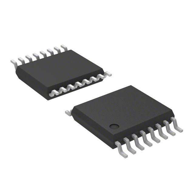
| 供应商器件封装 | 16-TSSOP |
| 信噪比 | 98 dB |
| 其它名称 | 296-13470-5 |
| 分辨率 | 24 bit |
| 制造商产品页 | http://www.ti.com/general/docs/suppproductinfo.tsp?distId=10&orderablePartNumber=PCM1770PW |
| 包装 | 管件 |
| 单位重量 | 63.100 mg |
| 商标 | Texas Instruments |
| 安装类型 | 表面贴装 |
| 安装风格 | SMD/SMT |
| 封装 | Tray |
| 封装/外壳 | 16-TSSOP(0.173",4.40mm 宽) |
| 封装/箱体 | TSSOP-16 |
| 工作温度 | -25°C ~ 85°C |
| 工作温度范围 | - 25 C to + 85 C |
| 工作电源电压 | 2.4 V |
| 工厂包装数量 | 250 |
| 建立时间 | - |
| 接口类型 | Serial (3-Wire) |
| 数据接口 | 并联 |
| 标准包装 | 250 |
| 电压源 | 单电源 |
| 系列 | PCM1770 |
| 转换器数 | 2 |
| 转换器数量 | 2 |
| 转换速率 | 48 kS/s |
| 输出数和类型 | 2 电压,单极 |
| 通道数量 | 2 Channel |
| 配用 | /product-detail/zh/DEM-DAI1770/DEM-DAI1770-ND/1898335/product-detail/zh/DEM-DAI1771/296-30900-ND/1898336 |
| 采样率(每秒) | 48k |


- 商务部:美国ITC正式对集成电路等产品启动337调查
- 曝三星4nm工艺存在良率问题 高通将骁龙8 Gen1或转产台积电
- 太阳诱电将投资9.5亿元在常州建新厂生产MLCC 预计2023年完工
- 英特尔发布欧洲新工厂建设计划 深化IDM 2.0 战略
- 台积电先进制程称霸业界 有大客户加持明年业绩稳了
- 达到5530亿美元!SIA预计今年全球半导体销售额将创下新高
- 英特尔拟将自动驾驶子公司Mobileye上市 估值或超500亿美元
- 三星加码芯片和SET,合并消费电子和移动部门,撤换高东真等 CEO
- 三星电子宣布重大人事变动 还合并消费电子和移动部门
- 海关总署:前11个月进口集成电路产品价值2.52万亿元 增长14.8%


PDF Datasheet 数据手册内容提取
(cid:2)(cid:17)(cid:14)(cid:14)(cid:20)(cid:2)(cid:14)(cid:13)(cid:18)(cid:12) (cid:4)(cid:14)(cid:13)(cid:8)(cid:17)(cid:7)(cid:16)(cid:15) (cid:10)(cid:14)(cid:13)(cid:11) (cid:5)(cid:9)(cid:19)(cid:6)(cid:15) (cid:3)(cid:12)(cid:15)(cid:16)(cid:14)(cid:17)(cid:11)(cid:9)(cid:12)(cid:16)(cid:15) PCM1770, PCM1771 SLES011E–SEPTEMBER2001–REVISEDMARCH2007 LOW-VOLTAGE AND LOW-POWER STEREO AUDIO DIGITAL-TO-ANALOG CONVERTER WITH HEADPHONE AMPLIFIER FEATURES APPLICATIONS • MultilevelDACIncludingHeadphoneAmplifier • PortableAudioPlayer • AnalogPerformance(V ,V =2.4V): • CellularPhone CC HP – DynamicRange:98dBTyp • PDA • OtherApplicationsRequiringLow-Voltage – THD+Nat0dB:0.1%Typ Operation – THD+Nat–20dB:0.04%Typ – OutputPoweratR =16W :13mW DESCRIPTION L (Stereo),26mW(Monaural) The PCM1770 and PCM1771 devices are CMOS, • 1.6-Vto3.6-VSinglePowerSupply monolithic, integrated circuits which include stereo • LowPowerDissipation:6.5mWatV ,V = digital-to-analog converters, headphone circuitry, and CC HP 2.4V support circuitry in small TSSOP-16 and VQFN-20 • SystemClock:128f ,192f ,256f ,384f packages. S S S S • SamplingFrequency:5kHzto50kHz ThedataconvertersuseTI'senhancedmultilevel D -S • SoftwareControl(PCM1770): architecture, which employs noise shaping and multilevel amplitude quantization to achieve excellent – 16-,20-,24-BitWordAvailable dynamic performance and improved tolerance to – Left-,Right-Justified,andI2S clock jitter. The PCM1770 and PCM1771 devices accept several industry standard audio data formats – Slave/MasterSelectable with 16- to 24-bit data, left-justified, I2S, etc., – DigitalAttenuation:0dBto–62dB,1 providing easy interfacing to audio DSP and decoder dB/Step devices. Sampling rates up to 50 kHz are supported. – 44.1-kHzDigitalDe-Emphasis A full set of user-programmable functions is accessible through a 3-wire serial control port, which – ZeroCrossAttenuation supportsregisterwritefunctions. – DigitalSoftMute – MonauralAnalog-InWithMixing – MonauralSpeakerMode • HardwareControl(PCM1771): – Left-JustifiedandI2S – 44.1-kHzDigitalDe-Emphasis – MonauralAnalog-InWithMixing • Pop-Noise-FreeCircuit • 3.3-VTolerant • Packages:TSSOP-16andVQFN-20 Pleasebeawarethatanimportantnoticeconcerningavailability,standardwarranty,anduseincriticalapplicationsofTexas Instrumentssemiconductorproductsanddisclaimerstheretoappearsattheendofthisdatasheet. PRODUCTIONDATAinformationiscurrentasofpublicationdate. Copyright©2001–2007,TexasInstrumentsIncorporated Products conform to specifications per the terms of the Texas Instruments standard warranty. Production processing does not necessarilyincludetestingofallparameters.
PCM1770, PCM1771 www.ti.com SLES011E–SEPTEMBER2001–REVISEDMARCH2007 Thesedeviceshavelimitedbuilt-inESDprotection.Theleadsshouldbeshortedtogetherorthedeviceplacedinconductivefoam duringstorageorhandlingtopreventelectrostaticdamagetotheMOSgates. ABSOLUTE MAXIMUM RATINGS overoperatingfree-airtemperaturerangeunlessotherwisenoted(1) PCM1770 PCM1771 Supplyvoltage:V ,V –0.3Vto4V CC HP Supplyvoltagedifferences:V ,V ±0.1V CC HP Groundvoltagedifferences ±0.1V Digitalinputvoltage –0.3Vto4V Inputcurrent(anyterminalsexceptsupplies) ±10mA Operatingtemperature –40°Cto125°C Storagetemperature –55°Cto150°C Junctiontemperature 150°C Leadtemperature(soldering) 260°C,5s Packagetemperature(IRreflow,peak) 260°C (1) Stressesbeyondthoselistedunder"absolutemaximumratings"maycausepermanentdamagetothedevice.Thesearestressratings only,andfunctionaloperationofthedeviceattheseoranyotherconditionsbeyondthoseindicatedunder"recommendedoperating conditions"isnotimplied.Exposuretoabsolute-maximum-ratedconditionsforextendedperiodsmayaffectdevicereliability. RECOMMENDED OPERATING CONDITIONS overoperatingfree-airtemperaturerange MIN NOM MAX UNIT Supplyvoltage:V ,V 1.6 2.4 3.6 V CC HP Digitalinputlogicfamily CMOS Systemclock 0.64 19.2 MHz Digitalinputclockfrequency Samplingclock 5 50 kHz Analogoutputloadresistance 16 W Analoginputlevel(V =2.4V) 1.4 Vp-p HP Operatingfree-airtemperature,T –25 85 °C A 2 SubmitDocumentationFeedback
PCM1770, PCM1771 www.ti.com SLES011E–SEPTEMBER2001–REVISEDMARCH2007 ELECTRICAL CHARACTERISTICS allspecificationsatT =25°C,V =V =2.4V,f =44.1kHz,systemclock=256f and24-bitdata,R =16W ,unless A CC HP S S L otherwisenoted PCM1770PW,PCM1771PW, PARAMETER TESTCONDITIONS PCM1770RGA,PCM1771RGA UNIT MIN TYP MAX Resolution 24 Bits OPERATINGFREQUENCY Samplingfrequency(f ) 5 50 kHz S Systemclockfrequency 128f ,192f ,256f ,384f S S S S DIGITALINPUT/OUTPUT(1)(2) Logicfamily CMOScompatible V 0.7V VDC IH CC Inputlogiclevel V 0.3V VDC IL CC I V =V 10 µA IH IN CC Inputlogiccurrent I V =0V –10 µA IL IN V I =–2mA 0.7V VDC OH Outputlogiclevel(3) OH CC V I =2mA 0.3V VDC OL OL CC DYNAMICPERFORMANCE(HEADPHONEOUTPUT) Full-scaleoutputvoltage 0dB 0.55V Vp-p HP Dynamicrange EIAJ,A-weighted 90 98 dB Signal-to-noiseratio EIAJ,A-weighted 90 98 dB 0dB(13mW) 0.1% THD+N Totalharmonicdistortion+noise –20dB(0.1mW) 0.04% 0.1% Stereo 10 13 mWrms Outputpower Monaural 20 26 mWrms Channelseparation 64 72 dB Loadresistance 14 16 W DCACCURACY Gainerror ±2 ±8 %FSR Gainmismatch, ±2 ±8 %FSR channel-to-channel Bipolarzeroerror V =0.5V atBPZ ±30 ±75 mV OUT CC ANALOGLINEINPUT(MIXINGCIRCUIT) Analoginputvoltagerange 0.584V Vp-p HP Gain(analoginputtoheadphone 0.67 output) Analoginputimpedance 10 kW THD+N Totalharmonicdistortion+noise AIN=0.56V (peak-to-peak) 0.1% HP DIGITALFILTERPERFORMANCE Passband 0.454f S Stopband 0.546f S Pass-bandripple ±0.04 dB Stop-bandattenuation –50 dB Group 20/f delay S 44.1-kHzde-emphasiserror ±0.1 dB ANALOGFILTERPERFORMANCE (1) DigitalinputsandoutputsareCMOScompatible. (2) Alllogicinputsare3.3-Vtolerantandnotterminatedinternally. (3) LRCKandBCKterminals SubmitDocumentationFeedback 3
PCM1770, PCM1771 www.ti.com SLES011E–SEPTEMBER2001–REVISEDMARCH2007 ELECTRICAL CHARACTERISTICS (continued) allspecificationsatT =25°C,V =V =2.4V,f =44.1kHz,systemclock=256f and24-bitdata,R =16W ,unless A CC HP S S L otherwisenoted PCM1770PW,PCM1771PW, PARAMETER TESTCONDITIONS PCM1770RGA,PCM1771RGA UNIT MIN TYP MAX Frequencyresponse at20kHz ±0.2 dB POWERSUPPLYREQUIREMENTS Voltagerange,V ,V 1.6 2.4 3.6 VDC CC HP I BPZinput 1.5 2.5 CC mA I Supplycurrent BPZinput 1.2 2.5 HP I +I Powerdown(4) 5 15 µA CC HP BPZinput 6.5 12 mW Powerdissipation Powerdown(4) 12 36 µW TEMPERATURERANGE Operationtemperature –25 85 °C PCM1770PW,-71PW:16-terminalTSSOP 150 q Thermalresistance °C/W JA PCM1770RGA,-71RGA:20-terminalVQFN 130 (4) Allinputsignalsareheldstatic. 4 SubmitDocumentationFeedback
PCM1770, PCM1771 www.ti.com SLES011E–SEPTEMBER2001–REVISEDMARCH2007 PIN ASSIGNMENTS PCM1770 PCM1771 PW PACKAGE PW PACKAGE (TOP VIEW) (TOP VIEW) LRCK 1 16 SCKI LRCK 1 16 SCKI DATA 2 15 MS DATA 2 15 FMT BCK 3 14 MC BCK 3 14 AMIX PD 4 13 MD PD 4 13 DEMP AGND 5 12 V AGND 5 12 V CC CC HGND 6 11 V HGND 6 11 V HP HP V 7 10 AIN V 7 10 AIN COM COM H R 8 9 H L H R 8 9 H L OUT OUT OUT OUT P0001-02 PCM1770 PCM1771 RGA PACKAGE RGA PACKAGE (TOP VIEW) (TOP VIEW) CK KI CK KI R C C C C R C C C C L N N N S L N N N S 20 19 18 17 16 20 19 18 17 16 DATA 1 15 MS DATA 1 15 FMT BCK 2 14 MC BCK 2 14 AMIX PD 3 13 MD PD 3 13 DEMP AGND 4 12 VCC AGND 4 12 VCC HGND 5 11 VHP HGND 5 11 VHP 6 7 8 9 10 6 7 8 9 10 MR C L N MR C L N VCOHOUT N HOUT AI VCOHOUT N HOUT AI NC − No internal connection P0002-02 SubmitDocumentationFeedback 5
PCM1770, PCM1771 www.ti.com SLES011E–SEPTEMBER2001–REVISEDMARCH2007 TERMINAL FUNCTIONS PCM1770PW TERMINAL I/O DESCRIPTION NAME NO. AGND 5 – Analogground.ThisisareturnforV . CC AIN 10 I Monauralanalogsignalmixerinput.ThesignalcanbemixedwiththeoutputsoftheL-andR-channelDACs. BCK 3 I/O Serialbitclock.Clockstheindividualbitsoftheaudiodatainput,DATA.Intheslaveinterfacemode,thisclock isinputfromanexternaldevice.Inthemasterinterfacemode,thePCM1770devicegeneratestheBCKoutput toanexternaldevice. DATA 2 I Serialaudiodatainput HGND 6 – Analogground.ThisisareturnforV . HP H L 9 O L-channelanalogsignaloutputoftheheadphoneamplifiers OUT H R 8 O R-channelanalogsignaloutputoftheheadphoneamplifiers OUT LRCK 1 I/O Leftandrightclock.Determineswhichchannelisbeinginputontheaudiodatainput,DATA.Thefrequencyof LRCKmustbethesameastheaudiosamplingrate.Intheslaveinterfacemode,thisclockisinputfroman externaldevice.Inthemasterinterfacemode,thePCM1770devicegeneratestheLRCKoutputtoanexternal device. MC 14 I Modecontrolportserialbitclockinput.Clockstheindividualbitsofthecontroldatainput,MD. MD 13 I Modecontrolportserialdatainput.ControlstheoperationmodeonthePCM1770device. MS 15 I Modecontrolportselect.Thecontrolportisactivewhenthisterminalislow. PD 4 I Resetinput.Whenlow,thePCM1770deviceispowereddown,andallmodecontrolregistersareresetto defaultsettings. SCKI 16 I Systemclockinput V 12 – Powersupplyforallanalogcircuitsexcepttheheadphoneamplifier. CC V 7 – Decouplingcapacitorconnection.Anexternal10-µFcapacitorconnectedfromthisterminaltoanaloggroundis COM requiredfornoisefiltering.Voltagelevelofthisterminalis0.5V nominal. HP V 11 – Analogpowersupplyfortheheadphoneamplifiercircuits.ThevoltagelevelmustbethesameasV . HP CC 6 SubmitDocumentationFeedback
PCM1770, PCM1771 www.ti.com SLES011E–SEPTEMBER2001–REVISEDMARCH2007 TERMINAL FUNCTIONS (CONTINUED) PCM1770RGA TERMINAL I/O DESCRIPTION NAME NO. AGND 4 – Analogground.ThisisareturnforV . CC AIN 10 I Monauralanalogsignalmixerinput.ThesignalcanbemixedwiththeoutputsoftheL-andR-channelDACs. BCK 2 I/O Serialbitclock.Clockstheindividualbitsoftheaudiodatainput,DATA.Intheslaveinterfacemode,thisclock isinputfromanexternaldevice.Inthemasterinterfacemode,thePCM1770devicegeneratestheBCKoutput toanexternaldevice. DATA 1 I Serialaudiodatainput HGND 5 – Analogground.ThisisareturnforV . HP H L 9 O L-channelanalogsignaloutputoftheheadphoneamplifiers OUT H R 7 O R-channelanalogsignaloutputoftheheadphoneamplifiers OUT LRCK 20 I/O Leftandrightclock.Determineswhichchannelisbeinginputontheaudiodatainput,DATA.Thefrequencyof LRCKmustbethesameastheaudiosamplingrate.Intheslaveinterfacemode,thisclockisinputfroman externaldevice.Inthemasterinterfacemode,thePCM1770devicegeneratestheLRCKoutputtoanexternal device. MC 14 I Modecontrolportserialbitclockinput.Clockstheindividualbitsofthecontroldatainput,MD. MD 13 I Modecontrolportserialdatainput.ControlstheoperationmodeonthePCM1770device. MS 15 I Modecontrolportselect.Thecontrolportisactivewhenthisterminalislow. NC 8,17, – Noconnect 18,19 PD 3 I Resetinput.Whenlow,thePCM1770deviceispowereddown,andallmodecontrolregistersareresetto defaultsettings. SCKI 16 I Systemclockinput V 12 – Powersupplyforallanalogcircuitsexcepttheheadphoneamplifier. CC V 6 – Decouplingcapacitorconnection.Anexternal10-µFcapacitorconnectedfromthisterminaltoanaloggroundis COM requiredfornoisefiltering.Voltagelevelofthisterminalis0.5V nominal. HP V 11 – Analogpowersupplyfortheheadphoneamplifiercircuits.ThevoltagelevelmustbethesameasV . HP CC SubmitDocumentationFeedback 7
PCM1770, PCM1771 www.ti.com SLES011E–SEPTEMBER2001–REVISEDMARCH2007 TERMINAL FUNCTIONS (CONTINUED) PCM1771PW TERMINAL I/O DESCRIPTION NAME NO. AGND 5 – Analogground.ThisisareturnforV . CC AIN 10 – Monauralanalogsignalmixerinput.ThesignalcanbemixedwiththeoutputsoftheL-andR-channelDACs. AMIX 14 I Analogmixingcontrol BCK 3 I Serialbitclock.Clockstheindividualbitsoftheaudiodatainput,DATA. DATA 2 I Serialaudiodatainput DEMP 13 I De-emphasiscontrol FMT 15 I Dataformatselect HGND 6 – Analogground.ThisisareturnforV . HP H L 9 O L-channelanalogsignaloutputoftheheadphoneamplifiers OUT H R 8 O R-channelanalogsignaloutputoftheheadphoneamplifiers OUT LRCK 1 I Leftandrightclock.Determineswhichchannelisbeinginputontheaudiodatainput,DATA.Thefrequencyof LRCKmustbethesameastheaudiosamplingrate. PD 4 I Resetinput.Whenlow,thePCM1771deviceispowereddown,andallmodecontrolregistersareresetto defaultsettings. SCKI 16 I Systemclockinput V 12 – Powersupplyforallanalogcircuitsexcepttheheadphoneamplifier. CC V 7 – Decouplingcapacitorconnection.Anexternal10-µFcapacitorconnectedfromthisterminaltoanaloggroundis COM requiredfornoisefiltering.Voltagelevelofthisterminalis0.5V nominal. HP V 11 – Analogpowersupplyfortheheadphoneamplifiercircuits.ThevoltagelevelmustbethesameasV . HP CC PCM1771RGA TERMINAL I/O DESCRIPTION NAME NO. AGND 4 – Analogground.ThisisareturnforV . CC AIN 10 – Monauralanalogsignalmixerinput.ThesignalcanbemixedwiththeoutputsoftheL-andR-channelDACs. AMIX 14 I Analogmixingcontrol BCK 2 I Serialbitclock.Clockstheindividualbitsoftheaudiodatainput,DATA. DATA 1 I Serialaudiodatainput DEMP 13 I De-emphasiscontrol FMT 15 I Dataformatselect HGND 5 – Analogground.ThisisareturnforV . HP H L 9 O L-channelanalogsignaloutputoftheheadphoneamplifiers OUT H R 7 O R-channelanalogsignaloutputoftheheadphoneamplifiers OUT LRCK 20 I Leftandrightclock.Determineswhichchannelisbeinginputontheaudiodatainput,DATA.Thefrequencyof LRCKmustbethesameastheaudiosamplingrate. NC 8,17, – Noconnect 18,19 PD 3 I Resetinput.Whenlow,thePCM1771deviceispowereddown,andallmodecontrolregistersareresetto defaultsettings. SCKI 16 I Systemclockinput V 12 – Powersupplyforallanalogcircuitsexcepttheheadphoneamplifier CC V 6 – Decouplingcapacitorconnection.Anexternal10-µFcapacitorconnectedfromthisterminaltoanaloggroundis COM requiredfornoisefiltering.Voltagelevelofthisterminalis0.5V nominal. HP V 11 – Analogpowersupplyfortheheadphoneamplifiercircuits.ThevoltagelevelmustbethesameasV . HP CC 8 SubmitDocumentationFeedback
PCM1770, PCM1771 www.ti.com SLES011E–SEPTEMBER2001–REVISEDMARCH2007 FUNCTIONALBLOCKDIAGRAM AIN Digital Headphone Attenuator Amplifier LRCK × 8 Audio DS DATA Interface Digital DAC + HOUTR Filter BCK VCOM VCOM (FMT) MS × 8 SPI DS (AMIX) MC Port Digital DAC + HOUTL Filter (DEMP) MD Clock Manager Power Supply SCKI PD VCC VHP AGND HGND ( ) : PCM1771 B0001-02 TYPICAL PERFORMANCE CURVES AllspecificationsatT =25°C,V =V 2.4V,f =44.1kHz,systemclock=256f ,24-bitdata,andR =16W ,unless A CC HP S S L otherwisenoted. Digital Filter DigitalFilter(De-EmphasisOff) AMPLITUDE AMPLITUDE vs vs FREQUENCY FREQUENCY 0 0.05 0.04 −20 0.03 −40 0.02 B B d d 0.01 – −60 – e e d d 0.00 u u mplit −80 mplit −0.01 A A −100 −0.02 −0.03 −120 −0.04 −140 −0.05 0 1 2 3 4 0.0 0.1 0.2 0.3 0.4 0.5 f – Frequency [(cid:1) fS] f – Frequency [(cid:1) fS] G001 G002 Figure1. Figure2. SubmitDocumentationFeedback 9
PCM1770, PCM1771 www.ti.com SLES011E–SEPTEMBER2001–REVISEDMARCH2007 TYPICAL PERFORMANCE CURVES (continued) AllspecificationsatT =25°C,V =V 2.4V,f =44.1kHz,systemclock=256f ,24-bitdata,andR =16W ,unless A CC HP S S L otherwisenoted. De-EmphasisCurves DE-EMPHASISLEVEL DE-EMPHASISERROR vs vs FREQUENCY FREQUENCY 0 0.5 −1 0.4 −2 0.3 dB −3 dB 0.2 – – el −4 or 0.1 ev rr L E s −5 s 0.0 si si a a h h p −6 p −0.1 m m E E e- −7 e- −0.2 D D −8 −0.3 −9 −0.4 −10 −0.5 0.0 0.1 0.2 0.3 0.4 0.5 0.6 0 2 4 6 8 10 12 14 16 18 20 f – Frequency [(cid:1) fS] f – Frequency – kHz G003 G004 Figure3. Figure4. TOTALHARMONICDISTORTION+NOISE DYNAMICRANGE vs vs SUPPLYVOLTAGE SUPPLYVOLTAGE 1.010 104 % – e ois 102 N + n ortio – dB 100 st e Di 0 dB ng onic 00.1.10 c Ra 98 m mi al Har –20 dB Dyna 96 ot T – N 94 + D H T 00..0011 92 1.2 1.6 2.0 2.4 2.8 3.2 3.6 4.0 1.2 1.6 2.0 2.4 2.8 3.2 3.6 4.0 VCC – Supply Voltage – V VCC – Supply Voltage – V G005 G006 Figure5. Figure6. 10 SubmitDocumentationFeedback
PCM1770, PCM1771 www.ti.com SLES011E–SEPTEMBER2001–REVISEDMARCH2007 TYPICAL PERFORMANCE CURVES (continued) AllspecificationsatT =25°C,V =V 2.4V,f =44.1kHz,systemclock=256f ,24-bitdata,andR =16W ,unless A CC HP S S L otherwisenoted. SIGNAL-TO-NOISERATIO CHANNELSEPARATION vs vs SUPPLYVOLTAGE SUPPLYVOLTAGE 104 78 102 76 B d o − dB ati 100 – 74 R n oise ratio N 98 a 72 o- ep Signal-t 96 annel S 70 R – Ch N S 94 68 92 66 1.2 1.6 2.0 2.4 2.8 3.2 3.6 4.0 1.2 1.6 2.0 2.4 2.8 3.2 3.6 4.0 VCC – Supply Voltage – V VCC – Supply Voltage – V G007 G008 Figure7. Figure8. TOTALHARMONICDISTORTION+NOISE DYNAMICRANGE vs vs FREE-AIRTEMPERATURE FREE-AIRTEMPERATURE 1.010 102 % – e 101 s oi N + 100 n o B orti – d 99 st e Di 0 dB ng c 00.1.10 a 98 oni c R m mi Har –20 dB na 97 al Dy ot 96 T – N + 95 D H T 00..0011 94 −40 −20 0 20 40 60 80 100 −40 −20 0 20 40 60 80 100 TA – Free-Air Temperature – °C TA – Free-Air Temperature – °C G009 G010 Figure9. Figure10. SubmitDocumentationFeedback 11
PCM1770, PCM1771 www.ti.com SLES011E–SEPTEMBER2001–REVISEDMARCH2007 TYPICAL PERFORMANCE CURVES (continued) AllspecificationsatT =25°C,V =V 2.4V,f =44.1kHz,systemclock=256f ,24-bitdata,andR =16W ,unless A CC HP S S L otherwisenoted. SIGNAL-TO-NOISERATIO CHANNELSEPARATION vs vs FREE-AIRTEMPERATURE FREE-AIRTEMPERATURE 102 76 101 75 B d atio − 100 – dB 74 R 99 n 73 e o ois rati N 98 a 72 o- ep Signal-t 97 annel S 71 R – 96 Ch 70 N S 95 69 94 68 −40 −20 0 20 40 60 80 100 −40 −20 0 20 40 60 80 100 TA – Free-Air Temperature – °C TA – Free-Air Temperature – °C G011 G012 Figure11. Figure12. SUPPLYCURRENT SUPPLYCURRENT vs vs SUPPLYVOLTAGE SAMPLINGFREQUENCY 5.0 20 5.0 20 4.5 18 4.5 18 A A A A m m al – 4.0 16 mwn – al – 4.0 16 mwn – eration 33..05 Operational 1142 wer Do eration 33..05 1142 wer Do nt, Op 2.5 10 nt, Po nt, Op 2.5 Operational 10 nt, Po Curre 2.0 8 Curre Curre 2.0 8 Curre ply 1.5 6 ply ply 1.5 Power Down 6 ply p p p p Su Power Down Su Su Su – C 1.0 4 – C – C 1.0 4 – C C C C C I 0.5 2 I I 0.5 2 I 0.0 0 0.0 0 1.2 1.6 2.0 2.4 2.8 3.2 3.6 4.0 0 10 20 30 40 50 VCC – Supply Current – V fS – Sampling Frequency – kHz G013 G014 Figure13. Figure14. 12 SubmitDocumentationFeedback
PCM1770, PCM1771 www.ti.com SLES011E–SEPTEMBER2001–REVISEDMARCH2007 TYPICAL PERFORMANCE CURVES (continued) AllspecificationsatT =25°C,V =V 2.4V,f =44.1kHz,systemclock=256f ,24-bitdata,andR =16W ,unless A CC HP S S L otherwisenoted. DYNAMICRANGE vs JITTER 100 99 B 98 d – e g n a 97 R c mi a yn 96 D 95 94 0 100 200 300 400 500 600 700 Jitter – ps G015 Figure15. OUTPUTSPECTRUM(-60dB,N=8192) OUTPUTSPECTRUM(-60dB,N=8192) 0 0 −20 −20 −40 −40 B B d d – −60 – −60 e e d d u u plit −80 plit −80 m m A A −100 −100 −120 −120 −140 −140 0 5 10 15 20 0 20 40 60 80 100 120 f – Frequency – kHz f – Frequency – kHz G016 G017 Figure16. Figure17. SubmitDocumentationFeedback 13
PCM1770, PCM1771 www.ti.com SLES011E–SEPTEMBER2001–REVISEDMARCH2007 DETAILED DESCRIPTION System Clock, Reset, and Functions SystemClockInput The PCM1770 and PCM1771 devices require a system clock for operating the digital interpolation filters and multilevelD -S modulators.Thesystemclockisappliedatterminal16(SCKI).Table1shows examples of system clockfrequenciesforcommonaudiosamplingrates. Figure 18 shows the timing requirements for the system clock input. For optimal performance, it is important to useaclocksourcewithlowphasejitterandnoise. Table1.SystemClockFrequencyforCommonAudioSamplingFrequencies SYSTEMCLOCKFREQUENCY,SCKI(MHz) SAMPLINGFREQUENCY,LRCK 128f 192f 256f 384f S S S S 48kHz 6.144 9.216 12.288 18.432 44.1kHz 5.6448 8.4672 11.2896 16.9344 32kHz 4.096 6.144 8.192 12.288 24kHz 3.072 4.608 6.144 9.216 22.05kHz 2.8224 4.2336 5.6448 8.4672 16kHz 2.048 3.072 4.096 6.144 12kHz 1.536 2.304 3.072 4.608 11.025kHz 1.4112 2.1168 2.8224 4.2336 8kHz 1.024 1.536 2.048 3.072 t(SCKH) 0.7 VCC SCKI 0.3 VCC t(SCKL) t(SCKY) T0005-02 PARAMETER MIN UNIT t Systemclockpulseduration,HIGH 7 ns (SCKH) t Systemclockpulseduration,LOW 7 ns (SCKL) t Systemclockpulsecycletime(1) 52 ns (SCKY) (1) 1/(128f ),1/(192f ),1/(256f )or1/(384f ) S S S S Figure18.SystemClockTiming 14 SubmitDocumentationFeedback
PCM1770, PCM1771 www.ti.com SLES011E–SEPTEMBER2001–REVISEDMARCH2007 Power On/Off Reset The PCM1770/71 always must have the PD pin set from LOW to HIGH once after power-supply voltages V CC and V have reached the specified voltage range and stable clocks SCKI, BCK, and LRCK are being supplied HP for the power-on sequence. A minimum time of 1 ms after both the clock and power-supply requirements are met is required before the PD pin changes from LOW to HIGH, as shown in Figure 19. Subsequent to the PD LOW-to-HIGH transition, the internal logic state is held in reset for 1024 system clock cycles prior to the start of the power-on sequence. During the power-on sequence, H L and H R increase gradually from ground OUT OUT leved, reaching an output level that corresponds to the input data after a period of 9334/f . When powering off, S the PD pin is set from HIGH to LOW first. Then H L and H R decrease gradually to ground level over a OUT OUT period of 9334/f , as shown in Figure 20, after which power can be removed without creating pop noise. When S powering on or off, adhering to the timing requirements of Figure 19 and Figure 20 ensures that pop noise does notoccur.Ifthetimingrequirementsarenotmet,popnoisemightoccur. VCC, VHP 0 V 1 ms (Min) 1024 Internal System Clocks LRCK, BCK, SCKI 1 ms (Min) PD Internal Reset 9334/fS HOUTL, HOUTR 0 V T0006-02 Figure19.Power-OnSequence VCC, VHP 0 V LRCK, BCK, SCKI 9334/fS PD HOUTL, HOUTR 0 V T0007-02 Figure20.Power-OffSequence SubmitDocumentationFeedback 15
PCM1770, PCM1771 www.ti.com SLES011E–SEPTEMBER2001–REVISEDMARCH2007 Power-Up/-Down Sequence and Reset The PCM1770 device has two kinds of power-up/-down methods: the PD terminal through hardware control and PWRD (register 4, B0) through software control. The PCM1771 device has only the PD terminal through hardware control for the power-up/-down sequence. The power-up or power-down sequence operates the same as the power-on or power-off sequence. When powering up or down using the PD terminal, all digital circuits are reset. When powering up or down using PWRD, all digital circuits are reset except for maintaining the logic statesoftheregisters.Figure21showsthepower-up/power-downsequence. 2.4 V VCC, VHP 9334/fS 9334/fS LRCK, BCK, SCKI PD HOUTL, HOUTR 0 V T0008-02 Figure21.Power-DownandPower-UpSequences 16 SubmitDocumentationFeedback
PCM1770, PCM1771 www.ti.com SLES011E–SEPTEMBER2001–REVISEDMARCH2007 Audio Serial Interface The audio serial interface for the PCM1770 and PCM1771 devices consists of a 3-wire synchronous serial port. It includes terminals 1 (LRCK), 2 (DATA), and 3 (BCK). BCK is the serial audio bit clock, and it clocks the serial data present on DATA into the audio interface serial shift register. Serial data is clocked into the PCM1770 and PCM1771 devices on the rising edge of BCK. LRCK is the serial audio left/right word clock. It latches serial data intotheserialaudiointerfaceinternalregisters. Both LRCK and BCK of the PCM1770 device support the slave and master modes, which are set by FMT (register3).LRCKandBCKareoutputsduringthemastermodeandinputsduringtheslavemode. In slave mode, BCK and LRCK are synchronous to the audio system clock, SCKI. Ideally, it is recommended that LRCK and BCK be derived from SCKI. LRCK is operated at the sampling frequency, f . BCK can be S operatedat32,48,or64timesthesamplingfrequency. In master mode, BCK and LRCK are derived from the system clock and these terminals are outputs. BCK and LRCK are synchronous to SCKI. LRCK is operated at the sampling frequency, f . BCK can be operated at 64 S timesthesamplingfrequency. The PCM1770 and PCM1771 devices operate under LRCK synchronized with the system clock. The PCM1770 and PCM1771 devices do not need a specific phase relationship between LRCK and the system clock, but do require the synchronization of LRCK and the system clock. If the relationship between the system clock and LRCK changes more than ±3 BCK during one sample period, internal operation of the PCM1770 and PCM1771 devices halts within 1/f , and the analog output is kept in last data until resynchronization between system clock S andLRCKiscompleted. Audio Data Formats and Timing The PCM1770 device supports industry-standard audio data formats, including standard, I2S, and left-justified. The PCM1771 device supports the I2S and left-justified data formats. Table 2lists the main features of the audio data interface. Figure 22 shows the data formats. Data formats are selected using the format bits, FMT[2:0] of controlregister3inthecaseofthePCM1770device,andareselected using the FMT terminal in the case of the PCM1771 device. The default data format is 24-bit, left-justified, slave mode. All formats require binary 2s complement, MSB-first audio data. Figure 23 shows a detailed timing diagram for the serial audio interface in slavemode.Figure24showsadetailedtimingdiagramfortheserialaudiointerfaceinmastermode. Table2.AudioDataInterface AUDIO-DATAINTERFACEFEATURE CHARACTERISTIC Audiodatainterfaceformat (PCM1770) Standard,I2S,left-justified (PCM1771) I2S,left-justified Audiodatabitlength 16-,20-,24-bitselectable Audiodataformat MSB-first,2s-complement SubmitDocumentationFeedback 17
PCM1770, PCM1771 www.ti.com SLES011E–SEPTEMBER2001–REVISEDMARCH2007 (1) Standard Data Format; L-Channel = HIGH, R-Channel = LOW (Slave Mode) 1/fS LRCK L-Channel R-Channel BCK (= 32 fS, 48 fS or 64 fS) 16-Bit Right-Justified, BCK = 32 fS DATA 14 15 16 1 2 3 14 15 16 1 2 3 14 15 16 MSB LSB MSB LSB 16-Bit Right-Justified, BCK = 48 fS or 64 fS DATA 14 15 16 1 2 3 14 15 16 1 2 3 14 15 16 MSB LSB MSB LSB 20-Bit Right-Justified DATA 18 19 20 1 2 3 18 19 20 1 2 3 18 19 20 MSB LSB MSB LSB 24-Bit Right-Justified DATA 22 23 24 1 2 3 22 23 24 1 2 3 22 23 24 MSB LSB MSB LSB (2) I2S Data Format; L-Channel = LOW, R-Channel = HIGH (Slave Mode) 1/fS LRCK L-Channel R-Channel BCK (= 32 fS, 48 fS or 64 fS) DATA 1 2 3 N−2 N−1 N 1 2 3 N−2 N−1 N 1 2 MSB LSB MSB LSB (3) Left-Justified Data Format; L-Channel = HIGH, R-Channel = LOW (Slave Mode) 1/fS LRCK L-Channel R-Channel BCK (= 32 fS, 48 fS or 64 fS) DATA 1 2 3 N−2 N−1 N 1 2 3 N−2 N−1 N 1 2 MSB LSB MSB LSB (4) Left-Justified Data Format; L-Channel = HIGH, R-Channel = LOW (Master Mode) (The frequency of BCK is 64 f and SCKI is 256 f only) S S 1/fS LRCK L-Channel R-Channel BCK (= 64 fS) DATA 1 2 3 N−2 N−1 N 1 2 3 N−2 N−1 N 1 2 MSB LSB MSB LSB T0009-01 Figure22. AudioDataInputFormats 18 SubmitDocumentationFeedback
PCM1770, PCM1771 www.ti.com SLES011E–SEPTEMBER2001–REVISEDMARCH2007 LRCK (Input) 50% of VCC t(BCL) t(BCH) t(LB) BCK (Input) 50% of VCC t(BCY) t(BL) DATA 50% of VCC t(DS) t(DH) T0010-02 PARAMETER MIN MAX UNIT t BCKpulsecycletime 1/(64f )(1) (BCY) S t BCKhigh-leveltime 35 ns (BCH) t BCKlow-leveltime 35 ns (BCL) t BCKrisingedgetoLRCKedge 10 ns (BL) t LRCKedgetoBCKrisingedge 10 ns (LB) t DATAset-uptime 10 ns (DS) t DATAholdtime 10 ns (DH) (1) f isthesamplingfrequency. S Figure23.AudioInterfaceTiming(SlaveMode) SubmitDocumentationFeedback 19
PCM1770, PCM1771 www.ti.com SLES011E–SEPTEMBER2001–REVISEDMARCH2007 t(SCY) SCKI 50% of VCC t(DL) LRCK (Output) 50% of VCC t(BCL) t(BCH) t(DB) t(DB) BCK (Output) 50% of VCC t(BCY) DATA 50% of VCC t(DS) t(DH) T0011-02 PARAMETER MIN MAX UNIT t SCKIpulsecycletime 1/(256f )(1) (SCY) S t LRCKedgefromSCKIrisingedge 0 40 ns (DL) t BCKedgefromSCKIrisingedge 0 40 ns (DB) t BCKpulsecycletime 1/(64f )(1) (BCY) S t BCKhigh-leveltime 146 ns (BCH) t BCKlow-leveltime 146 ns (BCL) t DATAsetuptime 10 ns (DS) t DATAholdtime 10 ns (DH) (1) f isupto48kHz.f isthesamplingfrequency. S S Figure24.AudioInterfaceTiming(MasterMode) 20 SubmitDocumentationFeedback
PCM1770, PCM1771 www.ti.com SLES011E–SEPTEMBER2001–REVISEDMARCH2007 Hardware Control (PCM1771) The digital functions of the PCM1771 device are capable of hardware control. Table 3 shows selectable formats, Table4showsde-emphasiscontrol,andTable5showsanalogmixingcontrol. Table3.DataFormatSelect FMT DATAFORMAT Low 16-to24-bit,left-justifiedformat High 16-to24-bit,I2Sformat Table4.De-EmphasisControl DEMP DE-EMPHASISFUNCTION Low 44.1-kHzde-emphasisOFF High 44.1-kHzde-emphasisON Table5.AnalogMixingControl AMIX ANALOGMIXING Low AnalogmixingOFF High AnalogmixingON SubmitDocumentationFeedback 21
PCM1770, PCM1771 www.ti.com SLES011E–SEPTEMBER2001–REVISEDMARCH2007 Software Control (PCM1770) The PCM1770 device has many programmable functions that can be controlled in the software-control mode. ThefunctionsarecontrolledbyprogrammingtheinternalregistersusingMS,MC,andMD. The software-control interface is a 3-wire serial port that operates asynchronously to the serial audio interface. The serial control interface is used to program the on-chip mode registers. MD is the serial data input, used to program the mode registers. MC is the serial bit clock, used to shift data into the control port. MS is the mode controlportselectsignal. Register Write Operation (PCM1770) All write operations for the serial control port use 16-bit data words. Figure 25 shows the control data word format. The most significant bit must be 0. There are seven bits, labeled IDX[6:0], that set the register index (or address) for the write operation. The eight least significant bits, D[7:0], contain the data to be written to the registerspecifiedbyIDX[6:0]. Figure 26 shows the functional timing diagram for writing to the serial control port. To write data into the mode register, the data is clocked into an internal shift register on the rising edge of the MC clock. Serial data can change on the falling edge of the MC clock and must be stable on the rising edge of the MC clock. The MS signal must be low during the write mode and the rising edge of the MS signal must be aligned with the falling edge of the last MC clock pulse in the 16-bit frame. The MC clock can run continuously between transactions whiletheMSsignalislow. MSB LSB 000 IDX6 IDX5 IDX4 IDX3 IDX2 IDX1 IDX0 D7 D6 D5 D4 D3 D2 D1 D0 Register Index (or Address) Register Data R0001-01 Figure25.ControlDataWordFormatforMD (1) Single Write Operation 16 Bits MS MC MD MSB LSB MSB (2) Continuous Write Operation 16 Bits x N Frames MS MC MD MSB LSB MSB LSB MSB LSB N Frames T0012-01 Figure26.RegisterWriteOperation 22 SubmitDocumentationFeedback
PCM1770, PCM1771 www.ti.com SLES011E–SEPTEMBER2001–REVISEDMARCH2007 Control Interface Timing Requirements (PCM1770) Figure 27 shows a detailed timing diagram for the serial control interface. These timing parameters are critical forpropercontrolportoperation. t(MHH) MS 50% of VCC t(MLS) t(MCL) t(MCH) t(MLH) MC 50% of VCC t(MCY) LSB MD 50% of VCC t(MDS) t(MDH) T0013-02 PARAMETER SYMBOL MIN TYP MAX UNIT MCpulsecycletime t 100(1) ns (MCY) MClow-leveltime t 50 ns (MCL) MChigh-leveltime t 50 ns (MCH) MShigh-leveltime t (2) ns (MHH) MSfallingedgetoMCrisingedge t 20 ns (MLS) MSholdtime t 20 ns (MLH) MDholdtime t 15 ns (MDH) MDsetuptime t 20 ns (MDS) (1) When MC runs continuously between transactions, MC pulse cycle time is specified as 3/(128 f ), where f is S S samplingrate. (2) 3/(128f )s(min),wheref issamplingrate. S S Figure27.ControlInterfaceTiming SubmitDocumentationFeedback 23
PCM1770, PCM1771 www.ti.com SLES011E–SEPTEMBER2001–REVISEDMARCH2007 Mode Control Registers (PCM1770) User-ProgrammableModeControls The PCM1770 device has a number of user-programmable functions that can be accessed via mode control registers. The registers are programmed using the serial control interface, as discussed in the Software Control (PCM1770) section. Table 6 lists the available mode control functions, along with their reset default conditions andassociatedregisterindex. RegisterMap Table 7 shows the mode control register map. Each register includes an index (or address) indicated by the IDX[6:0]bits. Table6.User-ProgrammableModeControls FUNCTION RESETDEFAULT REGISTERNO. BIT(S) Softmutecontrol,L/Rindependently Disabled 01 MUTL,MUTR Digitalattenuationlevelsetting,0dBto–63dBin1-dBsteps,L/R 0dB 01,02 ATL[5:0],ATR[5:0] independently Oversamplingratecontrol(128f ,192f ,256f ,384f ) 128f oversampling 03 OVER S S S S S PolaritycontrolforanalogoutputforR-channelDAC Notinverted 03 RINV Analogmixingcontrolforanalogin,AIN(terminal14) Disabled 03 AMIX 44.1-kHzde-emphasiscontrol Disabled 03 DEM Audiodataformatselect 24-bit,left-justifiedformat 03 FMT[2:0] Zerocrossattenuation Disabled 04 ZCAT Power-downcontrol Disabled 04 PWRD Table7.ModeControlRegisterMap REGIS IDX[6:0] B15 B14 B13 B12 B11 B10 B9 B8 B7 B6 B5 B4 B3 B2 B1 B0 TER (B14-B8) 01 01h 0 IDX6 IDX5 IDX4 IDX3 IDX2 IDX1 IDX0 MUTR MUTL ATL5 ATL4 ATL3 ATL2 ATL1 ATL0 02 02h 0 IDX6 IDX5 IDX4 IDX3 IDX2 IDX1 IDX0 RSV RSV ATR5 ATR4 ATR3 ATR2 ATR1 ATR0 (1) (1) 03 03h 0 IDX6 IDX5 IDX4 IDX3 IDX2 IDX1 IDX0 OVER RSV RINV AMIX DEM FMT2 FMT1 FMT0 (1) 04 04h 0 IDX6 IDX5 IDX4 IDX3 IDX2 IDX1 IDX0 RSV RSV RSV ZCAT RSV RSV RSV PWR (1) (1) (1) (1) (1) (1) (1) RSVisreservedfortestoperation.Itmustbesetto0duringregularoperation. 24 SubmitDocumentationFeedback
PCM1770, PCM1771 www.ti.com SLES011E–SEPTEMBER2001–REVISEDMARCH2007 RegisterDefinitions Register01 B15 B14 B13 B12 B11 B10 B9 B8 B7 B6 B5 B4 B3 B2 B1 B0 0 IDX6 IDX5 IDX4 IDX3 IDX2 IDX1 IDX0 MUTR MUTL ATL5 ATL4 ATL3 ATL2 ATL1 ATL0 IDX[6:0]:0000001b MUTx:SoftMuteControl Where,x=LorR,correspondingtotheheadphoneoutputH LorH R. OUT OUT Defaultvalue:0 MUTL,MUTR=0 Mutedisabled(default) MUTL,MUTR=1 Muteenabled The mute bits, MUTL and MUTR, enable or disable the soft mute function for the corresponding headphone outputs, H L and H R. The soft mute function is incorporated into the digital attenuators. When mute is OUT OUT disabled (MUTx = 0), the attenuator and DAC operate normally. When mute is enabled by setting MUTx = 1, the digital attenuator for the corresponding output is decreased from the current setting to the infinite attenuation, oneattenuatorstep(1dB)atatime.Thisprovidespop-freemutingoftheheadphoneoutput. By setting MUTx = 0, the attenuator is increased one step at a time to the previously programmed attenuation level. ATL[5:0]:DigitalAttenuationLevelSettingforHeadphoneOutput,H L OUT Defaultvalue:111111b Headphone output H L includes a digital attenuation function. The attenuation level can be set from 0 dB to OUT –62 dB, in 1-dB steps. Changes in attenuator levels are made by incrementing or decrementing by one step (1 dB) for every 8/f time internal until the programmed attenuator setting is reached. Alternatively, the attenuation S levelmaybesettoinfiniteattenuation(ormute). Thefollowingtableshowstheattenuationlevelsforvarioussettings: ATL[5:0] ATTENUATIONLEVELSETTING 111111b 0dB,noattenuation(default) 111110b –1dB 111101b –2dB : : 000010b –61dB 000001b –62dB 000000b Mute Register02 B15 B14 B13 B12 B11 B10 B9 B8 B7 B6 B5 B4 B3 B2 B1 B0 0 IDX6 IDX5 IDX4 IDX3 IDX2 IDX1 IDX0 RSV RSV ATR5 ATR4 ATR3 ATR2 ATR1 ATR0 IDX[6:0]:0000010b ATR[5:0]:DigitalAttenuationLevelSettingforHeadphoneOutput,H R OUT Defaultvalue:111111b Headphone output H R includes a digital attenuation function. The attenuation level can be set from 0 dB to OUT –62 dB, in 1-dB steps. Changes in attenuator levels are made by incrementing or decrementing by one step (1 dB) for every 8/f time internal until the programmed attenuator setting in reached. Alternatively, the attenuation S levelcanbesettoinfiniteattenuation(ormute). TosettheattenuationlevelsforATR[5:0],seethetableforATL[5:0],register01. SubmitDocumentationFeedback 25
PCM1770, PCM1771 www.ti.com SLES011E–SEPTEMBER2001–REVISEDMARCH2007 Register03 B15 B14 B13 B12 B11 B10 B9 B8 B7 B6 B5 B4 B3 B2 B1 B0 0 IDX6 IDX5 IDX4 IDX3 IDX2 IDX1 IDX0 OVER RSV RINV AMIX DEM FMT2 FMT1 FMT0 IDX[6:0]:0000011b OVER:OversamplingControl Defaultvalue:0 OVER=0 128f oversampling S OVER=1 192f ,256f ,384f oversampling S S S The OVER bit controls the oversampling rate of the D -S D/A converters. When it operates at a low sampling rate,lessthan24kHz,thisfunctionisrecommended. RINV:PolarityControlforHeadphoneOutput,H R OUT Defaultvalue:0 RINV=0 Notinverted RINV=1 Invertedoutput The RINV bits allow the user to control the polarity of the headphone output, H R. This function can be used OUT to connect the monaural speaker using the BTL connection method. This bit is recommended to be 0 during the power-up/-downsequenceforminimizingaudiblepopnoise. AMIX:AnalogMixingControlforExternalAnalogSignal,AIN Defaultvalue:0 AMIX=0 Disabled(notmixed) AMIX=1 Enabled(mixingtotheDACoutput) TheAMIXbitallowstheusertomixanaloginput(AIN)withheadphoneoutputs(H L/H R)internally. OUT OUT DEM:44.1-kHzDe-EmphasisControl Defaultvalue:0 DEM=0 Disabled DEM=1 Enabled TheDEMbitenablesordisablesthedigitalde-emphasisfilterforthe44.1-kHzsamplingrate. FMT[2:0]:AudioInterfaceDataFormat Defaultvalue:000 The FMT[2:0] bits select the data format for the serial audio interface. The following table shows the available formatoptions. FMT[2:0] AudioDataFormatSelection 000 16-to24-bit,left-justifiedformat(default) 001 16-to24-bit,I2Sformat 010 24-bitright-justifieddata 011 20-bitright-justifieddata 100 16-bitright-justifieddata 101 16-to24-bit,left-justifiedformat,mastermode 110 Reserved 111 Reserved 26 SubmitDocumentationFeedback
PCM1770, PCM1771 www.ti.com SLES011E–SEPTEMBER2001–REVISEDMARCH2007 Register04 B15 B14 B13 B12 B11 B10 B9 B8 B7 B6 B5 B4 B3 B2 B1 B0 0 IDX6 IDX5 IDX4 IDX3 IDX2 IDX1 IDX0 RSV RSV RSV ZCAT RSV RSV RSV PWRD IDX[6:0]:00000100b ZCAT:ZeroCrossAttenuation Defaultvalue:0 ZCAT=0 Normalattenuation(default) ZCAT=1 Zerocrossattenuation This bit enables changing the signal level on zero crossing during attenuation control or muting. If the signal does not cross BPZ beyond 512/f (11.6 ms at 44.1-kHz sampling rate), the signal level is changed similarly to S normal attenuation control. This function is independently monitored for each channel; moreover, change of signallevelisalternatedbetweenbothchannels.Figure28showsanexampleofzerocrossattenuation. ATT CTRL START L-Channel (1.5 kHz) R-Channel (1 kHz) Level Change Point W0001-01 Figure28.ExampleofZeroCrossAttenuation PWRD:PowerDownControl Defaultvalue:0 PWRD=0 Normaloperation(default) PWRD=1 Power-downstate Thisbitisusedtoenterintolow-powermode.NotethatPWRDhasnoresetfunction. When this bit is set to 1, the PCM1770 device enters low-power mode and all digital circuits are reset except the registerstates,whichremainunchanged. SubmitDocumentationFeedback 27
PCM1770, PCM1771 www.ti.com SLES011E–SEPTEMBER2001–REVISEDMARCH2007 Analog In/Out HeadphoneOutput(Stereo) The PCM1770 and PCM1771 devices have two independent headphone amplifiers, and the amplifier outputs are provided at the H L and H R terminals. Because the capability of the headphone output is designed for OUT OUT driving a 16-W impedance headphone, less than a 16-W impedance headphone is not recommended. A resistor andacapacitormustbeconnectedtoH LandH Rtoensureproperoutputloading. OUT OUT MonauralOutput(BTLMode/MonauralSpeaker) The monaural output can be created by summing the left and right headphone outputs. When in the BTL mode, the user must set the headphone output levels to –3 dB using the ATL[5:0] bits in register 01 and the ATR[5:0] bits in register 02. Moreover, invert the polarity of the right headphone output by using the RINV bit on control register 03. The RINV bit is recommended to be 0 during the power-up/-down sequence for minimizing audible popnoise. AnalogInput The PCM1770 and PCM1771 devices have an analog input, AIN (terminal 10). The AMIX bit (PCM1770) or the AMIX terminal (PCM1771) allows the user to mix AIN with the headphone outputs (H L and H R) internally. OUT OUT When in the mixing mode, an ac-coupling capacitor is needed for AIN. But if AIN is not used, AIN must be open andtheAMIXbit(PCM1770)mustbedisabledortheAMIXterminal(PCM1771)mustbelow. Because AIN does not have an internal low-pass filter, it is recommended that the bandwidth of the input signal into AIN is limited to less than 100 kHz. The source of signals connected to AIN must be connected by low impedance. Although the maximum input voltage on AIN is designed to be as large as 0.584 V (peak-to-peak), the user HP must attenuate the input voltage on AIN and control the digital input data so that each line output (H L and OUT H R)doesnotexceed0.55V (peak-to-peak)inthemixingmode. OUT HP V Output COM One unbuffered common-mode voltage output terminal, V is brought out for decoupling purposes. This COM, terminal is nominally biased to a dc voltage level equal to 0.5 V and connected to a 10-m F capacitor. In the HP case of a capacitor smaller than 10 m F, pop noise can be generated during the power-on/-off or power-up/-down sequences. 28 SubmitDocumentationFeedback
PCM1770, PCM1771 www.ti.com SLES011E–SEPTEMBER2001–REVISEDMARCH2007 APPLICATION INFORMATION Connection Diagrams Figure 29 shows the basic connection diagram with the necessary power supply bypassing and decoupling components.ItisrecommendedthatthecomponentvaluesshowninFigure29beusedforalldesigns. The use of series resistors (22 W to 100 W ) is recommended for the SCKI, LRCK, BCK, and DATA inputs. The series resistor combines with the stray PCB and device input capacitance to form a low-pass filter that reduces high-frequencynoiseemissionsandhelpstodampenglitchesandringingpresentontheclockanddatalines. Power Supplies and Grounding The PCM1770 and PCM1771 devices require a 2.4-V typical analog supply for V and V . These 2.4-V CC HP supplies power the DAC, analog output filter, and other circuits. For best performance, these 2.4-V supplies mustbederivedfromtheanalogsupplyusingalinearregulator,asshowninFigure29. Figure 29 shows the proper power supply bypassing. The 10-µF capacitors must be tantalum or aluminum electrolytic,whilethe0.1-µFcapacitorsareceramic(X7Rtypeisrecommendedforsurface-mountapplications). Short-Circuit Protection Continuous shorting of H L and H R to GND, to a power supply, or to each other is not permitted, as OUT OUT protection circuitry for an output short is not implemented in the device. If the possibility of shorting cannot be eliminated in an application, an 8-W or higher series resistor must be added between the phase compensation circuitsoftheH xpinsandtheapplicationcircuitry(headphonejackinFigure29). OUT SubmitDocumentationFeedback 29
PCM1770, PCM1771 www.ti.com SLES011E–SEPTEMBER2001–REVISEDMARCH2007 APPLICATION INFORMATION (continued) 1.6 V to 3.6 V 1 LRCK SCKI 16 Audio DSP 2 DATA MS 15 3 BCK MC 14 4 PD MD 13 PCM1770 0.1 m F 10 m F Controller 5 AGND VCC 12 10 m F 6 HGND VHP 11 0.1 m F 10 m F 7 VCOM AIN 10 8 HOUTR HOUTL 9 Analog In 10 m F 220 m F 0.022 m F 220 m F Headphone 16 W RL = 16 W 0.022 m F 16 W S0008-01 Figure29.BasicConnectionDiagram 30 SubmitDocumentationFeedback
PCM1770, PCM1771 www.ti.com SLES011E–SEPTEMBER2001–REVISEDMARCH2007 Revision History NOTE:Pagenumbersforpreviousrevisionsmaydifferfrompagenumbersinthecurrentversion. ChangesfromDRevision(April2005)toERevision.................................................................................................... Page • ChangedMCKItoSCKI...................................................................................................................................................... 29 • Correctederrors,addedrecommendedparts,andchangedincorrectsymbols................................................................ 30 ChangesfromCRevision(May2004)toDRevision..................................................................................................... Page • Changeddatasheettonewformat...................................................................................................................................... 1 • Changedvalueforpower-supplyvoltage............................................................................................................................. 2 • Removedpackage/orderinginformation,reformatted,andappendedatendofdatasheet................................................ 2 • AddednewRecommendedOperatingConditionstabletodatasheet................................................................................. 2 • ChangedpagelayoutforTerminalFunctiontables.............................................................................................................. 6 • ChangedpagelayoutofFigure13andFigure14.............................................................................................................. 12 • InFigure22,addedarrowstoallrisingedgesofBCKfordataformats(2),(3),and(4)................................................... 18 • Addednewsubsection,Short-CircuitProtection,withinformationconcerningprotectionofoutputpins........................... 29 SubmitDocumentationFeedback 31
PACKAGE OPTION ADDENDUM www.ti.com 6-Feb-2020 PACKAGING INFORMATION Orderable Device Status Package Type Package Pins Package Eco Plan Lead/Ball Finish MSL Peak Temp Op Temp (°C) Device Marking Samples (1) Drawing Qty (2) (6) (3) (4/5) PCM1770PW ACTIVE TSSOP PW 16 250 Green (RoHS NIPDAU Level-1-260C-UNLIM 0 to 70 1770 & no Sb/Br) PCM1770PWR ACTIVE TSSOP PW 16 2000 Green (RoHS NIPDAU Level-1-260C-UNLIM 0 to 70 1770 & no Sb/Br) PCM1770RGA ACTIVE VQFN RGA 20 250 Green (RoHS NIPDAU Level-1-260C-UNLIM 0 to 70 1770 & no Sb/Br) PCM1770RGAR ACTIVE VQFN RGA 20 2000 Green (RoHS NIPDAU Level-1-260C-UNLIM 0 to 70 1770 & no Sb/Br) PCM1771PW ACTIVE TSSOP PW 16 250 Green (RoHS NIPDAU Level-1-260C-UNLIM 0 to 70 1771 & no Sb/Br) PCM1771PWR ACTIVE TSSOP PW 16 2000 Green (RoHS NIPDAU Level-1-260C-UNLIM 0 to 70 1771 & no Sb/Br) PCM1771RGA ACTIVE VQFN RGA 20 250 Green (RoHS NIPDAU Level-1-260C-UNLIM 1771 & no Sb/Br) (1) The marketing status values are defined as follows: ACTIVE: Product device recommended for new designs. LIFEBUY: TI has announced that the device will be discontinued, and a lifetime-buy period is in effect. NRND: Not recommended for new designs. Device is in production to support existing customers, but TI does not recommend using this part in a new design. PREVIEW: Device has been announced but is not in production. Samples may or may not be available. OBSOLETE: TI has discontinued the production of the device. (2) RoHS: TI defines "RoHS" to mean semiconductor products that are compliant with the current EU RoHS requirements for all 10 RoHS substances, including the requirement that RoHS substance do not exceed 0.1% by weight in homogeneous materials. Where designed to be soldered at high temperatures, "RoHS" products are suitable for use in specified lead-free processes. TI may reference these types of products as "Pb-Free". RoHS Exempt: TI defines "RoHS Exempt" to mean products that contain lead but are compliant with EU RoHS pursuant to a specific EU RoHS exemption. Green: TI defines "Green" to mean the content of Chlorine (Cl) and Bromine (Br) based flame retardants meet JS709B low halogen requirements of <=1000ppm threshold. Antimony trioxide based flame retardants must also meet the <=1000ppm threshold requirement. (3) MSL, Peak Temp. - The Moisture Sensitivity Level rating according to the JEDEC industry standard classifications, and peak solder temperature. (4) There may be additional marking, which relates to the logo, the lot trace code information, or the environmental category on the device. (5) Multiple Device Markings will be inside parentheses. Only one Device Marking contained in parentheses and separated by a "~" will appear on a device. If a line is indented then it is a continuation of the previous line and the two combined represent the entire Device Marking for that device. Addendum-Page 1
PACKAGE OPTION ADDENDUM www.ti.com 6-Feb-2020 (6) Lead/Ball Finish - Orderable Devices may have multiple material finish options. Finish options are separated by a vertical ruled line. Lead/Ball Finish values may wrap to two lines if the finish value exceeds the maximum column width. Important Information and Disclaimer:The information provided on this page represents TI's knowledge and belief as of the date that it is provided. TI bases its knowledge and belief on information provided by third parties, and makes no representation or warranty as to the accuracy of such information. Efforts are underway to better integrate information from third parties. TI has taken and continues to take reasonable steps to provide representative and accurate information but may not have conducted destructive testing or chemical analysis on incoming materials and chemicals. TI and TI suppliers consider certain information to be proprietary, and thus CAS numbers and other limited information may not be available for release. In no event shall TI's liability arising out of such information exceed the total purchase price of the TI part(s) at issue in this document sold by TI to Customer on an annual basis. Addendum-Page 2
PACKAGE MATERIALS INFORMATION www.ti.com 16-Jul-2016 TAPE AND REEL INFORMATION *Alldimensionsarenominal Device Package Package Pins SPQ Reel Reel A0 B0 K0 P1 W Pin1 Type Drawing Diameter Width (mm) (mm) (mm) (mm) (mm) Quadrant (mm) W1(mm) PCM1770PWR TSSOP PW 16 2000 330.0 17.4 6.8 5.4 1.6 8.0 16.0 Q1 PCM1770RGAR VQFN RGA 20 2000 330.0 13.4 4.4 4.4 1.3 8.0 12.0 Q1 PCM1771PWR TSSOP PW 16 2000 330.0 17.4 6.8 5.4 1.6 8.0 16.0 Q1 PackMaterials-Page1
PACKAGE MATERIALS INFORMATION www.ti.com 16-Jul-2016 *Alldimensionsarenominal Device PackageType PackageDrawing Pins SPQ Length(mm) Width(mm) Height(mm) PCM1770PWR TSSOP PW 16 2000 367.0 367.0 38.0 PCM1770RGAR VQFN RGA 20 2000 367.0 367.0 35.0 PCM1771PWR TSSOP PW 16 2000 367.0 367.0 38.0 PackMaterials-Page2
PACKAGE OUTLINE PW0016A TSSOP - 1.2 mm max height SCALE 2.500 SMALL OUTLINE PACKAGE SEATING PLANE C 6.6 TYP 6.2 A 0.1 C PIN 1 INDEX AREA 14X 0.65 16 1 2X 5.1 4.55 4.9 NOTE 3 8 9 0.30 B 4.5 16X 0.19 1.2 MAX 4.3 0.1 C A B NOTE 4 (0.15) TYP SEE DETAIL A 0.25 GAGE PLANE 0.15 0.05 0.75 0.50 0 -8 DETA 20AIL A TYPICAL 4220204/A 02/2017 NOTES: 1. All linear dimensions are in millimeters. Any dimensions in parenthesis are for reference only. Dimensioning and tolerancing per ASME Y14.5M. 2. This drawing is subject to change without notice. 3. This dimension does not include mold flash, protrusions, or gate burrs. Mold flash, protrusions, or gate burrs shall not exceed 0.15 mm per side. 4. This dimension does not include interlead flash. Interlead flash shall not exceed 0.25 mm per side. 5. Reference JEDEC registration MO-153. www.ti.com
EXAMPLE BOARD LAYOUT PW0016A TSSOP - 1.2 mm max height SMALL OUTLINE PACKAGE 16X (1.5) SYMM (R0.05) TYP 1 16X (0.45) 16 SYMM 14X (0.65) 8 9 (5.8) LAND PATTERN EXAMPLE EXPOSED METAL SHOWN SCALE: 10X SOLDER MASK METAL UNDER SOLDER MASK OPENING METAL SOLDER MASK OPENING EXPOSED METAL EXPOSED METAL 0.05 MAX 0.05 MIN ALL AROUND ALL AROUND NON-SOLDER MASK SOLDER MASK DEFINED DEFINED (PREFERRED) SOLDE15.000R MASK DETAILS 4220204/A 02/2017 NOTES: (continued) 6. Publication IPC-7351 may have alternate designs. 7. Solder mask tolerances between and around signal pads can vary based on board fabrication site. www.ti.com
EXAMPLE STENCIL DESIGN PW0016A TSSOP - 1.2 mm max height SMALL OUTLINE PACKAGE 16X (1.5) SYMM (R0.05) TYP 1 16X (0.45) 16 SYMM 14X (0.65) 8 9 (5.8) SOLDER PASTE EXAMPLE BASED ON 0.125 mm THICK STENCIL SCALE: 10X 4220204/A 02/2017 NOTES: (continued) 8. Laser cutting apertures with trapezoidal walls and rounded corners may offer better paste release. IPC-7525 may have alternate design recommendations. 9. Board assembly site may have different recommendations for stencil design. www.ti.com
None
IMPORTANTNOTICEANDDISCLAIMER TI PROVIDES TECHNICAL AND RELIABILITY DATA (INCLUDING DATASHEETS), DESIGN RESOURCES (INCLUDING REFERENCE DESIGNS), APPLICATION OR OTHER DESIGN ADVICE, WEB TOOLS, SAFETY INFORMATION, AND OTHER RESOURCES “AS IS” AND WITH ALL FAULTS, AND DISCLAIMS ALL WARRANTIES, EXPRESS AND IMPLIED, INCLUDING WITHOUT LIMITATION ANY IMPLIED WARRANTIES OF MERCHANTABILITY, FITNESS FOR A PARTICULAR PURPOSE OR NON-INFRINGEMENT OF THIRD PARTY INTELLECTUAL PROPERTY RIGHTS. These resources are intended for skilled developers designing with TI products. You are solely responsible for (1) selecting the appropriate TI products for your application, (2) designing, validating and testing your application, and (3) ensuring your application meets applicable standards, and any other safety, security, or other requirements. These resources are subject to change without notice. TI grants you permission to use these resources only for development of an application that uses the TI products described in the resource. Other reproduction and display of these resources is prohibited. No license is granted to any other TI intellectual property right or to any third party intellectual property right. TI disclaims responsibility for, and you will fully indemnify TI and its representatives against, any claims, damages, costs, losses, and liabilities arising out of your use of these resources. TI’s products are provided subject to TI’s Terms of Sale (www.ti.com/legal/termsofsale.html) or other applicable terms available either on ti.com or provided in conjunction with such TI products. TI’s provision of these resources does not expand or otherwise alter TI’s applicable warranties or warranty disclaimers for TI products. Mailing Address: Texas Instruments, Post Office Box 655303, Dallas, Texas 75265 Copyright © 2020, Texas Instruments Incorporated