ICGOO在线商城 > 集成电路(IC) > 接口 - I/O 扩展器 > PCA9672BS,118
 Datasheet下载
- 型号: PCA9672BS,118
- 制造商: NXP Semiconductors
- 库位|库存: xxxx|xxxx
- 要求:
| 数量阶梯 | 香港交货 | 国内含税 |
| +xxxx | $xxxx | ¥xxxx |
查看当月历史价格
查看今年历史价格
PCA9672BS,118产品简介:
ICGOO电子元器件商城为您提供PCA9672BS,118由NXP Semiconductors设计生产,在icgoo商城现货销售,并且可以通过原厂、代理商等渠道进行代购。 PCA9672BS,118价格参考。NXP SemiconductorsPCA9672BS,118封装/规格:接口 - I/O 扩展器, I/O Expander 8 I²C 1MHz 16-HVQFN (3x3)。您可以下载PCA9672BS,118参考资料、Datasheet数据手册功能说明书,资料中有PCA9672BS,118 详细功能的应用电路图电压和使用方法及教程。
PCA9672BS,118 是 NXP USA Inc. 生产的一款接口 - I/O 扩展器,其主要应用场景包括以下方面:

 1. 嵌入式系统控制
   PCA9672 提供了 16 位的双向 GPIO(通用输入/输出)端口,可通过 I²C 或 SMBus 接口与主控制器通信。它适用于需要扩展 GPIO 引脚的嵌入式系统,例如工业自动化设备、家用电器和消费电子产品的控制板。

 2. 多路开关控制
   在需要同时控制多个开关或继电器的应用中,PCA9672 可以通过简单的 I²C 命令实现对多达 16 个独立通道的开关控制。这种功能在照明控制系统、电源管理模块和智能家居设备中非常有用。

 3. 传感器数据采集
   PCA9672 的 GPIO 端口可以配置为输入模式,用于读取来自多个传感器的状态信号。例如,在环境监测系统中,它可以连接温度、湿度或其他数字传感器,并将数据传递给主控制器进行处理。

 4. LED 驱动与状态指示
   该芯片支持驱动 LED,可用于状态指示灯的控制。通过设置不同的 GPIO 输出状态,可以实现复杂的 LED 显示模式,如闪烁、亮度调节等。这在工业面板、仪器仪表和消费类电子产品中广泛应用。

 5. 键盘矩阵扫描
   PCA9672 的 16 位 GPIO 可用于构建键盘矩阵扫描电路。通过编程实现行/列扫描,它可以检测按键输入并将其转换为数字信号,适用于小型键盘或控制面板的设计。

 6. 低功耗应用
   PCA9672 支持待机模式,能够显著降低功耗,适合电池供电的便携式设备。例如,在手持终端、无线传感器节点或物联网设备中,它可以帮助延长设备的工作时间。

 7. 汽车电子
   在汽车内部的控制系统中,PCA9672 可用于扩展 I/O 资源,例如控制车窗升降器、座椅调节器或车内灯光。其高可靠性设计使其能够在严苛的汽车环境中稳定运行。

 总结
PCA9672BS,118 的主要优势在于其灵活的 GPIO 配置能力和高效的 I²C/SMBus 接口通信,适合多种需要 I/O 扩展的应用场景。无论是工业控制、消费电子还是汽车电子领域,这款芯片都能提供可靠的解决方案。
| 参数 | 数值 |
| 产品目录 | 集成电路 (IC) |
| 描述 | IC I/O EXPANDER 8BIT 16-HVQFN |
| 产品分类 | |
| I/O数 | 8 |
| 品牌 | NXP Semiconductors |
| 数据手册 | |
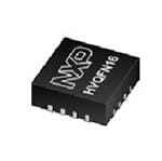
| 产品图片 |
|
| 产品型号 | PCA9672BS,118 |
| PCN封装 | |
| rohs | 无铅 / 符合限制有害物质指令(RoHS)规范要求 |
| 产品系列 | - |
| 中断输出 | 是 |
| 产品培训模块 | http://www.digikey.cn/PTM/IndividualPTM.page?site=cn&lang=zhs&ptm=30172 |
| 供应商器件封装 | 16-HVQFN(3x3) |
| 其它名称 | 568-4194-1 |
| 包装 | 剪切带 (CT) |
| 安装类型 | 表面贴装 |
| 封装/外壳 | 16-VFQFN 裸露焊盘 |
| 工作温度 | -40°C ~ 85°C |
| 接口 | I²C |
| 标准包装 | 1 |
| 特性 | POR |
| 电压-电源 | 2.3 V ~ 5.5 V |
| 电流-灌/拉输出 | 100µA, 25mA |
| 输出类型 | 推挽式 |
| 频率-时钟 | 1MHz |


- 商务部:美国ITC正式对集成电路等产品启动337调查
- 曝三星4nm工艺存在良率问题 高通将骁龙8 Gen1或转产台积电
- 太阳诱电将投资9.5亿元在常州建新厂生产MLCC 预计2023年完工
- 英特尔发布欧洲新工厂建设计划 深化IDM 2.0 战略
- 台积电先进制程称霸业界 有大客户加持明年业绩稳了
- 达到5530亿美元!SIA预计今年全球半导体销售额将创下新高
- 英特尔拟将自动驾驶子公司Mobileye上市 估值或超500亿美元
- 三星加码芯片和SET,合并消费电子和移动部门,撤换高东真等 CEO
- 三星电子宣布重大人事变动 还合并消费电子和移动部门
- 海关总署:前11个月进口集成电路产品价值2.52万亿元 增长14.8%


PDF Datasheet 数据手册内容提取
PCA9672 Remote 8-bit I/O expander for Fm+ I2C-bus with interrupt and reset Rev. 3 — 27 May 2013 Product data sheet 1. General description The PCA9672 provides general-purpose remote I/O expansion via the two-wire bidirectional I2C-bus (serial clock (SCL), serial data (SDA)). The devices consist of eight quasi-bidirectional ports, 1MHz 30mA drive I2C-bus interface, three hardware address inputs and a reset input operating between 2.3V and 5.5V. 1MHz I2C-bus Fast-mode Plus (Fm+) can support PWM dimming of LEDs, and higher I2C-bus drive 30mA allows more devices to be on the bus without the need for bus buffers. The quasi-bidirectional port can be independently assigned as an input to monitor interrupt status or keypads, or as an output to activate indicator devices such as LEDs. The system master can read from the input port or write to the output port through a single register. The low current consumption of 2.5A (typical, static) is great for mobile applications and the latched output ports have 25mA high current sink drive capability for directly driving LEDs. The PCA9672 has two hardware address pins, allowing sixteen of each device to be on the same I2C-bus without the need for bus buffers, so there can be supporting up to 128I/Os (for example, 128LEDs). The active LOW open-drain interrupt output (INT) can be connected to the interrupt logic of the microcontroller and is activated when any input state differs from its corresponding input port register state. It is used to indicate to the microcontroller that an input state has changed and the device needs to be interrogated without the microcontroller continuously polling the input register via the I2C-bus. The internal Power-On Reset (POR) and active LOW hardware reset pin (RESET) initialize the I/Os as inputs with a weak internal pull-up 100A current source. 2. Features and benefits I2C-bus to parallel port expander 1MHz I2C-bus interface (Fast-mode Plus I2C-bus) Operating supply voltage 2.3V to 5.5V with 5.5V tolerant I/Os held to V with DD 100A current source 8-bit remote I/O pins that default to inputs at power-up Latched outputs with 25mA sink capability directly drive LEDs Total package sink capability of 200mA Active LOW reset input Active LOW open-drain interrupt output
PCA9672 NXP Semiconductors Remote 8-bit I/O expander for Fm+ I2C-bus with interrupt and reset Sixteen programmable slave addresses using two address pins Readable device ID (manufacturer, device type, and revision) Software reset Low standby current (2.5A typical) 40C to +85C operation ESD protection exceeds 2000V HBM per JESD22-A114 and 1000V CDM per JESD22-C101 Latch-up testing is done to JEDEC standard JESD78 which exceeds 100 mA Packages offered: SO16, TSSOP16 and HVQFN16 3. Applications LED signs and displays Servers Keypads Industrial control Medical equipment PLCs Cellular telephones Mobile devices Gaming machines Instrumentation and test measurement 4. Ordering information Table 1. Ordering info rmation Type number Topside Package marking Name Description Version PCA9672BS 672 HVQFN1 plastic thermal enhanced very thin quad flatpackage; noleads; SOT758-1 6 16terminals; body330.85mm PCA9672D PCA9672D SO16 plastic small outline package; 16 leads; bodywidth 7.5mm SOT162-1 PCA9672PW PCA9672 TSSOP16 plastic thin shrink small outline package; 16leads; bodywidth4.4mm SOT403-1 4.1 Ordering options Table 2. Ordering opt ions Type number Orderable Package Packing method Minimum Temperature range partnumber order quantity PCA9672BS PCA9672BS,118 HVQFN16 Reel 13” Q1/T1 *standardmarkSMD 6000 T =40C to +85C amb PCA9672D PCA9672D,512 SO16 Standard marking * tube dry pack 1920 T =40C to +85C amb PCA9672D,518 SO16 Reel 13” Q1/T1 *standardmark SMD 1000 T =40C to +85C amb drypack PCA9672PW PCA9672PW,112 TSSOP16 Standard marking * IC’s tube - 2400 T =40C to +85C amb DSCdry pack PCA9672PW,118 TSSOP16 Reel 13” Q1/T1 *standardmarkSMD 2500 T =40C to +85C amb PCA9672 All information provided in this document is subject to legal disclaimers. © NXP B.V. 2013. All rights reserved. Product data sheet Rev. 3 — 27 May 2013 2 of 36
PCA9672 NXP Semiconductors Remote 8-bit I/O expander for Fm+ I2C-bus with interrupt and reset 5. Block diagram PCA9672 INTERRUPT INT LP FILTER LOGIC AD0 AD1 SCL INPUT I2C-BUS SHIFT I/O FILTER CONTROL REGISTER 8 BITS PORT P0 to P7 SDA write pulse RESET POWER-ON read pulse VDD RESET VSS 002aac321 Fig 1. Block diagram of PCA9672 VDD write pulse IOH 100 µA Itrt(pu) data from Shift Register D Q FF P0 to P7 CI IOL S power-on reset VSS D Q FF read pulse CI S to interrupt logic data to Shift Register 002aah521 Fig 2. Simplified schematic diagram of P0 to P7 PCA9672 All information provided in this document is subject to legal disclaimers. © NXP B.V. 2013. All rights reserved. Product data sheet Rev. 3 — 27 May 2013 3 of 36
PCA9672 NXP Semiconductors Remote 8-bit I/O expander for Fm+ I2C-bus with interrupt and reset 6. Pinning information 6.1 Pinning AD0 1 16 VDD AD0 1 16 VDD AD1 2 15 SDA AD1 2 15 SDA RESET 3 14 SCL RESET 3 14 SCL P0 4 13 INT P0 4 13 INT PCA9672D PCA9672PW P1 5 12 P7 P1 5 12 P7 P2 6 11 P6 P2 6 11 P6 P3 7 10 P5 P3 7 10 P5 VSS 8 9 P4 VSS 8 9 P4 002aac322 002aac323 Fig 3. Pin configuration for SO16 Fig 4. Pin configuration for TSSOP16 1 0 D A terminal 1 D D D D A A V S index area 6 5 4 3 1 1 1 1 RESET 1 12 SCL P0 2 11 INT PCA9672BS P1 3 10 P7 P2 4 9 P6 5 6 7 8 3 S 4 5 P S P P V 002aac325 Transparent top view Fig 5. Pin configuration for HVQFN16 6.2 Pin description Table 3. Pin description Symbol Pin Description SO16, TSSOP16 HVQFN16 AD0 1 15 address input 0 AD1 2 16 address input 1 RESET 3 1 reset input (active LOW) P0 4 2 quasi-bidirectional I/O0 P1 5 3 quasi-bidirectional I/O1 P2 6 4 quasi-bidirectional I/O2 P3 7 5 quasi-bidirectional I/O3 V 8 6[1] supply ground SS P4 9 7 quasi-bidirectional I/O4 P5 10 8 quasi-bidirectional I/O5 P6 11 9 quasi-bidirectional I/O6 PCA9672 All information provided in this document is subject to legal disclaimers. © NXP B.V. 2013. All rights reserved. Product data sheet Rev. 3 — 27 May 2013 4 of 36
PCA9672 NXP Semiconductors Remote 8-bit I/O expander for Fm+ I2C-bus with interrupt and reset Table 3. Pin description …continued Symbol Pin Description SO16, TSSOP16 HVQFN16 P7 12 10 quasi-bidirectional I/O7 INT 13 11 interrupt output (activeLOW) SCL 14 12 serial clock line SDA 15 13 serial data line V 16 14 supply voltage DD [1] HVQFN16 package die supply ground is connected to both the V pin and the exposed center pad. The SS VSS pin must be connected to supply ground for proper device operation. For enhanced thermal, electrical, and board-level performance, the exposed pad needs to be soldered to the board using a corresponding thermal pad on the board, and for proper heat conduction through the board thermal vias need to be incorporated in the PCB in the thermal pad region. 7. Functional description Refer to Figure 1 “Block diagram of PCA9672”. 7.1 Device address Following a START condition, the bus master must send the address of the slave it is accessing and the operation it wants to perform (read or write). The address format of the PCA9672 is shown in Figure6. Slave address pins AD1 and AD0 are used to choose one of 16slave addresses. These devices can monitor the change in SDA or SCL in addition to the static levels of V or V to decode four states allowing a larger address range. To DD SS conserve power, no internal pull-up resistors are incorporated on AD1 or AD0, so they must be externally connected to V , V directly or through resistors, or to SCL or SDA DD SS directly. Address values depending on AD1 and AD0 can be found in Table 4 “PCA9672 address map”. Remark: When using the PCA9672 reserved I2C-bus addresses must be used with caution since they can interfere with: • “reserved for future use” I2C-bus addresses (0000011, 1111101, 1111110, 1111111) • slave devices that use the 10-bit addressing scheme (11110xx) • High speed mode (Hs-mode) master code (00001xx) slave address A6 A5 A4 A3 A2 A1 A0 R/W programmable 002aab636 Fig 6. PCA9672 address The last bit of the first byte defines the operation to be performed. When set to logic1 a read is selected, while a logic0 selects a write operation. When AD1 and AD0 are held to V or V , the same address as the PCF8574 or the DD SS newer PCA8574 with A2 held to V is applied. SS PCA9672 All information provided in this document is subject to legal disclaimers. © NXP B.V. 2013. All rights reserved. Product data sheet Rev. 3 — 27 May 2013 5 of 36
PCA9672 NXP Semiconductors Remote 8-bit I/O expander for Fm+ I2C-bus with interrupt and reset 7.1.1 Address map Table 4. PCA9672 address map Pin connectivity Address of PCA9672 Address byte value 7-bit hexadecimal AD1 AD0 A6 A5 A4 A3 A2 A1 A0 R/W Write Read address without R/W SCL V 0 0 1 0 0 0 0 - 20h 21h 10h SS SCL V 0 0 1 0 0 0 1 - 22h 23h 11h DD SDA V 0 0 1 0 0 1 0 - 24h 25h 12h SS SDA V 0 0 1 0 0 1 1 - 26h 27h 13h DD SCL SCL 0 0 1 1 0 0 0 - 30h 31h 18h SCL SDA 0 0 1 1 0 0 1 - 32h 33h 19h SDA SCL 0 0 1 1 0 1 0 - 34h 35h 1Ah SDA SDA 0 0 1 1 0 1 1 - 36h 37h 1Bh V V 0 1 0 0 0 0 0 - 40h 41h 20h SS SS V V 0 1 0 0 0 0 1 - 42h 43h 21h SS DD V V 0 1 0 0 0 1 0 - 44h 45h 22h DD SS V V 0 1 0 0 0 1 1 - 46h 47h 23h DD DD V SCL 0 1 0 1 0 0 0 - 50h 51h 28h SS V SDA 0 1 0 1 0 0 1 - 52h 53h 29h SS V SCL 0 1 0 1 0 1 0 - 54h 55h 2Ah DD V SDA 0 1 0 1 0 1 1 - 56h 57h 2Bh DD 7.2 Software Reset Call, and device ID addresses Two other different addresses can be sent to the PCA9672. • General Call address: allows to reset the PCA9672 through the I2C-bus upon reception of the right I2C-bus sequence. See Section 7.2.1 “Software Reset” for more information. • Device ID address: allows to read ID information from the device (manufacturer, part identification, revision). See Section 7.2.2 “Device ID (PCA9672 ID field)” for more information. R/W 0 0 0 0 0 0 0 0 002aac115 Fig 7. General Call address 1 1 1 1 1 0 0 R/W 002aac116 Fig 8. Device ID address PCA9672 All information provided in this document is subject to legal disclaimers. © NXP B.V. 2013. All rights reserved. Product data sheet Rev. 3 — 27 May 2013 6 of 36
PCA9672 NXP Semiconductors Remote 8-bit I/O expander for Fm+ I2C-bus with interrupt and reset 7.2.1 Software Reset The Software Reset Call allows all the devices in the I2C-bus to be reset to the power-up state value through a specific formatted I2C-bus command. To be performed correctly, it implies that the I2C-bus is functional and that there is no device hanging the bus. The Software Reset sequence is defined as following: 1. A START command is sent by the I2C-bus master. 2. The reserved General Call I2C-bus address ‘0000000’ with the R/W bit set to 0 (write) is sent by the I2C-bus master. 3. The PCA9672 device(s) acknowledge(s) after seeing the General Call address ‘00000000’ (00h) only. If the R/W bit is set to 1 (read), no acknowledge is returned to the I2C-bus master. 4. Once the General Call address has been sent and acknowledged, the master sends 1byte. The value of the byte must be equal to 06h. a. The PCA9672 acknowledges this value only. If the byte is not equal to 06h, the PCA9672 does not acknowledge it. If more than 1byte of data is sent, the PCA9672 does not acknowledge any more. 5. Once the right byte has been sent and correctly acknowledged, the master sends a STOP command to end the Software Reset sequence: the PCA9672 then resets to the default value (power-up value) and is ready to be addressed again within the specified bus free time. If the master sends a Repeated START instead, no reset is performed. The I2C-bus master must interpret a non-acknowledge from the PCA9672 (at any time) as a ‘Software Reset Abort’. The PCA9672 does not initiate a reset of its registers. The unique sequence that initiates a Software Reset is described in Figure9. SWRST Call I2C-bus address SWRST data = 06h S 0 0 0 0 0 0 0 0 A 0 0 0 0 0 1 1 0 A P START condition R/W acknowledge from slave(s) acknowledge from slave(s) PCA9672 is(are) reset. Registers are set to default power-up values. 002aac329 Fig 9. Software Reset sequence Simple code for Software Reset: <S> <00h> <ACK> <06h> <ACK> <P> PCA9672 All information provided in this document is subject to legal disclaimers. © NXP B.V. 2013. All rights reserved. Product data sheet Rev. 3 — 27 May 2013 7 of 36
PCA9672 NXP Semiconductors Remote 8-bit I/O expander for Fm+ I2C-bus with interrupt and reset 7.2.2 Device ID (PCA9672 ID field) The Device ID field is a 3-byte read-only (24bits) word giving the following information: • 12bits with the manufacturer name, unique per manufacturer (for example, NXP). • 9bits with the part identification, assigned by manufacturer. • 3bits with the die revision, assigned by manufacturer (for example, Rev X). The Device ID is read-only, hardwired in the device and can be accessed as follows: 1. START command 2. The master sends the Reserved Device ID I2C-bus address ‘1111100’ with the R/W bit set to 0 (write). 3. The master sends the I2C-bus slave address of the slave device it needs to identify. The LSB is a ‘Don’t care’ value. Only one device must acknowledge this byte (the one that has the I2C-bus slave address). 4. The master sends a Re-START command. Remark: A STOP command followed by a START command will reset the slave state machine and the Device ID read cannot be performed. Remark: A STOP command or a Re-START command followed by an access to another slave device will reset the slave state machine and the Device ID read cannot be performed. 5. The master sends the Reserved Device ID I2C-bus address ‘1111100’ with the R/W bit set to 1 (read). 6. The device ID read can be done, starting with the 12 manufacturer bits (first byte+ 4MSB of the second byte), followed by the 9 part identification bits and then the 3dierevision bits (3LSB of the third byte). 7. The master ends the reading sequence by NACKing the last byte, thus resetting the slave device state machine and allowing the master to send the STOP command. Remark: The reading of the Device ID can be stopped anytime by sending a NACK command. Remark: If the master continues to ACK the bytes after the third byte, the PCA9672 rolls back to the first byte and keeps sending the Device ID sequence until a NACK has been detected. For the PCA9672, the Device ID is as shown in Figure10. manufacturer 0 0 0 0 0 0 0 0 0 0 0 0 part identification 0 0 1 0 0 0 0 1 1 revision 0 0 0 002aac326 Fig 10. PCA9672 Device ID field PCA9672 All information provided in this document is subject to legal disclaimers. © NXP B.V. 2013. All rights reserved. Product data sheet Rev. 3 — 27 May 2013 8 of 36
PCA9672 NXP Semiconductors Remote 8-bit I/O expander for Fm+ I2C-bus with interrupt and reset acknowledge from acknowledge from acknowledge from one or several slaves I2C-bus slave address slave to be identified slave to be identified Device ID address of the device to be identified Device ID address S 1 1 1 1 1 0 0 0 A A6 A5 A4 A3 A2 A1 A0 0 A Sr 1 1 1 1 1 0 0 1 A START condition R/W don’t care repeated START R/W condition acknowledge acknowledge no acknowledge from master from master from master M M M9M8M7M6M5M4 A M3M2M1M0P8 P7 P6 P5 A P4 P3 P2 P1 P0 R2 R1 R0 A P 11 10 STOP condition manufacturer name = 000000000000 part identification = 001000011 revision = 000 002aac327 If more than 2 bytes are read, the slave device loops back to the first byte (manufacturer byte) and keeps sending data until the master generates a ‘no acknowledge’. Fig 11. Device ID field reading PCA9672 Simple code for reading Device ID: <S> <F8h> <ACK> <slave address> <ACK> <Sr> <F9h > <ACK> <DATA1> <ACK><DATA2> <ACK> <DATA3> <NACK> <P> 8. I/O programming 8.1 Quasi-bidirectional I/Os A quasi-bidirectional I/O is an input or output port without using a direction control register. Whenever the master reads the register, the value returned to master depends on the actual voltage or status of the pin. At power-on, all the ports are HIGH with a weak 100A internal pull-up to V , but can be driven LOW by an internal transistor, or an external DD signal. The I/O ports are entirely independent of each other, but each I/O octal is controlled by the same read or write data byte. Advantages of the quasi-bidirectional I/O over totem pole I/O include: • Better for driving LEDs since the p-channel (transistor to V ) is small, which saves DD die size and therefore cost. LED drive only requires an internal transistor to ground, while the LED is connected to V through a current-limiting resistor. Totempole I/O DD have both n-channel and p-channel transistors, which allow solid HIGH and LOW output levels without a pull-up resistor — good for logic levels. • Simpler architecture — only a single register and the I/O can be both input and output at the same time. Totem pole I/O have a direction register that specifies the port pin direction and it is always in that configuration unless the direction is explicitly changed. • Doesnot require a command byte. The simplicity of one register (no need for the pointer register or, technically, the command byte) is an advantage in some embedded systems where every byte counts because of memory or bandwidth limitations. PCA9672 All information provided in this document is subject to legal disclaimers. © NXP B.V. 2013. All rights reserved. Product data sheet Rev. 3 — 27 May 2013 9 of 36
PCA9672 NXP Semiconductors Remote 8-bit I/O expander for Fm+ I2C-bus with interrupt and reset There is only one register to control four possibilities of the port pin: Input HIGH, input LOW, output HIGH, or output LOW. Input HIGH: The master needs to write 1 to the register to set the port as an input mode if the device is not in the default power-on condition. The master reads the register to check the input status. If the external source pulls the port pin up to V or drives DD logic1, then the master will read the value of 1. Input LOW: The master needs to write 1 to the register to set the port to input mode if the device is not in the default power-on condition. The master reads the register to check the input status. If the external source pulls the port pin down to V or drives SS logic0, which sinks the weak 100A current source, then the master will read the value of 0. Output HIGH: The master writes 1 to the register. There is an additional ‘accelerator’ or strong pull-up current when the master sets the port HIGH. The additional strong pull-up is only active during the HIGH time of the acknowledge clock cycle. This accelerator current helps the port’s 100A current source make a faster rising edge into a heavily loaded output, but only at the start of the acknowledge clock cycle to avoid bus contention if an external signal is pulling the port LOW to V /driving the port with SS logic0 at the same time. After the half clock cycle there is only the 100A current source to hold the port HIGH. Output LOW: The master writes 0 to the register. There is a strong current sink transistor that holds the port pin LOW. A large current may flow into the port, which could potentially damage the part if the master writes a 0 to the register and an external source is pulling the port HIGH at the same time. VDD input HIGH weak 100 µA pull-up with current source output HIGH (inactive when resistor to VDD or output LOW) external drive HIGH accelerator pull-up P port P7 - P0 pull-down with output LOW resistor to VSS or external drive LOW input LOW VSS 002aah683 Fig 12. Simple quasi-bidirectional I/O PCA9672 All information provided in this document is subject to legal disclaimers. © NXP B.V. 2013. All rights reserved. Product data sheet Rev. 3 — 27 May 2013 10 of 36
PCA9672 NXP Semiconductors Remote 8-bit I/O expander for Fm+ I2C-bus with interrupt and reset 8.2 Writing to the port (Output mode) The master (microcontroller) sends the START condition and slave address setting the last bit of the address byte to logic0 for the write mode. The PCA9672 acknowledges and the master then sends the data byte for P7 to P0 to the port register. As the clock line goes HIGH, the 8-bit data is presented on the port lines after it has been acknowledged by the PCA9672. If a LOW is written, the strong pull-down turns on and stays on. If a HIGH is written, the strong pull-up turns on for 1⁄ of the clock cycle, then the line is held HIGH by 2 the weak current source. The master can then send a STOP or ReSTART condition or continue sending data. The number of data bytes that can be sent successively is not limited and the previous data is overwritten every time a data byte has been sent and acknowledged. Ensure a logic1 is written for any port that is being used as an input to ensure the strong external pull-down is turned off. SCL 1 2 3 4 5 6 7 8 9 slave address data 1 data 2 SDA S A6 A5 A4 A3 A2 A1 A0 0 A P7 P6 1 P4 P3 P2 P1 P0 A P7 P6 0 P4 P3 P2 P1 P0 A START condition R/W P5 P5 acknowledge acknowledge acknowledge from slave from slave from slave write to port tv(Q) tv(Q) data output from port DATA 1 VALID DATA 2 VALID P5 output voltage P5 pull-up output current Itrt(pu) IOH INT trst(INT) 002aah623 Fig 13. Write mode (output) Simple code for Write cycle: <S> <slave address + W> <ACK> <DATA1> <ACK> <DATA2> <ACK> <DATA1> ... <DATAn><ACK><P> PCA9672 All information provided in this document is subject to legal disclaimers. © NXP B.V. 2013. All rights reserved. Product data sheet Rev. 3 — 27 May 2013 11 of 36
PCA9672 NXP Semiconductors Remote 8-bit I/O expander for Fm+ I2C-bus with interrupt and reset 8.3 Reading from a port (Input mode) The port must have been previously written to logic1, which is the condition after power-on reset or hardware reset or software reset. To enter the Read mode, the master (microcontroller) addresses the slave device and sets the last bit of the address byte to logic1 (address byte read). The slave will acknowledge and then send the data byte to the master. The master will NACK and then send the STOP condition or ACK and read the input register again. The read of any pin being used as an output will indicate HIGH or LOW depending on the actual state of the input pin. If the data on the input port changes faster than the master can read, this data may be lost. The DATA2 and DATA3 are lost because these data did not meet the set-up time and hold time (see Figure14). no acknowledge from master slave address data from port data from port SDA S A6 A5 A4 A3 A2 A1 A0 1 A DATA 1 A DATA 4 1 P START condition R/W acknowledge acknowledge STOP from slave from master condition read from port DATA 2 data at DATA 1 DATA 3 DATA 4 port th(D) tsu(D) INT tv(INT) trst(INT) trst(INT) 002aah383 A LOW-to-HIGH transition of SDA while SCL is HIGH is defined as the STOP condition (P). Transfer of data can be stopped at any moment by a STOP condition. When this occurs, data present at the last acknowledge phase is valid (Output mode). Input data is lost. Fig 14. Read input port register Simple code for Read cycle: <S> <slave address + R> <ACK> <DATA in> <ACK> <DATA in> ... <NACK> <P> 8.4 Power-on reset When power is applied to V , an internal Power-On Reset (POR) holds the PCA9672 in DD a reset condition until V has reached V . At that point, the reset condition is released DD POR and the PCA9672 registers and I2C-bus/SMBus state machine will initialize to their default states of all I/Os to inputs with weak current source to V . Thereafter V must be DD DD lowered below V and back up to the operation voltage for power-on reset cycle. POR PCA9672 All information provided in this document is subject to legal disclaimers. © NXP B.V. 2013. All rights reserved. Product data sheet Rev. 3 — 27 May 2013 12 of 36
PCA9672 NXP Semiconductors Remote 8-bit I/O expander for Fm+ I2C-bus with interrupt and reset 8.5 Interrupt output (INT) The PCA9672 provides an open-drain output (INT) which can be fed to a corresponding input of the microcontroller (see Figure15). As soon as a port input is changed, the INT will be active (LOW) and notify the microcontroller. An interrupt is generated at any rising or falling edge of the port inputs. After time t , the v(Q) signal INT is valid. The interrupt will reset to HIGH when data on the port is changed to the original setting or data is read or written by the master. In the Write mode, the interrupt may be reset (HIGH) on the rising edge of the acknowledge bit of the data byte and also on the rising edge of the write to port pulse. The interrupt will always be reset (HIGH) on the falling edge of the write to port pulse (see Figure13). The interrupt is reset (HIGH) in the rising edge of the read from port pulse (see Figure14). During the interrupt reset, any I/O change close to the read or write pulse may not generate an interrupt, or the interrupt will have a very short pulse. After the interrupt is reset, any change in I/Os will be detected and transmitted as an INT. At power-on reset all ports are in Input mode and the initial state of the ports is HIGH, therefore, for any port pin that is pulled LOW or driven LOW by external source, the interrupt output will be active (output LOW). VDD device 1 device 2 device 8 PCA9672 PCA9672 PCA9672 MICROCOMPUTER INT INT INT INT 002aac328 Fig 15. Application of multiple PCA9672s with interrupt 8.6 RESET input A reset can be accomplished by holding the RESET pin LOW for a minimum of t . The w(rst) PCA9672 registers and I2C-bus state machine will be held in their default state until the RESET input is once again HIGH. The RESET input pin requires a pull-up resistor to V DD if no active connection is used. PCA9672 All information provided in this document is subject to legal disclaimers. © NXP B.V. 2013. All rights reserved. Product data sheet Rev. 3 — 27 May 2013 13 of 36
PCA9672 NXP Semiconductors Remote 8-bit I/O expander for Fm+ I2C-bus with interrupt and reset 9. Characteristics of the I2C-bus The I2C-bus is for 2-way, 2-line communication between different ICs or modules. The two lines are a serial data line (SDA) and a serial clock line (SCL). Both lines must be connected to a positive supply via a pull-up resistor when connected to the output stages of a device. Data transfer may be initiated only when the bus is not busy. 9.1 Bit transfer One data bit is transferred during each clock pulse. The data on the SDA line must remain stable during the HIGH period of the clock pulse as changes in the data line at this time will be interpreted as control signals (see Figure16). SDA SCL data line change stable; of data data valid allowed mba607 Fig 16. Bit transfer 9.1.1 START and STOP conditions Both data and clock lines remain HIGH when the bus is not busy. A HIGH-to-LOW transition of the data line while the clock is HIGH is defined as the START condition (S). ALOW-to-HIGH transition of the data line while the clock is HIGH is defined as the STOP condition (P) (see Figure17.) SDA SCL S P START condition STOP condition mba608 Fig 17. Definition of START and STOP conditions 9.2 System configuration A device generating a message is a ‘transmitter'; a device receiving is the ‘receiver'. The device that controls the message is the ‘master' and the devices which are controlled by the master are the ‘slaves' (see Figure18). PCA9672 All information provided in this document is subject to legal disclaimers. © NXP B.V. 2013. All rights reserved. Product data sheet Rev. 3 — 27 May 2013 14 of 36
PCA9672 NXP Semiconductors Remote 8-bit I/O expander for Fm+ I2C-bus with interrupt and reset SDA SCL MASTER SLAVE SLAVE MASTER MASTER I2C-BUS TRANSMITTER/ RECEIVER TRANSMITTER/ TRANSMITTER TRANSMITTER/ MULTIPLEXER RECEIVER RECEIVER RECEIVER SLAVE 002aaa966 Fig 18. System configuration 9.3 Acknowledge The number of data bytes transferred between the START and the STOP conditions from transmitter to receiver is not limited. Each byte of eightbits is followed by one acknowledge bit. The acknowledge bit is an active LOW level (generated by the receiving device) that indicates to the transmitter that the data transfer was successful. A slave receiver which is addressed must generate an acknowledge after the reception of each byte. Also a master must generate an acknowledge after the reception of each byte that has been clocked out of the slave transmitter. The device that wants to issue an acknowledge bit has to pull down the SDA line during the acknowledge clock pulse, so that the SDA line is stable LOW during the HIGH period of the acknowledge bit related clock pulse; set-up and hold times must be taken into account. A master receiver must signal an end of data to the transmitter by not generating an acknowledge on the last byte that has been clocked out of the slave. In this event, the transmitter must leave the data line HIGH to enable the master to generate a STOP condition. data output by transmitter not acknowledge data output by receiver acknowledge SCL from master 1 2 8 9 S clock pulse for START acknowledgement condition 002aaa987 Fig 19. Acknowledgement on the I2C-bus PCA9672 All information provided in this document is subject to legal disclaimers. © NXP B.V. 2013. All rights reserved. Product data sheet Rev. 3 — 27 May 2013 15 of 36
PCA9672 NXP Semiconductors Remote 8-bit I/O expander for Fm+ I2C-bus with interrupt and reset 10. Application design-in information 10.1 Bidirectional I/O expander applications In the 8-bit I/O expander application shown in Figure20, P0 and P1 are inputs, and P2 to P7 are outputs. When used in this configuration, during a write, the input (P0 and P1) must be written as HIGH so the external devices fully control the input ports. The desired HIGH or LOW logic levels may be written to the I/Os used as outputs (P2 to P7). If10A internal output HIGH is not enough current source, the port needs external pull-up resistor. During a read, the logic levels of the external devices driving the input ports (P0 and P1) and the previous written logic level to the output ports (P2 to P7) will be read. The GPIO also has an interrupt line (INT) that can be connected to the interrupt logic of the microprocessor. By sending an interrupt signal on this line, the remote I/O informs the microprocessor that there has been a change of data on its ports without having to communicate via the I2C-bus. The GPIO also has a reset line (RESET) that can be connected to an output pin of the microcontroller. VDD VDD VDD SDA P0 temperature sensor CORE SCL P1 battery status PROCESSOR INT P2 control for latch RESET P3 control for switch P4 control for audio P5 control for camera AD0 P6 control for MP3 AD1 P7 002aac330 Fig 20. Bidirectional I/O expander application 10.2 How to read and write to I/O expander (example) In the application example of PCA9672 shown in Figure20, the microcontroller wants to control the P3 switch ON and the P7 LED ON when the temperature sensor P0 changes. 1. When the system power on: Core Processor needs to issue an initial command to set P0 and P1 as inputs and P[7:2] as outputs with value 101000 (LED off, MP3 off, camera on, audio off, switchoff and latch off). 2. Operation: When the temperature changes above the threshold, the temperature sensor signal will toggle from HIGH to LOW. The INT will be activated and notifies the ‘core processor’, that there have been changes on the input pins. Read the input register. IfP0=0 (temperature sensor has changed), then turn on LED and turn on switch. PCA9672 All information provided in this document is subject to legal disclaimers. © NXP B.V. 2013. All rights reserved. Product data sheet Rev. 3 — 27 May 2013 16 of 36
PCA9672 NXP Semiconductors Remote 8-bit I/O expander for Fm+ I2C-bus with interrupt and reset 3. Software code: //System Power on // write to PCA9672 with data 1010 0011b to set P[7:2] outputs and P[1:0] inputs <S> <0100 0000> <ACK> <1010 0011> <ACK> <P>//Initial setting for PCA9672 while (INT == 1); //Monitor the interrupt pin. If INT = 1 do nothing //When INT = 0 then read input ports <S> <slave address read> <ACK> <1010 0010> <NACK> <P> //Read PCA9672 data If (P0 == 0) //Temperature sensor activated { // write to PCA9672 with data 0010 1011b to turn on LED (P7), on Switch (P3) and keep P[1:0] as input ports. <S> <0100 0000> <ACK> <0010 1011> <ACK> <P> // Write to PCA9672 } 10.3 High current-drive load applications The GPIO has a minimum guaranteed sinking current of 25mA per bit at 5V. In applications requiring additional drive, two port pins may be connected together to sink up to 50mA current. Both bits must then always be turned on or off together. Up to 8pins can be connected together to drive 200mA, which is the device recommended total limit. Each pin needs its own limiting resistor as shown in Figure21 to prevent damage to the device should all ports not be turned on at the same time. VDD VDD VDD SDA P0 CORE SCL P1 PROCESSOR INT P2 RESET P3 LOAD P4 P5 AD0 P6 AD1 P7 002aac331 Fig 21. High current-drive load application 10.4 Migration path NXP offers newer, more capable drop-in replacements for the PCF8574/74A in newer space-saving packages. Table 5. Migration pa th Type number I2C-bus Voltage range Number of Interrupt Reset Total package frequency addresses sink current perdevice PCF8574/74A 100kHz 2.5V to 6V 8 yes no 80mA PCA8574/74A 400kHz 2.3V to 5.5V 8 yes no 200mA PCA9674/74A 1MHz Fm+ 2.3V to 5.5V 64 yes no 200mA PCA9670 1MHz Fm+ 2.3V to 5.5V 64 no yes 200mA PCA9672 1MHz Fm+ 2.3V to 5.5V 16 yes yes 200mA PCA9672 All information provided in this document is subject to legal disclaimers. © NXP B.V. 2013. All rights reserved. Product data sheet Rev. 3 — 27 May 2013 17 of 36
PCA9672 NXP Semiconductors Remote 8-bit I/O expander for Fm+ I2C-bus with interrupt and reset PCA9670 replaces the interrupt output of the PCA9674 with hardware reset input to retain the maximum number of addresses. The PCA9672 replaces address A2 of the PCA9674 with hardware reset input to retain the interrupt, but limit the number of addresses. 11. Limiting values Table 6. Limiting values In accordance with the Absolute Maximum Rating System (IEC 60134). Symbol Parameter Conditions Min Max Unit V supply voltage 0.5 +6 V DD I supply current - 100 mA DD I ground supply current - 400 mA SS V input voltage V 0.5 5.5 V I SS I input current - 20 mA I I output current [1] - 50 mA O P total power dissipation - 400 mW tot P/out power dissipation per output - 100 mW T maximum junction temperature - 125 C j(max) T storage temperature 65 +150 C stg T ambient temperature operating 40 +85 C amb [1] Total package (maximum) output current is 400mA. 12. Thermal characteristics Table 7. Thermal characteristics Symbol Parameter Conditions Typ Unit R thermal resistance from junction SO16 package 115 C/W th(j-a) to ambient TSSOP16 package 160 C/W HVQFN16 package 40 C/W PCA9672 All information provided in this document is subject to legal disclaimers. © NXP B.V. 2013. All rights reserved. Product data sheet Rev. 3 — 27 May 2013 18 of 36
PCA9672 NXP Semiconductors Remote 8-bit I/O expander for Fm+ I2C-bus with interrupt and reset 13. Static characteristics Table 8. Static charac teristics V =2.3V to 5.5V; V =0V; T =40Cto+85C; unless otherwise specified. DD SS amb Symbol Parameter Conditions Min Typ Max Unit Supplies V supply voltage 2.3 - 5.5 V DD I supply current Operating mode; no load; - 260 500 A DD V =V or V ; f =1MHz; I DD SS SCL AD0, AD1=static H or L I standby current Standby mode; no load; - 2.5 10 A stb V =V or V ; f =0kHz I DD SS SCL V power-on reset voltage [1] - 1.8 2.0 V POR Input SCL; input/output SDA V LOW-level input voltage 0.5 - +0.3V V IL DD V HIGH-level input voltage 0.7V - 5.5 V IH DD I LOW-level output current V =0.4V; V =2.3V 20 - - mA OL OL DD V =0.4V; V =3.0V 25 - - mA OL DD V =0.4V; V =4.5V 30 - - mA OL DD I leakage current V =V orV 1 - +1 A L I DD SS C input capacitance V =V - 4 10 pF i I SS I/Os; P0 to P7 V LOW-level input voltage 0.5 - +0.3V V IL DD V HIGH-level input voltage 0.7V - 5.5 V IH DD I LOW-level output current V =0.5V; V =2.3V [2] 12 28 - mA OL OL DD V =0.5V; V =3.0V [2] 17 35 - mA OL DD V =0.5V; V =4.5V [2] 25 43 - mA OL DD I total LOW-level output current V =0.5V; V =4.5V [2] - - 200 mA OL(tot) OL DD I HIGH-level output current V =V 30 250 300 A OH OH SS I transient boosted pull-up current V =V ; see Figure13 0.5 1.0 - mA trt(pu) OH SS C input capacitance [3] - 3 10 pF i C output capacitance [3] - 3 10 pF o Input RESET V LOW-level input voltage 0.5 - +0.8 V IL V HIGH-level input voltage 2 - 5.5 V IH I input leakage current 1 - +1 A LI C input capacitance - 3 5 pF i Interrupt INT (see Figure13 and Figure14) I LOW-level output current V =0.4V 3.0 - - mA OL OL C output capacitance - 2 5 pF o PCA9672 All information provided in this document is subject to legal disclaimers. © NXP B.V. 2013. All rights reserved. Product data sheet Rev. 3 — 27 May 2013 19 of 36
PCA9672 NXP Semiconductors Remote 8-bit I/O expander for Fm+ I2C-bus with interrupt and reset Table 8. Static characteristics …continued V =2.3V to 5.5V; V =0V; T =40Cto+85C; unless otherwise specified. DD SS amb Symbol Parameter Conditions Min Typ Max Unit Inputs AD0, AD1 V LOW-level input voltage 0.5 - +0.3V V IL DD V HIGH-level input voltage 0.7V - 5.5 V IH DD I input leakage current 1 - +1 A LI C input capacitance - 3 5 pF i [1] The power-on reset circuit resets the I2C-bus logic with V <V and set all I/Os to logic1 (with current source to V ). DD POR DD [2] Each bit must be limited to a maximum of 25mA and the total package limited to 200mA due to internal busing limits. [3] The value is not tested, but verified on sampling basis. 14. Dynamic characteristics Table 9. Dynamic cha racteristics V =2.3V to 5.5V; V =0V; T =40Cto+85C; unless otherwise specified. DD SS amb Symbol Parameter Conditions Standardmode Fastmode I2C-bus Fastmode Plus Unit I2C-bus I2C-bus Min Max Min Max Min Max f SCL clock frequency 0 100 0 400 0 1000 kHz SCL t bus free time between a 4.7 - 1.3 - 0.5 - s BUF STOP and START condition t hold time (repeated) 4.0 - 0.6 - 0.26 - s HD;STA START condition t set-up time for a repeated 4.7 - 0.6 - 0.26 - s SU;STA START condition t set-up time for STOP 4.0 - 0.6 - 0.26 - s SU;STO condition t data hold time 0 - 0 - 0 - ns HD;DAT t data valid acknowledge [1] 0.3 3.45 0.1 0.9 0.05 0.45 s VD;ACK time t data valid time [2] 300 - 50 - 50 450 ns VD;DAT t data set-up time 250 - 100 - 50 - ns SU;DAT t LOW period of the SCL 4.7 - 1.3 - 0.5 - s LOW clock t HIGH period of the SCL 4.0 - 0.6 - 0.26 - s HIGH clock t fall time of both SDA and [4][5] - 300 20+0.1C [3] 300 - 120 ns f b SCL signals t rise time of both SDA and - 1000 20+0.1C [3] 300 - 120 ns r b SCL signals t pulse width of spikes that [6] - 50 - 50 - 50 ns SP must be suppressed by the input filter PCA9672 All information provided in this document is subject to legal disclaimers. © NXP B.V. 2013. All rights reserved. Product data sheet Rev. 3 — 27 May 2013 20 of 36
PCA9672 NXP Semiconductors Remote 8-bit I/O expander for Fm+ I2C-bus with interrupt and reset Table 9. Dynamic characteristics …continued V =2.3V to 5.5V; V =0V; T =40Cto+85C; unless otherwise specified. DD SS amb Symbol Parameter Conditions Standardmode Fastmode I2C-bus Fastmode Plus Unit I2C-bus I2C-bus Min Max Min Max Min Max Port timing; C 100pF (see Figure13 and Figure14) L t data output valid time - 4 - 4 - 4 s v(Q) t data input set-up time 0 - 0 - 0 - s su(D) t data input hold time 4 - 4 - 4 - s h(D) Interrupt timing; C 100pF (see Figure13 and Figure14) L t valid time on pin INT from port - 4 - 4 - 4 s v(INT) toINT t reset time on pin INT from SCL - 4 - 4 - 4 s rst(INT) toINT Reset timing (see Figure23) t reset pulse width 4 - 4 - 4 - s w(rst) t reset recovery time 0 - 0 - 0 - s rec(rst) t reset time 100 - 100 - 100 - s rst [1] t =time for Acknowledgement signal from SCL LOW to SDA (out) LOW. VD;ACK [2] t =minimum time for SDA data out to be valid following SCL LOW. VD;DAT [3] C =total capacitance of one bus line in pF. b [4] A master device must internally provide a hold time of at least 300ns for the SDA signal (refer to the V of the SCL signal) in order to IL bridge the undefined region SCL’s falling edge. [5] The maximum t for the SDA and SCL bus lines is specified at 300ns. The maximum fall time for the SDA output stage t is specified at f f 250ns. This allows series protection resistors to be connected between the SDA and the SCL pins and the SDA/SCL bus lines without exceeding the maximum specified t. f [6] Input filters on the SDA and SCL inputs suppress noise spikes less than 50ns. START bit 7 STOP bit 6 bit 0 acknowledge protocol condition MSB condition (A6) (R/W) (A) (S) (A7) (P) tSU;STA tLOW tHIGH 1 / fSCL SCL 0.7 × VDD 0.3 × VDD tBUF tf tr SDA 0.7 × VDD 0.3 × VDD tHD;STA tSU;DAT tHD;DAT tVD;DAT tVD;ACK tSU;STO 002aab175 Rise and fall times refer to V and V . IL IH Fig 22. I2C-bus timing diagram PCA9672 All information provided in this document is subject to legal disclaimers. © NXP B.V. 2013. All rights reserved. Product data sheet Rev. 3 — 27 May 2013 21 of 36
PCA9672 NXP Semiconductors Remote 8-bit I/O expander for Fm+ I2C-bus with interrupt and reset START ACK or read cycle SCL SDA 30 % trst RESET 50 % 50 % 50 % trec(rst) tw(rst) trst 50 % Pn output off 002aac332 Fig 23. Reset timing PCA9672 All information provided in this document is subject to legal disclaimers. © NXP B.V. 2013. All rights reserved. Product data sheet Rev. 3 — 27 May 2013 22 of 36
PCA9672 NXP Semiconductors Remote 8-bit I/O expander for Fm+ I2C-bus with interrupt and reset 15. Package outline HVQFN16: plastic thermal enhanced very thin quad flat package; no leads; 16 terminals; body 3 x 3 x 0.85 mm SOT758-1 D B A terminal 1 index area E A A1 c detail X e1 C 1/2 e v M C A B y1 C y e b w M C 5 8 L 4 9 e Eh e2 1/2 e 1 12 terminal 1 16 13 index area Dh X 0 2.5 5 mm scale DIMENSIONS (mm are the original dimensions) UNIT mAa(1x). A1 b c D(1) Dh E(1) Eh e e1 e2 L v w y y1 0.05 0.30 3.1 1.75 3.1 1.75 0.5 mm 1 0.2 0.5 1.5 1.5 0.1 0.05 0.05 0.1 0.00 0.18 2.9 1.45 2.9 1.45 0.3 Note 1. Plastic or metal protrusions of 0.075 mm maximum per side are not included. OUTLINE REFERENCES EUROPEAN ISSUE DATE VERSION IEC JEDEC JEITA PROJECTION 02-03-25 SOT758-1 - - - MO-220 - - - 02-10-21 Fig 24. Package outline SOT758-1 (HVQFN16) PCA9672 All information provided in this document is subject to legal disclaimers. © NXP B.V. 2013. All rights reserved. Product data sheet Rev. 3 — 27 May 2013 23 of 36
PCA9672 NXP Semiconductors Remote 8-bit I/O expander for Fm+ I2C-bus with interrupt and reset SO16: plastic small outline package; 16 leads; body width 7.5 mm SOT162-1 D E A X c y HE v M A Z 16 9 Q A2 A A1 (A 3 ) pin 1 index θ Lp L 1 8 detail X e w M bp 0 5 10 mm scale DIMENSIONS (inch dimensions are derived from the original mm dimensions) UNIT mAax. A1 A2 A3 bp c D(1) E(1) e HE L Lp Q v w y Z(1) θ 0.3 2.45 0.49 0.32 10.5 7.6 10.65 1.1 1.1 0.9 mm 2.65 0.25 1.27 1.4 0.25 0.25 0.1 0.1 2.25 0.36 0.23 10.1 7.4 10.00 0.4 1.0 0.4 8o 0.012 0.096 0.019 0.013 0.41 0.30 0.419 0.043 0.043 0.035 0o inches 0.1 0.01 0.05 0.055 0.01 0.01 0.004 0.004 0.089 0.014 0.009 0.40 0.29 0.394 0.016 0.039 0.016 Note 1. Plastic or metal protrusions of 0.15 mm (0.006 inch) maximum per side are not included. OUTLINE REFERENCES EUROPEAN ISSUE DATE VERSION IEC JEDEC JEITA PROJECTION 99-12-27 SOT162-1 075E03 MS-013 03-02-19 Fig 25. Package outline SOT162-1 (SO16) PCA9672 All information provided in this document is subject to legal disclaimers. © NXP B.V. 2013. All rights reserved. Product data sheet Rev. 3 — 27 May 2013 24 of 36
PCA9672 NXP Semiconductors Remote 8-bit I/O expander for Fm+ I2C-bus with interrupt and reset TSSOP16: plastic thin shrink small outline package; 16 leads; body width 4.4 mm SOT403-1 D E A X c y HE v M A Z 16 9 Q A2 (A 3 ) A pin 1 index A1 θ Lp L 1 8 detail X w M e bp 0 2.5 5 mm scale DIMENSIONS (mm are the original dimensions) UNIT mAax. A1 A2 A3 bp c D(1) E(2) e HE L Lp Q v w y Z(1) θ mm 1.1 00..1055 00..9850 0.25 00..3109 00..21 54..19 44..53 0.65 66..62 1 00..7550 00..43 0.2 0.13 0.1 00..4006 80oo Notes 1. Plastic or metal protrusions of 0.15 mm maximum per side are not included. 2. Plastic interlead protrusions of 0.25 mm maximum per side are not included. OUTLINE REFERENCES EUROPEAN ISSUE DATE VERSION IEC JEDEC JEITA PROJECTION 99-12-27 SOT403-1 MO-153 03-02-18 Fig 26. Package outline SOT403-1 (TSSOP16) PCA9672 All information provided in this document is subject to legal disclaimers. © NXP B.V. 2013. All rights reserved. Product data sheet Rev. 3 — 27 May 2013 25 of 36
PCA9672 NXP Semiconductors Remote 8-bit I/O expander for Fm+ I2C-bus with interrupt and reset 16. Handling information All input and output pins are protected against ElectroStatic Discharge (ESD) under normal handling. When handling ensure that the appropriate precautions are taken as described in JESD625-A or equivalent standards. 17. Soldering of SMD packages This text provides a very brief insight into a complex technology. A more in-depth account of soldering ICs can be found in Application Note AN10365 “Surface mount reflow soldering description”. 17.1 Introduction to soldering Soldering is one of the most common methods through which packages are attached to Printed Circuit Boards (PCBs), to form electrical circuits. The soldered joint provides both the mechanical and the electrical connection. There is no single soldering method that is ideal for all IC packages. Wave soldering is often preferred when through-hole and Surface Mount Devices (SMDs) are mixed on one printed wiring board; however, it is not suitable for fine pitch SMDs. Reflow soldering is ideal for the small pitches and high densities that come with increased miniaturization. 17.2 Wave and reflow soldering Wave soldering is a joining technology in which the joints are made by solder coming from a standing wave of liquid solder. The wave soldering process is suitable for the following: • Through-hole components • Leaded or leadless SMDs, which are glued to the surface of the printed circuit board Not all SMDs can be wave soldered. Packages with solder balls, and some leadless packages which have solder lands underneath the body, cannot be wave soldered. Also, leaded SMDs with leads having a pitch smaller than ~0.6mm cannot be wave soldered, due to an increased probability of bridging. The reflow soldering process involves applying solder paste to a board, followed by component placement and exposure to a temperature profile. Leaded packages, packages with solder balls, and leadless packages are all reflow solderable. Key characteristics in both wave and reflow soldering are: • Board specifications, including the board finish, solder masks and vias • Package footprints, including solder thieves and orientation • The moisture sensitivity level of the packages • Package placement • Inspection and repair • Lead-free soldering versus SnPb soldering 17.3 Wave soldering Key characteristics in wave soldering are: PCA9672 All information provided in this document is subject to legal disclaimers. © NXP B.V. 2013. All rights reserved. Product data sheet Rev. 3 — 27 May 2013 26 of 36
PCA9672 NXP Semiconductors Remote 8-bit I/O expander for Fm+ I2C-bus with interrupt and reset • Process issues, such as application of adhesive and flux, clinching of leads, board transport, the solder wave parameters, and the time during which components are exposed to the wave • Solder bath specifications, including temperature and impurities 17.4 Reflow soldering Key characteristics in reflow soldering are: • Lead-free versus SnPb soldering; note that a lead-free reflow process usually leads to higher minimum peak temperatures (see Figure27) than a SnPb process, thus reducing the process window • Solder paste printing issues including smearing, release, and adjusting the process window for a mix of large and small components on one board • Reflow temperature profile; this profile includes preheat, reflow (in which the board is heated to the peak temperature) and cooling down. It is imperative that the peak temperature is high enough for the solder to make reliable solder joints (a solder paste characteristic). In addition, the peak temperature must be low enough that the packages and/or boards are not damaged. The peak temperature of the package depends on package thickness and volume and is classified in accordance with Table10 and11 Table 10. SnPb eutectic process (from J-STD-020D) Package thickness (mm) Package reflow temperature (C) Volume (mm3) < 350 350 < 2.5 235 220 2.5 220 220 Table 11. Lead-free process (from J-STD-020D) Package thickness (mm) Package reflow temperature (C) Volume (mm3) < 350 350 to 2000 > 2000 < 1.6 260 260 260 1.6 to 2.5 260 250 245 > 2.5 250 245 245 Moisture sensitivity precautions, as indicated on the packing, must be respected at all times. Studies have shown that small packages reach higher temperatures during reflow soldering, see Figure27. PCA9672 All information provided in this document is subject to legal disclaimers. © NXP B.V. 2013. All rights reserved. Product data sheet Rev. 3 — 27 May 2013 27 of 36
PCA9672 NXP Semiconductors Remote 8-bit I/O expander for Fm+ I2C-bus with interrupt and reset maximum peak temperature = MSL limit, damage level temperature minimum peak temperature = minimum soldering temperature peak temperature time 001aac844 MSL: Moisture Sensitivity Level Fig 27. Temperature profiles for large and small components For further information on temperature profiles, refer to Application Note AN10365 “Surface mount reflow soldering description”. PCA9672 All information provided in this document is subject to legal disclaimers. © NXP B.V. 2013. All rights reserved. Product data sheet Rev. 3 — 27 May 2013 28 of 36
PCA9672 NXP Semiconductors Remote 8-bit I/O expander for Fm+ I2C-bus with interrupt and reset 18. Soldering: PCB footprints Footprint information for reflow soldering of HVQFN16 package SOT758-1 Hx Gx D P 0.025 0.025 C (0.105) SPx nSPx SPy ot Hy Gy y t nSPy SLy By Ay P S SPx tot SLx Bx Ax solder land solder paste deposit solder land plus solder paste occupied area nSPx nSPy 2 2 Dimensions in mm P Ax Ay Bx By C D SLx SLy SPx tot SPy tot SPx SPy Gx Gy Hx Hy 0.50 4.00 4.00 2.20 2.20 0.90 0.24 1.50 1.50 0.90 0.90 0.30 0.30 3.30 3.30 4.25 4.25 12-03-07 Issue date sot758-1_fr 12-03-08 Fig 28. PCB footprint for SOT758-1 (HVQFN16); reflow soldering PCA9672 All information provided in this document is subject to legal disclaimers. © NXP B.V. 2013. All rights reserved. Product data sheet Rev. 3 — 27 May 2013 29 of 36
PCA9672 NXP Semiconductors Remote 8-bit I/O expander for Fm+ I2C-bus with interrupt and reset Footprint information for reflow soldering of SO16 package SOT162-1 Hx Gx P2 (0.125) (0.125) Hy Gy By Ay C D2 (4x) P1 D1 Generic footprint pattern Refer to the package outline drawing for actual layout solder land occupied area DIMENSIONS in mm P1 P2 Ay By C D1 D2 Gx Gy Hx Hy 1.270 1.320 11.200 6.400 2.400 0.700 0.800 10.040 8.600 11.900 11.450 sot162-1_fr Fig 29. PCB footprint for SOT162-1 (SO16); reflow soldering PCA9672 All information provided in this document is subject to legal disclaimers. © NXP B.V. 2013. All rights reserved. Product data sheet Rev. 3 — 27 May 2013 30 of 36
PCA9672 NXP Semiconductors Remote 8-bit I/O expander for Fm+ I2C-bus with interrupt and reset Footprint information for reflow soldering of TSSOP16 package SOT403-1 Hx Gx P2 (0.125) (0.125) Hy Gy By Ay C D2 (4x) P1 D1 Generic footprint pattern Refer to the package outline drawing for actual layout solder land occupied area DIMENSIONS in mm P1 P2 Ay By C D1 D2 Gx Gy Hx Hy 0.650 0.750 7.200 4.500 1.350 0.400 0.600 5.600 5.300 5.800 7.450 sot403-1_fr Fig 30. PCB footprint for SOT403-1 (TSSOP16); reflow soldering PCA9672 All information provided in this document is subject to legal disclaimers. © NXP B.V. 2013. All rights reserved. Product data sheet Rev. 3 — 27 May 2013 31 of 36
PCA9672 NXP Semiconductors Remote 8-bit I/O expander for Fm+ I2C-bus with interrupt and reset 19. Abbreviations Table 12. Abbreviations Acronym Description CDM Charged Device Model CMOS Complementary Metal Oxide Semiconductor ESD ElectroStatic Discharge GPIO General Purpose Input/Output HBM Human Body Model LED Light Emitting Diode IC Integrated Circuit I2C-bus Inter IC bus ID Identification LSB Least Significant Bit MM Machine Model MSB Most Significant Bit PLC Programmable Logic Controller PWM Pulse Width Modulation RAID Redundant Array of Independent Disks 20. Revision history Table 13. Revision history Document ID Release date Data sheet status Change notice Supersedes PCA9672 v.3 20130527 Product data sheet - PCA9672 v.2 Modifications: • Section 1 “General description” re-written • Section 2 “Features and benefits” re-written • Section 3 “Applications”: – added (new) third bullet item “Keypads” – added (new) eighth bullet item “Mobile devices” • Added Section 4.1 “Ordering options” • Figure 1 “Block diagram of PCA9672” modified: switched positions of blocks “INTERRUPT LOGIC” and “LP FILTER” • Figure 2 “Simplified schematic diagram of P0 to P7” modified: removed diode between “V ” and DD “P0toP7” signals • Section 7.1 “Device address”: – first paragraph re-written – fourth paragraph: inserted phrase “or the newer PCA8574” • Section 7.2.1 “Software Reset”: added paragraph following Figure9 PCA9672 All information provided in this document is subject to legal disclaimers. © NXP B.V. 2013. All rights reserved. Product data sheet Rev. 3 — 27 May 2013 32 of 36
PCA9672 NXP Semiconductors Remote 8-bit I/O expander for Fm+ I2C-bus with interrupt and reset Table 13. Revision history …continued Document ID Release date Data sheet status Change notice Supersedes Modifications: • Section 7.2.2 “Device ID (PCA9672 ID field)”: (continued) – first bullet item following first paragraph changed from “8 bits with the manufacturer name” to“12bits with the manufacturer name” – second bullet item following first paragraph re-written – List item 6. on page 8 changed from “starting with the 8 manufacturer bits ... , followed by the 13 part identification bits” to “starting with the 12 manufacturer bits ... , followed by the 9 part identification bits” – Figure 10 “PCA9672 Device ID field” updated – Figure11 modified: added “Sr” bit (ReSTART condition) – added paragraph following Figure11 • Section 8.1 “Quasi-bidirectional I/Os” re-written • Section 8.2 “Writing to the port (Output mode)” re-written • Section 8.3 “Reading from a port (Input mode)” re-written • Section 8.4 “Power-on reset”: second and third sentences re-written • Section 8.5 “Interrupt output (INT)”: fourth, fifth and sixth paragraphs re-written; added (new) seventh paragraph • Section 8.6 “RESET input”: added (new) third sentence • Section 9.3 “Acknowledge”: – first paragraph, third sentence re-written – second paragraph, third sentence re-written • Section 10.1 “Bidirectional I/O expander applications”: – second paragraph: second sentence changed from “there is incoming data or a change of data” to“there has been a change of data” – added (new) third paragraph • Added Section 10.2 “How to read and write to I/O expander (example)” • Section 10.3 “High current-drive load applications”: – first sentence changed from “maximum sinking current of 25mA per bit” to “minimum guaranteed sinking current of 25mA per bit at 5V” – deleted phrase “in the same octal” from second sentence – appended phrase “which is the device recommended total limit” to fourth sentence – added (new) fifth sentence – Figure 21 “High current-drive load application” modified: added resistors on P6 and P7 signals • Added Section 10.4 “Migration path” • Table 6 “Limiting values”: added T limits j(max) • Added Section 12 “Thermal characteristics” • Table 8 “Static characteristics”: – sub-section “I/Os; P0 to P7”: added V characteristic IL – sub-section “I/Os; P0 to P7”: added V characteristic IH – sub-section “Input RESET” is corrected by removing I row OH • Table 9 “Dynamic characteristics”, sub-section “Interrupt timing”: – symbol/parameter changed from “t , data input valid time” to “t , valid time on pin INT” v(D) v(INT) – symbol/parameter changed from t , reset delay time” to “t , reset time on pin INT” d(rst) rst(INT) • Added Section 18 “Soldering: PCB footprints” PCA9672 v.2 20070706 Product data sheet - PCA9672 v.1 PCA9672 v.1 20060620 Objective data sheet - - PCA9672 All information provided in this document is subject to legal disclaimers. © NXP B.V. 2013. All rights reserved. Product data sheet Rev. 3 — 27 May 2013 33 of 36
PCA9672 NXP Semiconductors Remote 8-bit I/O expander for Fm+ I2C-bus with interrupt and reset 21. Legal information 21.1 Data sheet status Document status[1][2] Product status[3] Definition Objective [short] data sheet Development This document contains data from the objective specification for product development. Preliminary [short] data sheet Qualification This document contains data from the preliminary specification. Product [short] data sheet Production This document contains the product specification. [1] Please consult the most recently issued document before initiating or completing a design. [2] The term ‘short data sheet’ is explained in section “Definitions”. [3] The product status of device(s) described in this document may have changed since this document was published and may differ in case of multiple devices. The latest product status information is available on the Internet at URLhttp://www.nxp.com. 21.2 Definitions Suitability for use — NXP Semiconductors products are not designed, authorized or warranted to be suitable for use in life support, life-critical or safety-critical systems or equipment, nor in applications where failure or Draft — The document is a draft version only. The content is still under malfunction of an NXP Semiconductors product can reasonably be expected internal review and subject to formal approval, which may result in to result in personal injury, death or severe property or environmental modifications or additions. NXP Semiconductors does not give any damage. NXP Semiconductors and its suppliers accept no liability for representations or warranties as to the accuracy or completeness of inclusion and/or use of NXP Semiconductors products in such equipment or information included herein and shall have no liability for the consequences of applications and therefore such inclusion and/or use is at the customer’s own use of such information. risk. Short data sheet — A short data sheet is an extract from a full data sheet Applications — Applications that are described herein for any of these with the same product type number(s) and title. A short data sheet is intended products are for illustrative purposes only. NXP Semiconductors makes no for quick reference only and should not be relied upon to contain detailed and representation or warranty that such applications will be suitable for the full information. For detailed and full information see the relevant full data specified use without further testing or modification. sheet, which is available on request via the local NXP Semiconductors sales office. In case of any inconsistency or conflict with the short data sheet, the Customers are responsible for the design and operation of their applications full data sheet shall prevail. and products using NXP Semiconductors products, and NXP Semiconductors accepts no liability for any assistance with applications or customer product Product specification — The information and data provided in a Product design. It is customer’s sole responsibility to determine whether the NXP data sheet shall define the specification of the product as agreed between Semiconductors product is suitable and fit for the customer’s applications and NXP Semiconductors and its customer, unless NXP Semiconductors and products planned, as well as for the planned application and use of customer have explicitly agreed otherwise in writing. In no event however, customer’s third party customer(s). Customers should provide appropriate shall an agreement be valid in which the NXP Semiconductors product is design and operating safeguards to minimize the risks associated with their deemed to offer functions and qualities beyond those described in the applications and products. Product data sheet. NXP Semiconductors does not accept any liability related to any default, damage, costs or problem which is based on any weakness or default in the 21.3 Disclaimers customer’s applications or products, or the application or use by customer’s third party customer(s). Customer is responsible for doing all necessary testing for the customer’s applications and products using NXP Limited warranty and liability — Information in this document is believed to Semiconductors products in order to avoid a default of the applications and be accurate and reliable. However, NXP Semiconductors does not give any the products or of the application or use by customer’s third party representations or warranties, expressed or implied, as to the accuracy or customer(s). NXP does not accept any liability in this respect. completeness of such information and shall have no liability for the consequences of use of such information. NXP Semiconductors takes no Limiting values — Stress above one or more limiting values (as defined in responsibility for the content in this document if provided by an information the Absolute Maximum Ratings System of IEC60134) will cause permanent source outside of NXP Semiconductors. damage to the device. Limiting values are stress ratings only and (proper) operation of the device at these or any other conditions above those given in In no event shall NXP Semiconductors be liable for any indirect, incidental, the Recommended operating conditions section (if present) or the punitive, special or consequential damages (including - without limitation - lost Characteristics sections of this document is not warranted. Constant or profits, lost savings, business interruption, costs related to the removal or repeated exposure to limiting values will permanently and irreversibly affect replacement of any products or rework charges) whether or not such the quality and reliability of the device. damages are based on tort (including negligence), warranty, breach of contract or any other legal theory. Terms and conditions of commercial sale — NXP Semiconductors products are sold subject to the general terms and conditions of commercial Notwithstanding any damages that customer might incur for any reason whatsoever, NXP Semiconductors’ aggregate and cumulative liability towards sale, as published at http://www.nxp.com/profile/terms, unless otherwise customer for the products described herein shall be limited in accordance agreed in a valid written individual agreement. In case an individual with the Terms and conditions of commercial sale of NXP Semiconductors. agreement is concluded only the terms and conditions of the respective agreement shall apply. NXP Semiconductors hereby expressly objects to Right to make changes — NXP Semiconductors reserves the right to make applying the customer’s general terms and conditions with regard to the changes to information published in this document, including without purchase of NXP Semiconductors products by customer. limitation specifications and product descriptions, at any time and without notice. This document supersedes and replaces all information supplied prior No offer to sell or license — Nothing in this document may be interpreted or to the publication hereof. construed as an offer to sell products that is open for acceptance or the grant, conveyance or implication of any license under any copyrights, patents or other industrial or intellectual property rights. PCA9672 All information provided in this document is subject to legal disclaimers. © NXP B.V. 2013. All rights reserved. Product data sheet Rev. 3 — 27 May 2013 34 of 36
PCA9672 NXP Semiconductors Remote 8-bit I/O expander for Fm+ I2C-bus with interrupt and reset Export control — This document as well as the item(s) described herein own risk, and (c) customer fully indemnifies NXP Semiconductors for any may be subject to export control regulations. Export might require a prior liability, damages or failed product claims resulting from customer design and authorization from competent authorities. use of the product for automotive applications beyond NXP Semiconductors’ standard warranty and NXP Semiconductors’ product specifications. Non-automotive qualified products — Unless this data sheet expressly states that this specific NXP Semiconductors product is automotive qualified, Translations — A non-English (translated) version of a document is for the product is not suitable for automotive use. It is neither qualified nor tested reference only. The English version shall prevail in case of any discrepancy in accordance with automotive testing or application requirements. NXP between the translated and English versions. Semiconductors accepts no liability for inclusion and/or use of non-automotive qualified products in automotive equipment or applications. 21.4 Trademarks In the event that customer uses the product for design-in and use in automotive applications to automotive specifications and standards, customer Notice: All referenced brands, product names, service names and trademarks (a) shall use the product without NXP Semiconductors’ warranty of the are the property of their respective owners. product for such automotive applications, use and specifications, and (b) whenever customer uses the product for automotive applications beyond I2C-bus — logo is a trademark of NXP B.V. NXP Semiconductors’ specifications such use shall be solely at customer’s 22. Contact information For more information, please visit: http://www.nxp.com For sales office addresses, please send an email to: salesaddresses@nxp.com PCA9672 All information provided in this document is subject to legal disclaimers. © NXP B.V. 2013. All rights reserved. Product data sheet Rev. 3 — 27 May 2013 35 of 36
PCA9672 NXP Semiconductors Remote 8-bit I/O expander for Fm+ I2C-bus with interrupt and reset 23. Contents 1 General description. . . . . . . . . . . . . . . . . . . . . . 1 18 Soldering: PCB footprints . . . . . . . . . . . . . . . 29 2 Features and benefits . . . . . . . . . . . . . . . . . . . . 1 19 Abbreviations . . . . . . . . . . . . . . . . . . . . . . . . . 32 3 Applications. . . . . . . . . . . . . . . . . . . . . . . . . . . . 2 20 Revision history . . . . . . . . . . . . . . . . . . . . . . . 32 4 Ordering information. . . . . . . . . . . . . . . . . . . . . 2 21 Legal information . . . . . . . . . . . . . . . . . . . . . . 34 4.1 Ordering options. . . . . . . . . . . . . . . . . . . . . . . . 2 21.1 Data sheet status. . . . . . . . . . . . . . . . . . . . . . 34 5 Block diagram . . . . . . . . . . . . . . . . . . . . . . . . . . 3 21.2 Definitions . . . . . . . . . . . . . . . . . . . . . . . . . . . 34 21.3 Disclaimers . . . . . . . . . . . . . . . . . . . . . . . . . . 34 6 Pinning information. . . . . . . . . . . . . . . . . . . . . . 4 21.4 Trademarks . . . . . . . . . . . . . . . . . . . . . . . . . . 35 6.1 Pinning . . . . . . . . . . . . . . . . . . . . . . . . . . . . . . . 4 6.2 Pin description . . . . . . . . . . . . . . . . . . . . . . . . . 4 22 Contact information . . . . . . . . . . . . . . . . . . . . 35 7 Functional description . . . . . . . . . . . . . . . . . . . 5 23 Contents. . . . . . . . . . . . . . . . . . . . . . . . . . . . . . 36 7.1 Device address. . . . . . . . . . . . . . . . . . . . . . . . . 5 7.1.1 Address map . . . . . . . . . . . . . . . . . . . . . . . . . . 6 7.2 Software Reset Call, and device ID addresses 6 7.2.1 Software Reset. . . . . . . . . . . . . . . . . . . . . . . . . 7 7.2.2 Device ID (PCA9672 ID field). . . . . . . . . . . . . . 8 8 I/O programming . . . . . . . . . . . . . . . . . . . . . . . . 9 8.1 Quasi-bidirectional I/Os . . . . . . . . . . . . . . . . . . 9 8.2 Writing to the port (Output mode). . . . . . . . . . 11 8.3 Reading from a port (Input mode) . . . . . . . . . 12 8.4 Power-on reset. . . . . . . . . . . . . . . . . . . . . . . . 12 8.5 Interrupt output (INT) . . . . . . . . . . . . . . . . . . . 13 8.6 RESET input. . . . . . . . . . . . . . . . . . . . . . . . . . 13 9 Characteristics of the I2C-bus . . . . . . . . . . . . 14 9.1 Bit transfer . . . . . . . . . . . . . . . . . . . . . . . . . . . 14 9.1.1 START and STOP conditions. . . . . . . . . . . . . 14 9.2 System configuration . . . . . . . . . . . . . . . . . . . 14 9.3 Acknowledge . . . . . . . . . . . . . . . . . . . . . . . . . 15 10 Application design-in information . . . . . . . . . 16 10.1 Bidirectional I/O expander applications . . . . . 16 10.2 How to read and write to I/O expander (example) . . . . . . . . . . . . . . . . . . . . . . . . . . . . 16 10.3 High current-drive load applications. . . . . . . . 17 10.4 Migration path. . . . . . . . . . . . . . . . . . . . . . . . . 17 11 Limiting values. . . . . . . . . . . . . . . . . . . . . . . . . 18 12 Thermal characteristics . . . . . . . . . . . . . . . . . 18 13 Static characteristics. . . . . . . . . . . . . . . . . . . . 19 14 Dynamic characteristics. . . . . . . . . . . . . . . . . 20 15 Package outline. . . . . . . . . . . . . . . . . . . . . . . . 23 16 Handling information. . . . . . . . . . . . . . . . . . . . 26 17 Soldering of SMD packages . . . . . . . . . . . . . . 26 17.1 Introduction to soldering. . . . . . . . . . . . . . . . . 26 17.2 Wave and reflow soldering. . . . . . . . . . . . . . . 26 17.3 Wave soldering. . . . . . . . . . . . . . . . . . . . . . . . 26 17.4 Reflow soldering. . . . . . . . . . . . . . . . . . . . . . . 27 Please be aware that important notices concerning this document and the product(s) described herein, have been included in section ‘Legal information’. © NXP B.V. 2013. All rights reserved. For more information, please visit: http://www.nxp.com For sales office addresses, please send an email to: salesaddresses@nxp.com Date of release: 27 May 2013 Document identifier: PCA9672
Mouser Electronics Authorized Distributor Click to View Pricing, Inventory, Delivery & Lifecycle Information: N XP: PCA9672BS,118 PCA9672D,512 PCA9672D,518 PCA9672PW,112 PCA9672PW,118