ICGOO在线商城 > 集成电路(IC) > 接口 - I/O 扩展器 > PCA9555D,112
 Datasheet下载
- 型号: PCA9555D,112
- 制造商: NXP Semiconductors
- 库位|库存: xxxx|xxxx
- 要求:
| 数量阶梯 | 香港交货 | 国内含税 |
| +xxxx | $xxxx | ¥xxxx |
查看当月历史价格
查看今年历史价格
PCA9555D,112产品简介:
ICGOO电子元器件商城为您提供PCA9555D,112由NXP Semiconductors设计生产,在icgoo商城现货销售,并且可以通过原厂、代理商等渠道进行代购。 PCA9555D,112价格参考¥18.28-¥18.28。NXP SemiconductorsPCA9555D,112封装/规格:接口 - I/O 扩展器, I/O Expander 16 I²C, SMBus 400kHz 24-SO。您可以下载PCA9555D,112参考资料、Datasheet数据手册功能说明书,资料中有PCA9555D,112 详细功能的应用电路图电压和使用方法及教程。
NXP PCA9555D,112 是一款基于 I2C 总线的 16 位 I/O 扩展器,广泛应用于需要扩展数字输入/输出端口的场景。以下是其主要应用场景:

 1. 嵌入式系统
   - 在嵌入式设备中,主控制器(如 MCU 或 MPU)可能没有足够的 GPIO 引脚来满足设计需求。PCA9555D,112 可以通过 I2C 接口为系统提供额外的 16 个 GPIO 引脚,用于控制外设或读取状态。
   - 示例:智能家居控制器、工业自动化设备。

 2. 传感器接口
   - PCA9555D,112 可用作传感器数据采集的中间层。例如,将多个数字传感器的状态通过 I2C 总线传输到主控制器。
   - 示例:环境监测系统中的开关传感器、液位传感器等。

 3. 人机交互界面
   - 在需要大量按钮、开关或 LED 指示灯的应用中,PCA9555D,112 可以用来管理这些输入和输出设备。
   - 示例:工业控制面板、家用电器控制面板。

 4. 电源管理
   - 用于控制电源开关、复位电路或其他电源管理功能。例如,通过 PCA9555D,112 控制 MOSFET 或继电器,实现对不同模块的供电管理。
   - 示例:电池管理系统(BMS)、电源分配单元(PDU)。

 5. 通信与网络设备
   - 在路由器、交换机或其他网络设备中,用于监控和控制硬件状态,例如风扇速度、电源状态或指示灯。
   - 示例:小型网络设备的状态监控与控制。

 6. 工业自动化
   - 在工业控制系统中,PCA9555D,112 可以作为 PLC 的扩展模块,用于采集数字输入信号或驱动数字输出设备。
   - 示例:生产线状态监控、机械臂控制。

 7. 汽车电子
   - 用于车内灯光控制、按键检测或状态指示灯驱动等场景。
   - 示例:车内环境控制面板、车门锁控制。

 8. 消费电子产品
   - 在需要低功耗和小尺寸的设计中,PCA9555D,112 提供了高效的 I/O 扩展解决方案。
   - 示例:便携式设备、可穿戴设备。

 特点总结:
- 支持 I2C 总线,占用主控制器资源少。
- 提供 16 位双向 I/O,灵活性高。
- 内置上电复位功能,确保初始状态稳定。
- 工作电压范围宽(1.7V 至 5.5V),适应多种应用场景。

综上所述,PCA9555D,112 是一款功能强大且灵活的 I/O 扩展器,适用于各种需要扩展数字输入/输出端口的场景。
| 参数 | 数值 |
| 产品目录 | 集成电路 (IC)半导体 |
| 描述 | IC I/O EXPANDER I2C 16B 24SOIC接口-I/O扩展器 I2C/SMBUS 16BIT GPIO |
| 产品分类 | |
| I/O数 | 16 |
| 品牌 | NXP Semiconductors |
| 产品手册 | |
| 产品图片 |
|
| rohs | 符合RoHS无铅 / 符合限制有害物质指令(RoHS)规范要求 |
| 产品系列 | 接口 IC,接口-I/O扩展器,NXP Semiconductors PCA9555D,112- |
| 数据手册 | |
| 产品型号 | PCA9555D,112 |
| PCN封装 | |
| 中断输出 | 是 |
| 产品培训模块 | http://www.digikey.cn/PTM/IndividualPTM.page?site=cn&lang=zhs&ptm=25410http://www.digikey.cn/PTM/IndividualPTM.page?site=cn&lang=zhs&ptm=30172 |
| 产品目录页面 | |
| 产品种类 | 接口-I/O扩展器 |
| 供应商器件封装 | 24-SO |
| 其它名称 | 568-1056-5 |
| 功率耗散 | 200 mW |
| 包装 | 管件 |
| 商标 | NXP Semiconductors |
| 安装类型 | 表面贴装 |
| 安装风格 | SMD/SMT |
| 封装 | Tube |
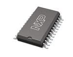
| 封装/外壳 | 24-SOIC(0.295",7.50mm 宽) |
| 封装/箱体 | SO-24 |
| 工作温度 | -40°C ~ 85°C |
| 工作温度范围 | - 40 C to + 85 C |
| 工作电源电压 | 2.3 V to 5.5 V |
| 工厂包装数量 | 1200 |
| 接口 | I²C, SMBus |
| 接口类型 | I2C, SMBus |
| 标准包装 | 30 |
| 特性 | POR |
| 特色产品 | http://www.digikey.com/cn/zh/ph/NXP/I2C.htmlhttp://www.digikey.cn/product-highlights/cn/zh/nxp-semiconductors-agile-i-o-gpio-expander/3040 |
| 电压-电源 | 2.3 V ~ 5.5 V |
| 电流-灌/拉输出 | 10mA, 25mA |
| 输出电流 | 50 mA |
| 输出类型 | 推挽式 |
| 逻辑系列 | PCA9555 |
| 零件号别名 | PCA9555D |
| 频率-时钟 | 400kHz |


- 商务部:美国ITC正式对集成电路等产品启动337调查
- 曝三星4nm工艺存在良率问题 高通将骁龙8 Gen1或转产台积电
- 太阳诱电将投资9.5亿元在常州建新厂生产MLCC 预计2023年完工
- 英特尔发布欧洲新工厂建设计划 深化IDM 2.0 战略
- 台积电先进制程称霸业界 有大客户加持明年业绩稳了
- 达到5530亿美元!SIA预计今年全球半导体销售额将创下新高
- 英特尔拟将自动驾驶子公司Mobileye上市 估值或超500亿美元
- 三星加码芯片和SET,合并消费电子和移动部门,撤换高东真等 CEO
- 三星电子宣布重大人事变动 还合并消费电子和移动部门
- 海关总署:前11个月进口集成电路产品价值2.52万亿元 增长14.8%


PDF Datasheet 数据手册内容提取
PCA9555 16-bit I2C-bus and SMBus I/O port with interrupt Rev. 10 — 8 November 2017 Product data sheet 1. General description The PCA9555 is a 24-pin CMOS device that provides 16bits of General Purpose parallel Input/Output (GPIO) expansion for I2C-bus/SMBus applications and was developed to enhance the NXPSemiconductors family of I2C-bus I/O expanders. The improvements include higher drive capability, 5V I/O tolerance, lower supply current, individual I/O configuration, and smaller packaging. I/O expanders provide a simple solution when additional I/O is needed for ACPI power switches, sensors, pushbuttons, LEDs, fans, etc. The PCA9555 consists of two 8-bit Configuration (Input or Output selection); Input, Output and Polarity Inversion (activeHIGH or activeLOW operation) registers. The system master can enable the I/Os as either inputs or outputs by writing to the I/O configuration bits. The data for each Input or Output is kept in the corresponding Input or Output register. The polarity of the read register can be inverted with the Polarity Inversion register. All registers can be read by the system master. Although pin-to-pin and I2C-bus address compatible with the PCF8575, software changes are required due to the enhancements, and are discussed in Application Note AN469. The PCA9555 open-drain interrupt output is activated when any input state differs from its corresponding input port register state and is used to indicate to the system master that an input state has changed. The power-on reset sets the registers to their default values and initializes the device state machine. Three hardware pins (A0, A1, A2) vary the fixed I2C-bus address and allow up to eight devices to share the same I2C-bus/SMBus. The fixed I2C-bus address of the PCA9555 is the same as the PCA9554, allowing up to eight of these devices in any combination to share the same I2C-bus/SMBus. 2. Features and benefits Operating power supply voltage range of 2.3V to 5.5V 5V tolerant I/Os Polarity Inversion register ActiveLOW interrupt output Low standby current Noise filter on SCL/SDA inputs No glitch on power-up Internal power-on reset 16 I/O pins which default to 16 inputs 0Hz to 400kHz clock frequency ESD protection exceeds 2000V HBM per JESD22-A114, 200V MM per JESD22-A115, and 1000V CDM per JESD22-C101
PCA9555 NXP Semiconductors 16-bit I2C-bus and SMBus I/O port with interrupt Latch-up testing is done to JEDEC Standard JESD78 which exceeds 100mA Five packages offered: SO24, SSOP24, TSSOP24, HVQFN24 and HWQFN24 3. Ordering information Table 1. Ordering info rmation Type number Topside mark Package Name Description Version PCA9555D PCA9555D SO24 plastic small outline package; 24leads; SOT137-1 bodywidth7.5mm PCA9555DB PCA9555 SSOP24 plastic shrink small outline package; 24leads; SOT340-1 bodywidth5.3mm PCA9555PW PCA9555 TSSOP24 plastic thin shrink small outline package; 24leads; SOT355-1 bodywidth4.4mm PCA9555BS 9555 HVQFN24 plastic thermal enhanced very thin quad flat package; SOT616-1 noleads; 24terminals; body440.85mm PCA9555HF P55H HWQFN24 plastic thermal enhanced veryvery thin quad flat SOT994-1 package; noleads; 24terminals; body440.75mm 3.1 Ordering options Table 2. Ordering opt ions Type number Orderable Package Packing method Minimum Temperature partnumber order quantity PCA9555D PCA9555D,112 SO24 STANDARD MARKING * IC'S 1200 T =40C to +85C amb TUBE - DSC BULK PACK PCA9555D,118 SO24 REEL 13" Q1/T1 *STANDARD 1000 MARK SMD PCA9555DB PCA9555DB,112 SSOP24 STANDARD MARKING * IC'S 826 T =40C to +85C amb TUBE - DSC BULK PACK PCA9555DB,118 SSOP24 REEL 13" Q1/T1 *STANDARD 1000 MARK SMD PCA9555PW PCA9555PW,112 TSSOP24 STANDARD MARKING * IC'S 1575 T =40C to +85C amb TUBE - DSC BULK PACK PCA9555PW,118 TSSOP24 REEL 13" Q1/T1 *STANDARD 2500 MARK SMD PCA9555BS PCA9555BS,118 HVQFN24 REEL 13" Q1/T1 *STANDARD 6000 T =40C to +85C amb MARK SMD PCA9555BSHP HVQFN24 REEL 13" Q2/T3 *STANDARD 6000 MARK SMD PCA9555HF PCA9555HF,118 HWQFN24 REEL 13" Q1/T1 *STANDARD 6000 T =40C to +85C amb MARK SMD PCA9555 All information provided in this document is subject to legal disclaimers. © NXP Semiconductors N.V. 2017. All rights reserved. Product data sheet Rev. 10 — 8 November 2017 2 of 34
PCA9555 NXP Semiconductors 16-bit I2C-bus and SMBus I/O port with interrupt 4. Block diagram PCA9555 IO1_0 IO1_1 A0 8-bit IO1_2 A1 INPUT/ IO1_3 OUTPUT A2 PORTS IO1_4 write pulse IO1_5 IO1_6 read pulse IO1_7 I2C-BUS/SMBus CONTROL SCL IO0_0 INPUT FILTER IO0_1 SDA 8-bit IO0_2 INPUT/ IO0_3 OUTPUT IO0_4 PORTS write pulse IO0_5 IO0_6 read pulse VDD POWER-ON IO0_7 RESET VSS VDD LP filter INT 002aac702 Remark: All I/Os are set to inputs at reset. Fig 1. Block diagram of PCA9555 5. Pinning information 5.1 Pinning INT 1 24 VDD A1 2 23 SDA A2 3 22 SCL IO0_0 4 21 A0 IO0_1 5 20 IO1_7 IO0_2 6 19 IO1_6 PCA9555D IO0_3 7 18 IO1_5 IO0_4 8 17 IO1_4 IO0_5 9 16 IO1_3 IO0_6 10 15 IO1_2 IO0_7 11 14 IO1_1 VSS 12 13 IO1_0 002aac698 Fig 2. Pin configuration for SO24 PCA9555 All information provided in this document is subject to legal disclaimers. © NXP Semiconductors N.V. 2017. All rights reserved. Product data sheet Rev. 10 — 8 November 2017 3 of 34
PCA9555 NXP Semiconductors 16-bit I2C-bus and SMBus I/O port with interrupt INT 1 24 VDD INT 1 24 VDD A1 2 23 SDA A1 2 23 SDA A2 3 22 SCL A2 3 22 SCL IO0_0 4 21 A0 IO0_0 4 21 A0 IO0_1 5 20 IO1_7 IO0_1 5 20 IO1_7 IO0_2 6 19 IO1_6 IO0_2 6 19 IO1_6 PCA9555DB PCA9555PW IO0_3 7 18 IO1_5 IO0_3 7 18 IO1_5 IO0_4 8 17 IO1_4 IO0_4 8 17 IO1_4 IO0_5 9 16 IO1_3 IO0_5 9 16 IO1_3 IO0_6 10 15 IO1_2 IO0_6 10 15 IO1_2 IO0_7 11 14 IO1_1 IO0_7 11 14 IO1_1 VSS 12 13 IO1_0 VSS 12 13 IO1_0 002aac699 002aac700 Fig 3. Pin configuration for SSOP24 Fig 4. Pin configuration for TSSOP24 itnedrmexin aarle 1a A2 A1 INT VDD SDA SCL itnedrmexin aarle 1a A2 A1 INT VDD SDA SCL 24 23 22 21 20 19 24 23 22 21 20 19 IO0_0 1 18 A0 IO0_0 1 18 A0 IO0_1 2 17 IO1_7 IO0_1 2 17 IO1_7 IO0_2 3 16 IO1_6 IO0_2 3 PCA9555HF 16 IO1_6 PCA9555BS IO0_3 4 15 IO1_5 IO0_3 4 15 IO1_5 IO0_4 5 14 IO1_4 IO0_4 5 14 IO1_4 IO0_5 6 13 IO1_3 IO0_5 6 13 IO1_3 7 8 9 10 11 12 7 8 9 10 11 12 O0_6 O0_7 VSS O1_0 O1_1 O1_2 002aac701 IO0_6 IO0_7 VSS IO1_0 IO1_1 IO1_2 002aac881 I I I I I Transparent top view Transparent top view Fig 5. Pin configuration for HVQFN24 Fig 6. Pin configuration for HWQFN24 PCA9555 All information provided in this document is subject to legal disclaimers. © NXP Semiconductors N.V. 2017. All rights reserved. Product data sheet Rev. 10 — 8 November 2017 4 of 34
PCA9555 NXP Semiconductors 16-bit I2C-bus and SMBus I/O port with interrupt 5.2 Pin description Table 3. Pin description Symbol Pin Description SO24, SSOP24, HVQFN24, TSSOP24 HWQFN24 INT 1 22 interrupt output (open-drain) A1 2 23 address input 1 A2 3 24 address input 2 IO0_0 4 1 port 0 input/output IO0_1 5 2 IO0_2 6 3 IO0_3 7 4 IO0_4 8 5 IO0_5 9 6 IO0_6 10 7 IO0_7 11 8 V 12 9[1] supply ground SS IO1_0 13 10 port 1 input/output IO1_1 14 11 IO1_2 15 12 IO1_3 16 13 IO1_4 17 14 IO1_5 18 15 IO1_6 19 16 IO1_7 20 17 A0 21 18 address input 0 SCL 22 19 serial clock line SDA 23 20 serial data line V 24 21 supply voltage DD [1] HVQFN and HWQFN package die supply ground is connected to both the V pin and the exposed center SS pad. The VSS pin must be connected to supply ground for proper device operation. For enhanced thermal, electrical, and board-level performance, the exposed pad needs to be soldered to the board using a corresponding thermal pad on the board, and for proper heat conduction through the board thermal vias need to be incorporated in the PCB in the thermal pad region. PCA9555 All information provided in this document is subject to legal disclaimers. © NXP Semiconductors N.V. 2017. All rights reserved. Product data sheet Rev. 10 — 8 November 2017 5 of 34
PCA9555 NXP Semiconductors 16-bit I2C-bus and SMBus I/O port with interrupt 6. Functional description Refer to Figure 1 “Block diagram of PCA9555”. 6.1 Device address slave address 0 1 0 0 A2 A1 A0 R/W fixed programmable 002aac219 Fig 7. PCA9555 device address 6.2 Registers 6.2.1 Command byte The command byte is the first byte to follow the address byte during a write transmission. It is used as a pointer to determine which of the following registers will be written or read. Table 4. Command byte Command Register 0 Input port0 1 Input port1 2 Output port0 3 Output port1 4 Polarity Inversion port0 5 Polarity Inversion port1 6 Configuration port0 7 Configuration port1 PCA9555 All information provided in this document is subject to legal disclaimers. © NXP Semiconductors N.V. 2017. All rights reserved. Product data sheet Rev. 10 — 8 November 2017 6 of 34
PCA9555 NXP Semiconductors 16-bit I2C-bus and SMBus I/O port with interrupt 6.2.2 Registers 0 and 1: Input port registers This register is an input-only port. It reflects the incoming logic levels of the pins, regardless of whether the pin is defined as an input or an output by Register3. Writes to this register have no effect. The default value ‘X’ is determined by the externally applied logic level. Table 5. Input port 0 Register Bit 7 6 5 4 3 2 1 0 Symbol I0.7 I0.6 I0.5 I0.4 I0.3 I0.2 I0.1 I0.0 Default X X X X X X X X Table 6. Input port 1 register Bit 7 6 5 4 3 2 1 0 Symbol I1.7 I1.6 I1.5 I1.4 I1.3 I1.2 I1.1 I1.0 Default X X X X X X X X 6.2.3 Registers 2 and 3: Output port registers This register is an output-only port. It reflects the outgoing logic levels of the pins defined as outputs by Registers 6 and 7. Bit values in this register have no effect on pins defined as inputs. In turn, reads from this register reflect the value that is in the flip-flop controlling the output selection, not the actual pin value. Table 7. Output port 0 register Bit 7 6 5 4 3 2 1 0 Symbol O0.7 O0.6 O0.5 O0.4 O0.3 O0.2 O0.1 O0.0 Default 1 1 1 1 1 1 1 1 Table 8. Output port 1 register Bit 7 6 5 4 3 2 1 0 Symbol O1.7 O1.6 O1.5 O1.4 O1.3 O1.2 O1.1 O1.0 Default 1 1 1 1 1 1 1 1 6.2.4 Registers 4 and 5: Polarity Inversion registers This register allows the user to invert the polarity of the Input port register data. If a bit in this register is set (written with ‘1’), the Input port data polarity is inverted. If a bit in this register is cleared (written with a ‘0’), the Input port data polarity is retained. Table 9. Polarity Inversion port 0 register Bit 7 6 5 4 3 2 1 0 Symbol N0.7 N0.6 N0.5 N0.4 N0.3 N0.2 N0.1 N0.0 Default 0 0 0 0 0 0 0 0 Table 10. Polarity Inversion port 1 register Bit 7 6 5 4 3 2 1 0 Symbol N1.7 N1.6 N1.5 N1.4 N1.3 N1.2 N1.1 N1.0 Default 0 0 0 0 0 0 0 0 PCA9555 All information provided in this document is subject to legal disclaimers. © NXP Semiconductors N.V. 2017. All rights reserved. Product data sheet Rev. 10 — 8 November 2017 7 of 34
PCA9555 NXP Semiconductors 16-bit I2C-bus and SMBus I/O port with interrupt 6.2.5 Registers 6 and 7: Configuration registers This register configures the directions of the I/O pins. If a bit in this register is set (written with ‘1’), the corresponding port pin is enabled as an input with high-impedance output driver. If a bit in this register is cleared (written with ‘0’), the corresponding port pin is enabled as an output. Note that there is a high value resistor tied to V at each pin. At DD reset, the device's ports are inputs with a pull-up to V . DD Table 11. Configuration port 0 register Bit 7 6 5 4 3 2 1 0 Symbol C0.7 C0.6 C0.5 C0.4 C0.3 C0.2 C0.1 C0.0 Default 1 1 1 1 1 1 1 1 Table 12. Configuration port 1 register Bit 7 6 5 4 3 2 1 0 Symbol C1.7 C1.6 C1.5 C1.4 C1.3 C1.2 C1.1 C1.0 Default 1 1 1 1 1 1 1 1 6.3 Power-on reset When power is applied to V , an internal power-on reset holds the PCA9555 in a reset DD condition until V has reached V . At that point, the reset condition is released and the DD POR PCA9555 registers and SMBus state machine will initialize to their default states. The power-on reset typically completes the reset and enables the part by the time the power supply is above V . However, when it is required to reset the part by lowering the power POR supply, it is necessary to lower it below 0.2V. 6.4 I/O port When an I/O is configured as an input, FETs Q1 and Q2 are off, creating a high-impedance input with a weak pull-up to V . The input voltage may be raised above DD V to a maximum of 5.5V. DD If the I/O is configured as an output, then either Q1 or Q2 is on, depending on the state of the Output Port register. Care should be exercised if an external voltage is applied to an I/O configured as an output because of the low-impedance path that exists between the pin and either V or V . DD SS PCA9555 All information provided in this document is subject to legal disclaimers. © NXP Semiconductors N.V. 2017. All rights reserved. Product data sheet Rev. 10 — 8 November 2017 8 of 34
PCA9555 NXP Semiconductors 16-bit I2C-bus and SMBus I/O port with interrupt data from output port shift register register data configuration register VDD data from D Q Q1 shift register FF 100 kΩ write D Q configuration CK Q pulse FF I/O pin write pulse CK Q2 output port input port VSS register register D Q input port FF register data read pulse CK to INT polarity inversion register data from D Q polarity shift register inversion FF register data write polarity CK pulse 002aac703 At power-on reset, all registers return to default values. Fig 8. Simplified schematic of I/Os 6.5 Bus transactions 6.5.1 Writing to the port registers Data is transmitted to the PCA9555 by sending the device address and setting the least significant bit to a logic0 (see Figure 7 “PCA9555 device address”). The command byte is sent after the address and determines which register will receive the data following the command byte. The eight registers within the PCA9555 are configured to operate as four register pairs. The four pairs are Input Ports, Output Ports, Polarity Inversion Ports, and Configuration Ports. After sending data to one register, the next data byte will be sent to the other register in the pair (see Figure9 and Figure10). For example, if the first byte is sent to Output Port 1 (register 3), then the next byte will be stored in Output Port 0 (register 2). There is no limitation on the number of data bytes sent in one write transmission. In this way, each 8-bit register may be updated independently of the other registers. PCA9555 All information provided in this document is subject to legal disclaimers. © NXP Semiconductors N.V. 2017. All rights reserved. Product data sheet Rev. 10 — 8 November 2017 9 of 34
xxxxxxxxxxxxxxxxxxxxx xxxxxxxxxxxxxxxxxxxxxxxxxx xxxxxxx x x x xxxxxxxxxxxxxxxxxxxxxxxxxxxxxx xxxxxxxxxxxxxxxxxxx xx xx xxxxx xxxxxxxxxxxxxxxxxxxxxxxxxxx xxxxxxxxxxxxxxxxxxx xxxxxx xxxxxxxxxxxxxxxxxxxxxxxxxxxxxxxxxxx xxxxxxxxxxxx x x xxxxxxxxxxxxxxxxxxxxx xxxxxxxxxxxxxxxxxxxxxxxxxxxxxx xxxxx xxxxxxxxxxxxxxxxxxxxxxxxxxxxxxxxxxxxxxxxxxxxxxxxxx xxxxxxxx xxxxxxxxxxxxxxxxxxxxxxxxx xxxxxxxxxxxxxxxxxxxx xxx P P N rodu CA9555 XP ct d SCL 1 2 3 4 5 6 7 8 9 S a e ta slave address command byte data to port 0 data to port 1 m sh ic e e SDA S 0 1 0 0 A2 A1 A0 0 A 0 0 0 0 0 0 1 0 A 0.7 DATA 0 0.0 A 1.7 DATA 1 1.0 A P o t n d START condition R/W acknowledge acknowledge acknowledge STOP u from slave from slave from slave condition c t o r s write to port tv(Q) data out from port 0 A tv(Q) ll inform fromda ptao rotu 1t DATA VALID Rev. 10 — 8 No ation provided in this docum Fig 9. Write to Outpu t port registers 002aac220 vember 2017 ent is subject to legal disclaimers. SSDCAL SSTA10RT 2c1osnl3da0ivtieo 4na0ddA5re2ssA61 A70R/8W0 9Aafrcokmn0 oswlalv0eedgce0omm0and0 byt1e 1 0 AafrcokMmnS osBwlalveedgdeataD tAoT rAeg 0ister LSB AafrcokMmnS osBwlalveedgdeataD tAoT rAeg 1ister LSB AcoSnTPdOitiPon 16-bit IC-bus2 a 002aac221 n d S Fig 10. Write to Configuration registers M B © N u XP Sem s I/O 10 of 34 iconductors N.V. 2017. All rights reserved. port with interrupt PCA9555
PCA9555 NXP Semiconductors 16-bit I2C-bus and SMBus I/O port with interrupt 6.5.2 Reading the port registers In order to read data from the PCA9555, the bus master must first send the PCA9555 address with the least significant bit set to a logic0 (see Figure 7 “PCA9555 device address”). The command byte is sent after the address and determines which register will be accessed. After a restart, the device address is sent again, but this time the least significant bit is set to a logic1. Data from the register defined by the command byte will then be sent by the PCA9555 (see Figure11, Figure12 and Figure13). Data is clocked into the register on the falling edge of the acknowledge clock pulse. After the first byte is read, additional bytes may be read but the data will now reflect the information in the other register in the pair. For example, if you read Input Port1, then the next byte read would be Input Port0. There is no limitation on the number of data bytes received in one read transmission but the final byte received, the bus master must not acknowledge the data. slave address SDA S 0 1 0 0 A2 A1 A0 0 A COMMAND BYTE A (cont.) START condition R/W acknowledge acknowledge from slave from slave data from lower or data from upper or upper byte of register lower byte of register slave address MSB LSB MSB LSB (cont.) S 0 1 0 0 A2 A1 A0 1 A DATA (first byte) A DATA (last byte) NA P (repeated) R/W acknowledge no acknowledge STOP START condition acknowledge from master from master condition from slave at this moment master-transmitter becomes master-receiver and slave-receiver becomes slave-transmitter 002aac222 Remark: Transfer can be stopped at any time by a STOP condition. Fig 11. Read from register PCA9555 All information provided in this document is subject to legal disclaimers. © NXP Semiconductors N.V. 2017. All rights reserved. Product data sheet Rev. 10 — 8 November 2017 11 of 34
xxxxxxxxxxxxxxxxxxxxx xxxxxxxxxxxxxxxxxxxxxxxxxx xxxxxxx x x x xxxxxxxxxxxxxxxxxxxxxxxxxxxxxx xxxxxxxxxxxxxxxxxxx xx xx xxxxx xxxxxxxxxxxxxxxxxxxxxxxxxxx xxxxxxxxxxxxxxxxxxx xxxxxx xxxxxxxxxxxxxxxxxxxxxxxxxxxxxxxxxxx xxxxxxxxxxxx x x xxxxxxxxxxxxxxxxxxxxx xxxxxxxxxxxxxxxxxxxxxxxxxxxxxx xxxxx xxxxxxxxxxxxxxxxxxxxxxxxxxxxxxxxxxxxxxxxxxxxxxxxxx xxxxxxxx xxxxxxxxxxxxxxxxxxxxxxxxx xxxxxxxxxxxxxxxxxxxx xxx P P N rodu CA9555 XP ct d data into port 0 S a e ta m she data into port 1 ic e o t n d IINNTT u c tv(INT_N) trst(INT_N) t o r s SCL 1 2 3 4 5 6 7 8 9 R/W STOP condition slave address I0.x I1.x I0.x I1.x SDA S 0 1 0 0 A2 A1 A0 1 A 7 6 5 4 3 2 1 0 A 7 6 5 4 3 2 1 0 AA 7 6 5 4 3 2 1 0 A 7 6 5 4 3 2 1 0 1 P A ll inform START condition acknowledge acknowledge acknowledge acknowledge non acknowledge Rev. 10 — 8 No ation provided in this docum rreeaadd ffrroomm ppoorrtt 01 from slave from master from master from master from ma0s0te2raac223 vember 2017 ent is subject to legal disclaimers. Fig 12. RRise eamasdsaur Ikmn:e pTdur atthn pastfo e trhrt eo r fc edogamitsam tcaeanrn,d s bbcey etsent ohaparpsioe pd r1 eavt iaonuys lmy boemeenn st ebty t ao S‘0T0O’ (Pre caodn Idniptiuotn P. Worht ereng tihstise ro).ccurs, data present at the latest acknowledge phase is valid (output mode). It 16-bit IC-bus2 a n d S M B © N u XP Sem s I/O 12 of 34 iconductors N.V. 2017. All rights reserved. port with interrupt PCA9555
xxxxxxxxxxxxxxxxxxxxx xxxxxxxxxxxxxxxxxxxxxxxxxx xxxxxxx x x x xxxxxxxxxxxxxxxxxxxxxxxxxxxxxx xxxxxxxxxxxxxxxxxxx xx xx xxxxx xxxxxxxxxxxxxxxxxxxxxxxxxxx xxxxxxxxxxxxxxxxxxx xxxxxx xxxxxxxxxxxxxxxxxxxxxxxxxxxxxxxxxxx xxxxxxxxxxxx x x xxxxxxxxxxxxxxxxxxxxx xxxxxxxxxxxxxxxxxxxxxxxxxxxxxx xxxxx xxxxxxxxxxxxxxxxxxxxxxxxxxxxxxxxxxxxxxxxxxxxxxxxxx xxxxxxxx xxxxxxxxxxxxxxxxxxxxxxxxx xxxxxxxxxxxxxxxxxxxx xxx P P N rodu CA9555 XP ct da data into port 0 DATA 00 th(D) DATA 01 DATA 02tsu(D) DATA 03 Se ta m shee data into port 1 DATA 10 th(D) DATA 11 tsu(D) DATA 12 ico t INT n d u tv(INT_N) trst(INT_N) c t o SCL 1 2 3 4 5 6 7 8 9 r s R/W STOP condition slave address I0.x I1.x I0.x I1.x SDA S 0 1 0 0 A2 A1 A0 1 A DATA 00 A DATA 10 AA DATA 03 A DATA 12 1 P A ll inform START condition ackfrnoomw lseldagvee afcrkonmo wmleadstgeer afcrkonmo wmleadstgeer afcrkonmo wmleadstgeer non afcrkonmo wmleadstgeer Rev. 10 — 8 No ation provided in this docum rreeaadd ffrroomm ppoorrtt 01 002aac224 vember 2017 ent is subject to legal disclaimers. Fig 13. RRise eamasdsaur Ikmn:e pTdur atthn pastfo etrhrt eo r fc edogamitsam tcaeanrn,d s bbcey etsent ohaparpsioe pd r2 eavt iaonuys lmy boemeenn st ebty t ao S‘0T0O’ (Pre caodn Idniptiuotn P. Worht ereng tihstise ro).ccurs, data present at the latest acknowledge phase is valid (output mode). It 16-bit IC-bus2 a n d S M B © N u XP Sem s I/O 13 of 34 iconductors N.V. 2017. All rights reserved. port with interrupt PCA9555
PCA9555 NXP Semiconductors 16-bit I2C-bus and SMBus I/O port with interrupt 6.5.3 Interrupt output The open-drain interrupt output is activated when one of the port pins changes state and the pin is configured as an input. The interrupt is deactivated when the input returns to its previous state or the Input Port register is read (see Figure12). A pin configured as an output cannot cause an interrupt. Since each 8-bit port is read independently, the interrupt caused by Port0 will not be cleared by a read of Port1 or the other way around. Remark: Changing an I/O from an output to an input may cause a false interrupt to occur if the state of the pin does not match the contents of the Input Port register. 7. Characteristics of the I2C-bus The I2C-bus is for 2-way, 2-line communication between different ICs or modules. The two lines are a serial data line (SDA) and a serial clock line (SCL). Both lines must be connected to a positive supply via a pull-up resistor when connected to the output stages of a device. Data transfer may be initiated only when the bus is not busy. 7.1 Bit transfer One data bit is transferred during each clock pulse. The data on the SDA line must remain stable during the HIGH period of the clock pulse as changes in the data line at this time will be interpreted as control signals (see Figure14). SDA SCL data line change stable; of data data valid allowed mba607 Fig 14. Bit transfer 7.1.1 START and STOP conditions Both data and clock lines remain HIGH when the bus is not busy. A HIGH-to-LOW transition of the data line while the clock is HIGH is defined as the START condition (S). A LOW-to-HIGH transition of the data line while the clock is HIGH is defined as the STOP condition (P) (see Figure15). SDA SCL S P START condition STOP condition mba608 Fig 15. Definition of START and STOP conditions PCA9555 All information provided in this document is subject to legal disclaimers. © NXP Semiconductors N.V. 2017. All rights reserved. Product data sheet Rev. 10 — 8 November 2017 14 of 34
PCA9555 NXP Semiconductors 16-bit I2C-bus and SMBus I/O port with interrupt 7.2 System configuration A device generating a message is a ‘transmitter’; a device receiving is the ‘receiver’. The device that controls the message is the ‘master’ and the devices which are controlled by the master are the ‘slaves’ (see Figure16). SDA SCL MASTER SLAVE SLAVE MASTER MASTER I2C-BUS TRANSMITTER/ RECEIVER TRANSMITTER/ TRANSMITTER TRANSMITTER/ MULTIPLEXER RECEIVER RECEIVER RECEIVER SLAVE 002aaa966 Fig 16. System configuration 7.3 Acknowledge The number of data bytes transferred between the START and the STOP conditions from transmitter to receiver is not limited. Each byte of eightbits is followed by one acknowledge bit. The acknowledge bit is a HIGH level put on the bus by the transmitter, whereas the master generates an extra acknowledge related clock pulse. A slave receiver which is addressed must generate an acknowledge after the reception of each byte. Also a master must generate an acknowledge after the reception of each byte that has been clocked out of the slave transmitter. The device that acknowledges has to pull down the SDA line during the acknowledge clock pulse, so that the SDA line is stable LOW during the HIGH period of the acknowledge related clock pulse; set-up time and hold time must be taken into account. A master receiver must signal an end of data to the transmitter by not generating an acknowledge on the last byte that has been clocked out of the slave. In this event, the transmitter must leave the data line HIGH to enable the master to generate a STOP condition. data output by transmitter not acknowledge data output by receiver acknowledge SCL from master 1 2 8 9 S clock pulse for START acknowledgement condition 002aaa987 Fig 17. Acknowledgement on the I2C-bus PCA9555 All information provided in this document is subject to legal disclaimers. © NXP Semiconductors N.V. 2017. All rights reserved. Product data sheet Rev. 10 — 8 November 2017 15 of 34
PCA9555 NXP Semiconductors 16-bit I2C-bus and SMBus I/O port with interrupt 8. Application design-in information VDD (5 V) SUB-SYSTEM 1 10 kΩ 10 kΩ 10 kΩ 2 kΩ (e.g., temp sensor) VDD VDD INT MASTER PCA9555 CONTROLLER SCL SCL IO0_0 SUB-SYSTEM 2 SDA SDA IO0_1 (e.g., counter) IO0_2 RESET INT INT IO0_3 A GND IO0_4 controlled ENABLE switch IO0_5 (e.g., CBT device) B IO0_6 IO0_7 SUB-SYSTEM 3 IO1_0 (e.g., alarm system) IO1_1 10 DIGIT IO1_2 NUMERIC ALARM IO1_3 KEYPAD IO1_4 A2 IO1_5 VDD A1 IO1_6 A0 IO1_7 VSS 002aac704 Device address configured as 0100000xb for this example. IO0_0, IO0_2, IO0_3 configured as outputs. IO0_1, IO0_4, IO0_5 configured as inputs. IO0_6, IO0_7, and IO1_0 to IO1_7 configured as inputs. Fig 18. Typical application PCA9555 All information provided in this document is subject to legal disclaimers. © NXP Semiconductors N.V. 2017. All rights reserved. Product data sheet Rev. 10 — 8 November 2017 16 of 34
PCA9555 NXP Semiconductors 16-bit I2C-bus and SMBus I/O port with interrupt 9. Limiting values Table 13. Limiting values In accordance with the Absolute Maximum Rating System (IEC 60134). Symbol Parameter Conditions Min Max Unit V supply voltage 0.5 +6.0 V DD V voltage on an input/output pin V 0.5 6 V I/O SS I output current on an I/O pin - 50 mA O I input current - 20 mA I I supply current - 160 mA DD I ground supply current - 200 mA SS P total power dissipation - 200 mW tot T storage temperature 65 +150 C stg T ambient temperature operating 40 +85 C amb T maximum junction - 125 C j(max) temperature PCA9555 All information provided in this document is subject to legal disclaimers. © NXP Semiconductors N.V. 2017. All rights reserved. Product data sheet Rev. 10 — 8 November 2017 17 of 34
PCA9555 NXP Semiconductors 16-bit I2C-bus and SMBus I/O port with interrupt 10. Static characteristics Table 14. Static charac teristics V =2.3V to 5.5V; V =0V; T =40C to +85C; unless otherwise specified. DD SS amb Symbol Parameter Conditions Min Typ Max Unit Supplies V supply voltage 2.3 - 5.5 V DD I supply current Operating mode; V =5.5V; noload; - 135 200 A DD DD f =100kHz SCL I standby current Standby mode; V =5.5V; noload; - 1.1 1.5 mA stb DD V =V ; f =0kHz; I/O=inputs I SS SCL Standby mode; V =5.5V; noload; - 0.25 1 A DD V =V ; f =0kHz; I/O=inputs I DD SCL V power-on reset voltage[1] no load; V =V or V - 1.7 2.2 V POR I DD SS Input SCL; input/output SDA V LOW-level input voltage 0.5 - +0.3V V IL DD V HIGH-level input voltage 0.7V - 5.5 V IH DD I LOW-level output current V =0.4V 3 - - mA OL OL I leakage current V =V =V 1 - +1 A L I DD SS C input capacitance V =V - 6 10 pF i I SS I/Os V LOW-level input voltage 0.5 - +0.3V V IL DD V HIGH-level input voltage 0.7V - 5.5 V IH DD I LOW-level output current V =2.3V to 5.5V; V =0.5V [2] 8 (8 to 20) - mA OL DD OL V =2.3V to 5.5V; V =0.7V [2] 10 (10to24) - mA DD OL V HIGH-level output voltage I =8mA; V =2.3V [3] 1.8 - - V OH OH DD I =10mA; V =2.3V [3] 1.7 - - V OH DD I =8mA; V =3.0V [3] 2.6 - - V OH DD I =10mA; V =3.0V [3] 2.5 - - V OH DD I =8mA; V =4.75V [3] 4.1 - - V OH DD I =10mA; V =4.75V [3] 4.0 - - V OH DD I HIGH-level input leakage V =5.5V; V =V - - 1 A LIH DD I DD current I LOW-level input leakage V =5.5V; V =V - - 100 A LIL DD I SS current C input capacitance - 3.7 5 pF i C output capacitance - 3.7 5 pF o Interrupt INT I LOW-level output current V =0.4V 3 - - mA OL OL Select inputs A0, A1, A2 V LOW-level input voltage 0.5 - +0.3V V IL DD V HIGH-level input voltage 0.7V - 5.5 V IH DD I input leakage current 1 - +1 A LI [1] VDD must be lowered to 0.2V for at least 5s in order to reset part. PCA9555 All information provided in this document is subject to legal disclaimers. © NXP Semiconductors N.V. 2017. All rights reserved. Product data sheet Rev. 10 — 8 November 2017 18 of 34
PCA9555 NXP Semiconductors 16-bit I2C-bus and SMBus I/O port with interrupt [2] Each I/O must be externally limited to a maximum of 25mA and each octal (IO0_0 to IO0_7 and IO1_0 to IO1_7) must be limited to a maximum current of 100mA for a device total of 200mA. [3] The total current sourced by all I/Os must be limited to 160mA. 002aac706 002aac707 6.0 4.5 V(VO)H VOH (V) 5.0 (1) 3.5 (2) 4.0 (1) 2.5 3.0 (2) 2.0 1.5 2.7 3.6 5.5 2.3 3.0 4.75 VDD (V) VDD (V) (1) IOH=8mA (1) IOH=8mA (2) IOH=10mA (2) IOH=10mA Fig 19. V maximum Fig 20. V minimum OH OH 002aac705 1.6 IDD (mA) (1) 1.2 (2) (3) 0.8 0.4 0 all 1s one 0 three 0s all 0s number of I/Os V =5.5V; V =5.5V; A2, A1, A0 set to logic0. DD I/O (1) Tamb=40C (2) Tamb=+25C (3) Tamb=+85C Fig 21. I versus number of I/Os held LOW DD PCA9555 All information provided in this document is subject to legal disclaimers. © NXP Semiconductors N.V. 2017. All rights reserved. Product data sheet Rev. 10 — 8 November 2017 19 of 34
PCA9555 NXP Semiconductors 16-bit I2C-bus and SMBus I/O port with interrupt 11. Dynamic characteristics Table 15. Dynamic cha racteristics Symbol Parameter Conditions Standard-mode Fast-mode I2C-bus Unit I2C-bus Min Max Min Max f SCL clock frequency 0 100 0 400 kHz SCL t bus free time between a STOP and 4.7 - 1.3 - s BUF START condition t hold time (repeated) START condition 4.0 - 0.6 - s HD;STA t set-up time for a repeated START 4.7 - 0.6 - s SU;STA condition t set-up time for STOP condition 4.0 - 0.6 - s SU;STO t data valid acknowledge time [1] 0.3 3.45 0.1 0.9 s VD;ACK t data hold time 0 - 0 - ns HD;DAT t data valid time [2] 300 - 50 - ns VD;DAT t data set-up time 250 - 100 - ns SU;DAT t LOW period of the SCL clock 4.7 - 1.3 - s LOW t HIGH period of the SCL clock 4.0 - 0.6 - s HIGH t fall time of both SDA and SCL signals - 300 20+0.1C [3] 300 ns f b t rise time of both SDA and SCL signals - 1000 20+0.1C [3] 300 ns r b t pulse width of spikes that must be - 50 - 50 ns SP suppressed by the input filter Port timing t data output valid time - 200 - 200 ns v(Q) t data input set-up time 150 - 150 - ns su(D) t data input hold time 1 - 1 - s h(D) Interrupt timing t valid time on pin INT - 4 - 4 s v(INT_N) t reset time on pin INT - 4 - 4 s rst(INT_N) [1] t =time for acknowledgement signal from SCL LOW to SDA (out) LOW. VD;ACK [2] t =minimum time for SDA data out to be valid following SCL LOW. VD;DAT [3] C =total capacitance of one bus line in pF. b PCA9555 All information provided in this document is subject to legal disclaimers. © NXP Semiconductors N.V. 2017. All rights reserved. Product data sheet Rev. 10 — 8 November 2017 20 of 34
PCA9555 NXP Semiconductors 16-bit I2C-bus and SMBus I/O port with interrupt 0.7 × VDD SDA 0.3 × VDD tBUF tr tf tHD;STA tSP tLOW 0.7 × VDD SCL 0.3 × VDD tHD;STA tSU;STA tSU;STO P S tHD;DAT tHIGH tSU;DAT Sr P 002aaa986 Fig 22. Definition of timing on the I2C-bus 12. Test information VDD open GND VDD RL 500 Ω VI VO PULSE DUT GENERATOR RT C50L pF 002aab284 R =load resistor. L C = load capacitance includes jig and probe capacitance. L RT = termination resistance should be equal to the output impedance of Zo of the pulse generators. Fig 23. Test circuitry for switching times RL S1 2VDD from output under test open 500 Ω GND CL RL 50 pF 500 Ω 002aac226 Fig 24. Load circuit PCA9555 All information provided in this document is subject to legal disclaimers. © NXP Semiconductors N.V. 2017. All rights reserved. Product data sheet Rev. 10 — 8 November 2017 21 of 34
PCA9555 NXP Semiconductors 16-bit I2C-bus and SMBus I/O port with interrupt 13. Package outline SO24: plastic small outline package; 24 leads; body width 7.5 mm SOT137-1 D E A X c y HE v M A Z 24 13 Q A2 A A1 (A 3 ) pin 1 index θ Lp L 1 12 detail X e w M bp 0 5 10 mm scale DIMENSIONS (inch dimensions are derived from the original mm dimensions) UNIT mAax. A1 A2 A3 bp c D(1) E(1) e HE L Lp Q v w y Z(1) θ 0.3 2.45 0.49 0.32 15.6 7.6 10.65 1.1 1.1 0.9 mm 2.65 0.25 1.27 1.4 0.25 0.25 0.1 0.1 2.25 0.36 0.23 15.2 7.4 10.00 0.4 1.0 0.4 8o 0.012 0.096 0.019 0.013 0.61 0.30 0.419 0.043 0.043 0.035 0o inches 0.1 0.01 0.05 0.055 0.01 0.01 0.004 0.004 0.089 0.014 0.009 0.60 0.29 0.394 0.016 0.039 0.016 Note 1. Plastic or metal protrusions of 0.15 mm (0.006 inch) maximum per side are not included. OUTLINE REFERENCES EUROPEAN ISSUE DATE VERSION IEC JEDEC JEITA PROJECTION 99-12-27 SOT137-1 075E05 MS-013 03-02-19 Fig 25. Package outline SOT137-1 (SO24) PCA9555 All information provided in this document is subject to legal disclaimers. © NXP Semiconductors N.V. 2017. All rights reserved. Product data sheet Rev. 10 — 8 November 2017 22 of 34
PCA9555 NXP Semiconductors 16-bit I2C-bus and SMBus I/O port with interrupt SSOP24: plastic shrink small outline package; 24 leads; body width 5.3 mm SOT340-1 D E A X c y HE v M A Z 24 13 Q A2 A1 (A 3 ) A pin 1 index θ Lp L 1 12 detail X w M e bp 0 2.5 5 mm scale DIMENSIONS (mm are the original dimensions) UNIT mAax. A1 A2 A3 bp c D(1) E(1) e HE L Lp Q v w y Z(1) θ mm 2 00..2015 11..8605 0.25 00..3285 00..2009 88..40 55..42 0.65 77..96 1.25 10..0633 00..97 0.2 0.13 0.1 00..84 80oo Note 1. Plastic or metal protrusions of 0.2 mm maximum per side are not included. OUTLINE REFERENCES EUROPEAN ISSUE DATE VERSION IEC JEDEC JEITA PROJECTION 99-12-27 SOT340-1 MO-150 03-02-19 Fig 26. Package outline SOT340-1 (SSOP24) PCA9555 All information provided in this document is subject to legal disclaimers. © NXP Semiconductors N.V. 2017. All rights reserved. Product data sheet Rev. 10 — 8 November 2017 23 of 34
PCA9555 NXP Semiconductors 16-bit I2C-bus and SMBus I/O port with interrupt TSSOP24: plastic thin shrink small outline package; 24 leads; body width 4.4 mm SOT355-1 D E A X c y HE v M A Z 24 13 Q A2 (A 3 ) A pin 1 index A1 θ Lp L 1 12 detail X w M e bp 0 2.5 5 mm scale DIMENSIONS (mm are the original dimensions) UNIT mAax. A1 A2 A3 bp c D(1) E(2) e HE L Lp Q v w y Z(1) θ 0.15 0.95 0.30 0.2 7.9 4.5 6.6 0.75 0.4 0.5 8o mm 1.1 0.05 0.80 0.25 0.19 0.1 7.7 4.3 0.65 6.2 1 0.50 0.3 0.2 0.13 0.1 0.2 0o Notes 1. Plastic or metal protrusions of 0.15 mm maximum per side are not included. 2. Plastic interlead protrusions of 0.25 mm maximum per side are not included. OUTLINE REFERENCES EUROPEAN ISSUE DATE VERSION IEC JEDEC JEITA PROJECTION 99-12-27 SOT355-1 MO-153 03-02-19 Fig 27. Package outline SOT355-1 (TSSOP24) PCA9555 All information provided in this document is subject to legal disclaimers. © NXP Semiconductors N.V. 2017. All rights reserved. Product data sheet Rev. 10 — 8 November 2017 24 of 34
PCA9555 NXP Semiconductors 16-bit I2C-bus and SMBus I/O port with interrupt HVQFN24: plastic thermal enhanced very thin quad flat package; no leads; 24 terminals; body 4 x 4 x 0.85 mm SOT616-1 D B A terminal 1 index area A A1 E c detail X e1 C 1/2 e e b v M C A B y1 C y 7 12 w M C L 13 6 e Eh e2 1/2 e 1 18 terminal 1 index area 24 19 Dh X 0 2.5 5 mm scale DIMENSIONS (mm are the original dimensions) A(1) UNIT max. A1 b c D(1) Dh E(1) Eh e e1 e2 L v w y y1 0.05 0.30 4.1 2.25 4.1 2.25 0.5 mm 1 0.2 0.5 2.5 2.5 0.1 0.05 0.05 0.1 0.00 0.18 3.9 1.95 3.9 1.95 0.3 Note 1. Plastic or metal protrusions of 0.075 mm maximum per side are not included. OUTLINE REFERENCES EUROPEAN ISSUE DATE VERSION IEC JEDEC JEITA PROJECTION 01-08-08 SOT616-1 - - - MO-220 - - - 02-10-22 Fig 28. Package outline SOT616-1 (HVQFN24) PCA9555 All information provided in this document is subject to legal disclaimers. © NXP Semiconductors N.V. 2017. All rights reserved. Product data sheet Rev. 10 — 8 November 2017 25 of 34
PCA9555 NXP Semiconductors 16-bit I2C-bus and SMBus I/O port with interrupt HWQFN24: plastic thermal enhanced very very thin quad flat package; no leads; 24 terminals; body 4 x 4 x 0.75 mm SOT994-1 D B A terminal 1 index area E A A1 c detail X e1 1/2 e C ∅ v M C A B e b ∅ wM C y1C y 7 12 L 13 6 e Eh e2 1/2 e 1 18 terminal 1 index area 24 19 X Dh 0 2.5 5 mm scale DIMENSIONS (mm are the original dimensions) UNIT mA(a1x) A1 b c D(1) Dh E(1) Eh e e1 e2 L v w y y1 0.05 0.30 4.1 2.25 4.1 2.25 0.5 mm 0.8 0.2 0.5 2.5 2.5 0.1 0.05 0.05 0.1 0.00 0.18 3.9 1.95 3.9 1.95 0.3 Note 1. Plastic or metal protrusions of 0.075 mm maximum per side are not included. OUTLINE REFERENCES EUROPEAN ISSUE DATE VERSION IEC JEDEC JEITA PROJECTION 07-02-07 SOT994-1 - - - MO-220 - - - 07-03-03 Fig 29. Package outline SOT994-1 (HWQFN24) PCA9555 All information provided in this document is subject to legal disclaimers. © NXP Semiconductors N.V. 2017. All rights reserved. Product data sheet Rev. 10 — 8 November 2017 26 of 34
PCA9555 NXP Semiconductors 16-bit I2C-bus and SMBus I/O port with interrupt 14. Handling information All input and output pins are protected against ElectroStatic Discharge (ESD) under normal handling. When handling ensure that the appropriate precautions are taken as described in JESD625-A or equivalent standards. 15. Soldering of SMD packages This text provides a very brief insight into a complex technology. A more in-depth account of soldering ICs can be found in Application Note AN10365 “Surface mount reflow soldering description”. 15.1 Introduction to soldering Soldering is one of the most common methods through which packages are attached to Printed Circuit Boards (PCBs), to form electrical circuits. The soldered joint provides both the mechanical and the electrical connection. There is no single soldering method that is ideal for all IC packages. Wave soldering is often preferred when through-hole and Surface Mount Devices (SMDs) are mixed on one printed wiring board; however, it is not suitable for fine pitch SMDs. Reflow soldering is ideal for the small pitches and high densities that come with increased miniaturization. 15.2 Wave and reflow soldering Wave soldering is a joining technology in which the joints are made by solder coming from a standing wave of liquid solder. The wave soldering process is suitable for the following: • Through-hole components • Leaded or leadless SMDs, which are glued to the surface of the printed circuit board Not all SMDs can be wave soldered. Packages with solder balls, and some leadless packages which have solder lands underneath the body, cannot be wave soldered. Also, leaded SMDs with leads having a pitch smaller than ~0.6mm cannot be wave soldered, due to an increased probability of bridging. The reflow soldering process involves applying solder paste to a board, followed by component placement and exposure to a temperature profile. Leaded packages, packages with solder balls, and leadless packages are all reflow solderable. Key characteristics in both wave and reflow soldering are: • Board specifications, including the board finish, solder masks and vias • Package footprints, including solder thieves and orientation • The moisture sensitivity level of the packages • Package placement • Inspection and repair • Lead-free soldering versus SnPb soldering 15.3 Wave soldering Key characteristics in wave soldering are: PCA9555 All information provided in this document is subject to legal disclaimers. © NXP Semiconductors N.V. 2017. All rights reserved. Product data sheet Rev. 10 — 8 November 2017 27 of 34
PCA9555 NXP Semiconductors 16-bit I2C-bus and SMBus I/O port with interrupt • Process issues, such as application of adhesive and flux, clinching of leads, board transport, the solder wave parameters, and the time during which components are exposed to the wave • Solder bath specifications, including temperature and impurities 15.4 Reflow soldering Key characteristics in reflow soldering are: • Lead-free versus SnPb soldering; note that a lead-free reflow process usually leads to higher minimum peak temperatures (see Figure30) than a SnPb process, thus reducing the process window • Solder paste printing issues including smearing, release, and adjusting the process window for a mix of large and small components on one board • Reflow temperature profile; this profile includes preheat, reflow (in which the board is heated to the peak temperature) and cooling down. It is imperative that the peak temperature is high enough for the solder to make reliable solder joints (a solder paste characteristic). In addition, the peak temperature must be low enough that the packages and/or boards are not damaged. The peak temperature of the package depends on package thickness and volume and is classified in accordance with Table16 and17 Table 16. SnPb eutectic process (from J-STD-020C) Package thickness (mm) Package reflow temperature (C) Volume (mm3) < 350 350 < 2.5 235 220 2.5 220 220 Table 17. Lead-free process (from J-STD-020C) Package thickness (mm) Package reflow temperature (C) Volume (mm3) < 350 350 to 2000 > 2000 < 1.6 260 260 260 1.6 to 2.5 260 250 245 > 2.5 250 245 245 Moisture sensitivity precautions, as indicated on the packing, must be respected at all times. Studies have shown that small packages reach higher temperatures during reflow soldering, see Figure30. PCA9555 All information provided in this document is subject to legal disclaimers. © NXP Semiconductors N.V. 2017. All rights reserved. Product data sheet Rev. 10 — 8 November 2017 28 of 34
PCA9555 NXP Semiconductors 16-bit I2C-bus and SMBus I/O port with interrupt maximum peak temperature = MSL limit, damage level temperature minimum peak temperature = minimum soldering temperature peak temperature time 001aac844 MSL: Moisture Sensitivity Level Fig 30. Temperature profiles for large and small components For further information on temperature profiles, refer to Application Note AN10365 “Surface mount reflow soldering description”. 16. Soldering of through-hole mount packages 16.1 Introduction to soldering through-hole mount packages This text gives a very brief insight into wave, dip and manual soldering. Wave soldering is the preferred method for mounting of through-hole mount IC packages on a printed-circuit board. 16.2 Soldering by dipping or by solder wave Driven by legislation and environmental forces the worldwide use of lead-free solder pastes is increasing. Typical dwell time of the leads in the wave ranges from 3secondsto4seconds at 250C or 265C, depending on solder material applied, SnPb or Pb-free respectively. The total contact time of successive solder waves must not exceed 5seconds. The device may be mounted up to the seating plane, but the temperature of the plastic body must not exceed the specified maximum storage temperature (T ). If the stg(max) printed-circuit board has been pre-heated, forced cooling may be necessary immediately after soldering to keep the temperature within the permissible limit. 16.3 Manual soldering Apply the soldering iron (24V or less) to the lead(s) of the package, either below the seating plane or not more than 2mm above it. If the temperature of the soldering iron bit is less than 300C it may remain in contact for up to 10seconds. If the bit temperature is between 300Cand400C, contact may be up to 5seconds. PCA9555 All information provided in this document is subject to legal disclaimers. © NXP Semiconductors N.V. 2017. All rights reserved. Product data sheet Rev. 10 — 8 November 2017 29 of 34
PCA9555 NXP Semiconductors 16-bit I2C-bus and SMBus I/O port with interrupt 16.4 Package related soldering information Table 18. Suitability of through-hole mount IC packages for dipping and wave soldering Package Soldering method Dipping Wave CPGA, HCPGA - suitable DBS, DIP, HDIP, RDBS, SDIP, SIL suitable suitable[1] PMFP[2] - not suitable [1] For SDIP packages, the longitudinal axis must be parallel to the transport direction of the printed-circuit board. [2] For PMFP packages hot bar soldering or manual soldering is suitable. 17. Abbreviations Table 19. Abbreviations Acronym Description CMOS Complementary Metal Oxide Semiconductor GPIO General Purpose Input/Output I2C-bus Inter-Integrated Circuit bus SMBus System Management Bus I/O Input/Output ACPI Advanced Configuration and Power Interface LED Light Emitting Diode ESD ElectroStatic Discharge HBM Human Body Model MM Machine Model CDM Charged Device Model PCB Printed-Circuit Board FET Field-Effect Transistor MSB Most Significant Bit LSB Least Significant Bit PCA9555 All information provided in this document is subject to legal disclaimers. © NXP Semiconductors N.V. 2017. All rights reserved. Product data sheet Rev. 10 — 8 November 2017 30 of 34
PCA9555 NXP Semiconductors 16-bit I2C-bus and SMBus I/O port with interrupt 18. Revision history Table 20. Revision history Document ID Release date Data sheet status Change notice Supersedes PCA9555 v.10 20171108 Product data sheet 201710002I PCA9555_9 Modifications: • Table 14 “Static characteristics”: Corrected V typ and max limit POR • Added Section 3.1 “Ordering options” • Obsolete part PCA9555N (DIP24, SOT101-1) removed PCA9555 v.9 20170510 Product data sheet - PCA9555_8 Modifications: • Table 13 “Limiting values”, added row for T j(max) PCA9555_8 20091022 Product data sheet - PCA9555_7 Modifications: • Table 2 “Ordering options”, Topside mark for TSSOP24 package, PCA9555PW, is changed from “PCA9555PW” to “PCA9555” • Figure 12 “Read Input port register, scenario 1” modified • Figure 13 “Read Input port register, scenario 2” modified • Table 14 “Static characteristics”, Table note [1] modified (added phrase “for at least 5s”) • updated soldering information PCA9555_7 20070605 Product data sheet - PCA9555_6 PCA9555_6 20060825 Product data sheet - PCA9555_5 PCA9555_5 20040930 Product data sheet - PCA9555_4 (939775014125) PCA9555_4 20040727 Product data sheet - PCA9555_3 (939775013271) PCA9555_3 20020726 Product data 853-225228672 of PCA9555_2 (939775010164) 2002July26 PCA9555_2 20020513 Product data - PCA9555_1 (939775009818) PCA9555_1 20010507 Product data - - (939775008343) PCA9555 All information provided in this document is subject to legal disclaimers. © NXP Semiconductors N.V. 2017. All rights reserved. Product data sheet Rev. 10 — 8 November 2017 31 of 34
PCA9555 NXP Semiconductors 16-bit I2C-bus and SMBus I/O port with interrupt 19. Legal information 19.1 Data sheet status Document status[1][2] Product status[3] Definition Objective [short] data sheet Development This document contains data from the objective specification for product development. Preliminary [short] data sheet Qualification This document contains data from the preliminary specification. Product [short] data sheet Production This document contains the product specification. [1] Please consult the most recently issued document before initiating or completing a design. [2] The term ‘short data sheet’ is explained in section “Definitions”. [3] The product status of device(s) described in this document may have changed since this document was published and may differ in case of multiple devices. The latest product status information is available on the Internet at URLhttp://www.nxp.com. 19.2 Definitions Suitability for use — NXP Semiconductors products are not designed, authorized or warranted to be suitable for use in life support, life-critical or safety-critical systems or equipment, nor in applications where failure or Draft — The document is a draft version only. The content is still under malfunction of an NXP Semiconductors product can reasonably be expected internal review and subject to formal approval, which may result in to result in personal injury, death or severe property or environmental modifications or additions. NXP Semiconductors does not give any damage. NXP Semiconductors and its suppliers accept no liability for representations or warranties as to the accuracy or completeness of inclusion and/or use of NXP Semiconductors products in such equipment or information included herein and shall have no liability for the consequences of applications and therefore such inclusion and/or use is at the customer’s own use of such information. risk. Short data sheet — A short data sheet is an extract from a full data sheet Applications — Applications that are described herein for any of these with the same product type number(s) and title. A short data sheet is intended products are for illustrative purposes only. NXP Semiconductors makes no for quick reference only and should not be relied upon to contain detailed and representation or warranty that such applications will be suitable for the full information. For detailed and full information see the relevant full data specified use without further testing or modification. sheet, which is available on request via the local NXP Semiconductors sales office. In case of any inconsistency or conflict with the short data sheet, the Customers are responsible for the design and operation of their applications full data sheet shall prevail. and products using NXP Semiconductors products, and NXP Semiconductors accepts no liability for any assistance with applications or customer product Product specification — The information and data provided in a Product design. It is customer’s sole responsibility to determine whether the NXP data sheet shall define the specification of the product as agreed between Semiconductors product is suitable and fit for the customer’s applications and NXP Semiconductors and its customer, unless NXP Semiconductors and products planned, as well as for the planned application and use of customer have explicitly agreed otherwise in writing. In no event however, customer’s third party customer(s). Customers should provide appropriate shall an agreement be valid in which the NXP Semiconductors product is design and operating safeguards to minimize the risks associated with their deemed to offer functions and qualities beyond those described in the applications and products. Product data sheet. NXP Semiconductors does not accept any liability related to any default, damage, costs or problem which is based on any weakness or default in the 19.3 Disclaimers customer’s applications or products, or the application or use by customer’s third party customer(s). Customer is responsible for doing all necessary testing for the customer’s applications and products using NXP Limited warranty and liability — Information in this document is believed to Semiconductors products in order to avoid a default of the applications and be accurate and reliable. However, NXP Semiconductors does not give any the products or of the application or use by customer’s third party representations or warranties, expressed or implied, as to the accuracy or customer(s). NXP does not accept any liability in this respect. completeness of such information and shall have no liability for the consequences of use of such information. NXP Semiconductors takes no Limiting values — Stress above one or more limiting values (as defined in responsibility for the content in this document if provided by an information the Absolute Maximum Ratings System of IEC60134) will cause permanent source outside of NXP Semiconductors. damage to the device. Limiting values are stress ratings only and (proper) operation of the device at these or any other conditions above those given in In no event shall NXP Semiconductors be liable for any indirect, incidental, the Recommended operating conditions section (if present) or the punitive, special or consequential damages (including - without limitation - lost Characteristics sections of this document is not warranted. Constant or profits, lost savings, business interruption, costs related to the removal or repeated exposure to limiting values will permanently and irreversibly affect replacement of any products or rework charges) whether or not such the quality and reliability of the device. damages are based on tort (including negligence), warranty, breach of contract or any other legal theory. Terms and conditions of commercial sale — NXP Semiconductors products are sold subject to the general terms and conditions of commercial Notwithstanding any damages that customer might incur for any reason whatsoever, NXP Semiconductors’ aggregate and cumulative liability towards sale, as published at http://www.nxp.com/profile/terms, unless otherwise customer for the products described herein shall be limited in accordance agreed in a valid written individual agreement. In case an individual with the Terms and conditions of commercial sale of NXP Semiconductors. agreement is concluded only the terms and conditions of the respective agreement shall apply. NXP Semiconductors hereby expressly objects to Right to make changes — NXP Semiconductors reserves the right to make applying the customer’s general terms and conditions with regard to the changes to information published in this document, including without purchase of NXP Semiconductors products by customer. limitation specifications and product descriptions, at any time and without notice. This document supersedes and replaces all information supplied prior No offer to sell or license — Nothing in this document may be interpreted or to the publication hereof. construed as an offer to sell products that is open for acceptance or the grant, conveyance or implication of any license under any copyrights, patents or other industrial or intellectual property rights. PCA9555 All information provided in this document is subject to legal disclaimers. © NXP Semiconductors N.V. 2017. All rights reserved. Product data sheet Rev. 10 — 8 November 2017 32 of 34
PCA9555 NXP Semiconductors 16-bit I2C-bus and SMBus I/O port with interrupt Export control — This document as well as the item(s) described herein whenever customer uses the product for automotive applications beyond may be subject to export control regulations. Export might require a prior NXP Semiconductors’ specifications such use shall be solely at customer’s authorization from competent authorities. own risk, and (c) customer fully indemnifies NXP Semiconductors for any liability, damages or failed product claims resulting from customer design and Quick reference data — The Quick reference data is an extract of the use of the product for automotive applications beyond NXP Semiconductors’ product data given in the Limiting values and Characteristics sections of this standard warranty and NXP Semiconductors’ product specifications. document, and as such is not complete, exhaustive or legally binding. Translations — A non-English (translated) version of a document is for Non-automotive qualified products — Unless this data sheet expressly reference only. The English version shall prevail in case of any discrepancy states that this specific NXP Semiconductors product is automotive qualified, between the translated and English versions. the product is not suitable for automotive use. It is neither qualified nor tested in accordance with automotive testing or application requirements. NXP Semiconductors accepts no liability for inclusion and/or use of 19.4 Trademarks non-automotive qualified products in automotive equipment or applications. In the event that customer uses the product for design-in and use in Notice: All referenced brands, product names, service names and trademarks automotive applications to automotive specifications and standards, customer are the property of their respective owners. (a) shall use the product without NXP Semiconductors’ warranty of the I2C-bus — logo is a trademark of NXP Semiconductors N.V. product for such automotive applications, use and specifications, and (b) 20. Contact information For more information, please visit: http://www.nxp.com For sales office addresses, please send an email to: salesaddresses@nxp.com PCA9555 All information provided in this document is subject to legal disclaimers. © NXP Semiconductors N.V. 2017. All rights reserved. Product data sheet Rev. 10 — 8 November 2017 33 of 34
PCA9555 NXP Semiconductors 16-bit I2C-bus and SMBus I/O port with interrupt 21. Contents 1 General description. . . . . . . . . . . . . . . . . . . . . . 1 17 Abbreviations . . . . . . . . . . . . . . . . . . . . . . . . . 30 2 Features and benefits . . . . . . . . . . . . . . . . . . . . 1 18 Revision history . . . . . . . . . . . . . . . . . . . . . . . 31 3 Ordering information. . . . . . . . . . . . . . . . . . . . . 2 19 Legal information . . . . . . . . . . . . . . . . . . . . . . 32 3.1 Ordering options. . . . . . . . . . . . . . . . . . . . . . . . 2 19.1 Data sheet status. . . . . . . . . . . . . . . . . . . . . . 32 4 Block diagram . . . . . . . . . . . . . . . . . . . . . . . . . . 3 19.2 Definitions . . . . . . . . . . . . . . . . . . . . . . . . . . . 32 19.3 Disclaimers . . . . . . . . . . . . . . . . . . . . . . . . . . 32 5 Pinning information. . . . . . . . . . . . . . . . . . . . . . 3 19.4 Trademarks . . . . . . . . . . . . . . . . . . . . . . . . . . 33 5.1 Pinning . . . . . . . . . . . . . . . . . . . . . . . . . . . . . . . 3 5.2 Pin description . . . . . . . . . . . . . . . . . . . . . . . . . 5 20 Contact information . . . . . . . . . . . . . . . . . . . . 33 6 Functional description . . . . . . . . . . . . . . . . . . . 6 21 Contents. . . . . . . . . . . . . . . . . . . . . . . . . . . . . . 34 6.1 Device address. . . . . . . . . . . . . . . . . . . . . . . . . 6 6.2 Registers . . . . . . . . . . . . . . . . . . . . . . . . . . . . . 6 6.2.1 Command byte. . . . . . . . . . . . . . . . . . . . . . . . . 6 6.2.2 Registers 0 and 1: Input port registers. . . . . . . 7 6.2.3 Registers 2 and 3: Output port registers. . . . . . 7 6.2.4 Registers 4 and 5: Polarity Inversion registers. 7 6.2.5 Registers 6 and 7: Configuration registers. . . . 8 6.3 Power-on reset. . . . . . . . . . . . . . . . . . . . . . . . . 8 6.4 I/O port . . . . . . . . . . . . . . . . . . . . . . . . . . . . . . . 8 6.5 Bus transactions. . . . . . . . . . . . . . . . . . . . . . . . 9 6.5.1 Writing to the port registers. . . . . . . . . . . . . . . . 9 6.5.2 Reading the port registers . . . . . . . . . . . . . . . 11 6.5.3 Interrupt output. . . . . . . . . . . . . . . . . . . . . . . . 14 7 Characteristics of the I2C-bus . . . . . . . . . . . . 14 7.1 Bit transfer . . . . . . . . . . . . . . . . . . . . . . . . . . . 14 7.1.1 START and STOP conditions. . . . . . . . . . . . . 14 7.2 System configuration . . . . . . . . . . . . . . . . . . . 15 7.3 Acknowledge . . . . . . . . . . . . . . . . . . . . . . . . . 15 8 Application design-in information . . . . . . . . . 16 9 Limiting values. . . . . . . . . . . . . . . . . . . . . . . . . 17 10 Static characteristics. . . . . . . . . . . . . . . . . . . . 18 11 Dynamic characteristics. . . . . . . . . . . . . . . . . 20 12 Test information. . . . . . . . . . . . . . . . . . . . . . . . 21 13 Package outline. . . . . . . . . . . . . . . . . . . . . . . . 22 14 Handling information. . . . . . . . . . . . . . . . . . . . 27 15 Soldering of SMD packages . . . . . . . . . . . . . . 27 15.1 Introduction to soldering. . . . . . . . . . . . . . . . . 27 15.2 Wave and reflow soldering. . . . . . . . . . . . . . . 27 15.3 Wave soldering. . . . . . . . . . . . . . . . . . . . . . . . 27 15.4 Reflow soldering. . . . . . . . . . . . . . . . . . . . . . . 28 16 Soldering of through-hole mount packages. 29 16.1 Introduction to soldering through-hole mount packages . . . . . . . . . . . . . . . . . . . . . . . . . . . . 29 16.2 Soldering by dipping or by solder wave . . . . . 29 16.3 Manual soldering . . . . . . . . . . . . . . . . . . . . . . 29 16.4 Package related soldering information. . . . . . 30 Please be aware that important notices concerning this document and the product(s) described herein, have been included in section ‘Legal information’. © NXP Semiconductors N.V. 2017. All rights reserved. For more information, please visit: http://www.nxp.com For sales office addresses, please send an email to: salesaddresses@nxp.com Date of release: 8 November 2017 Document identifier: PCA9555
Mouser Electronics Authorized Distributor Click to View Pricing, Inventory, Delivery & Lifecycle Information: N XP: PCA9555BS,118 PCA9555D,112 PCA9555DB,112 PCA9555DB,118 PCA9555D,118 PCA9555HF,118 PCA9555N,112 PCA9555PW,112 PCA9555PW/DG,118 PCA9555PW,118 PCA9555BSHP