ICGOO在线商城 > 集成电路(IC) > 接口 - I/O 扩展器 > PCA9534ARGTR
 Datasheet下载
- 型号: PCA9534ARGTR
- 制造商: Texas Instruments
- 库位|库存: xxxx|xxxx
- 要求:
| 数量阶梯 | 香港交货 | 国内含税 |
| +xxxx | $xxxx | ¥xxxx |
查看当月历史价格
查看今年历史价格
PCA9534ARGTR产品简介:
ICGOO电子元器件商城为您提供PCA9534ARGTR由Texas Instruments设计生产,在icgoo商城现货销售,并且可以通过原厂、代理商等渠道进行代购。 PCA9534ARGTR价格参考¥5.04-¥11.35。Texas InstrumentsPCA9534ARGTR封装/规格:接口 - I/O 扩展器, I/O Expander 8 I²C, SMBus 400kHz 16-QFN (3x3)。您可以下载PCA9534ARGTR参考资料、Datasheet数据手册功能说明书,资料中有PCA9534ARGTR 详细功能的应用电路图电压和使用方法及教程。
Texas Instruments(德州仪器)的PCA9534ARGTR是一款I²C兼容的8位I/O扩展器,广泛应用于需要扩展GPIO(通用输入/输出)接口的场景。以下是其主要应用场景:

 1. 嵌入式系统控制
   - 在嵌入式系统中,主控制器(如微控制器或微处理器)可能缺乏足够的GPIO引脚来连接外部设备。PCA9534ARGTR可以扩展多达8个额外的GPIO引脚,用于驱动LED、按键、继电器或其他外围设备。
   - 常见应用包括家用电器、工业控制器和消费电子产品。

 2. LED驱动与状态指示
   - PCA9534ARGTR可用于驱动多个LED,作为状态指示灯。通过I²C总线控制,可以灵活调整LED的开关状态和亮度。
   - 例如,在工业设备中,使用不同颜色的LED指示运行状态、故障报警等。

 3. 按键与开关检测
   - 该芯片可连接多个按键或开关,将输入信号通过I²C接口传输到主控芯片。适用于遥控器、键盘、面板按钮等需要多路输入的应用。
   - 在家电或医疗设备中,用于检测用户操作。

 4. 继电器与电机控制
   - 通过GPIO引脚驱动晶体管或MOSFET,PCA9534ARGTR可以控制继电器或小型电机的开关状态。适用于自动化设备、安防系统等。

 5. 传感器数据采集
   - 在物联网(IoT)或环境监测系统中,PCA9534ARGTR可以用作传感器接口,采集数字信号并通过I²C总线传输给主控制器。
   - 支持连接温度传感器、湿度传感器、光敏传感器等多种数字输入设备。

 6. 电源管理与监控
   - 在电源管理系统中,PCA9534ARGTR可用于监控电源状态、控制电源开关或管理电池充电电路。
   - 例如,在便携式设备中,用于检测电池电压或控制省电模式。

 7. 多路复用与简化设计
   - 在复杂的电子系统中,PCA9534ARGTR可以减少主控芯片的引脚占用,简化PCB布线设计,降低开发成本。
   - 特别适合需要多路I/O扩展但空间有限的场合。

 总结
PCA9534ARGTR凭借其低功耗、小封装(SOT-23-14)、宽工作电压范围(1.7V至5.5V)以及I²C接口的灵活性,成为许多嵌入式系统和工业应用的理想选择。它广泛应用于消费电子、工业自动化、通信设备、医疗设备等领域,为开发者提供了高效、可靠的I/O扩展解决方案。
| 参数 | 数值 |
| 产品目录 | 集成电路 (IC)半导体 |
| 描述 | IC I/O EXPANDER I2C 8B 16VQFN接口-I/O扩展器 Remote 8B I2C and Lo-Pwr I/O Expander |
| 产品分类 | |
| I/O数 | 8 |
| 品牌 | Texas Instruments |
| 产品手册 | |
| 产品图片 |
|
| rohs | 符合RoHS无铅 / 符合限制有害物质指令(RoHS)规范要求 |
| 产品系列 | 接口 IC,接口-I/O扩展器,Texas Instruments PCA9534ARGTR- |
| 数据手册 | |
| 产品型号 | PCA9534ARGTR |
| PCN设计/规格 | |
| 中断输出 | 是 |
| 产品目录页面 | |
| 产品种类 | 接口-I/O扩展器 |
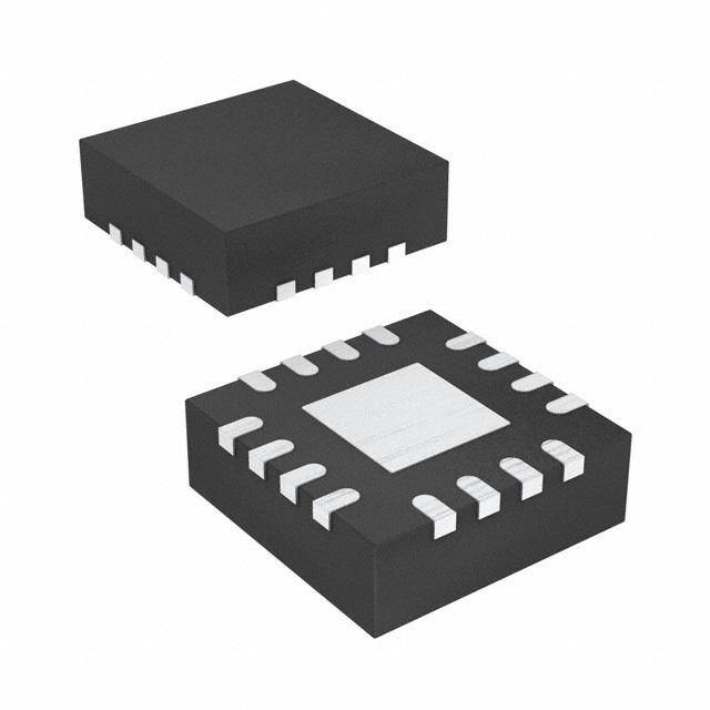
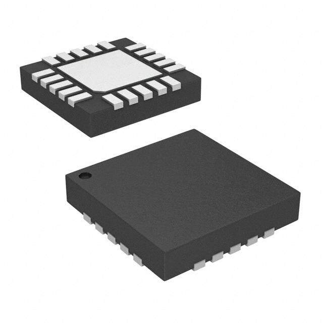
| 供应商器件封装 | 16-QFN(3x3) |
| 其它名称 | 296-24731-2 |
| 包装 | 带卷 (TR) |
| 单位重量 | 24.100 mg |
| 商标 | Texas Instruments |
| 安装类型 | 表面贴装 |
| 安装风格 | SMD/SMT |
| 封装 | Reel |
| 封装/外壳 | 16-VFQFN 裸露焊盘 |
| 封装/箱体 | VQFN-16 |
| 工作温度 | -40°C ~ 85°C |
| 工作温度范围 | - 40 C to + 85 C |
| 工作电源电压 | 2.3 V to 5.5 V |
| 工厂包装数量 | 3000 |
| 接口 | I²C, SMBus |
| 最大工作频率 | 400 kHz |
| 标准包装 | 3,000 |
| 特性 | POR |
| 电压-电源 | 2.3 V ~ 5.5 V |
| 电流-灌/拉输出 | 10mA, 25mA |
| 系列 | PCA9534A |
| 输入/输出端数量 | 8 I/O |
| 输出类型 | 推挽式 |
| 逻辑系列 | PCA9534A |
| 频率-时钟 | 400kHz |


.jpg)


- 商务部:美国ITC正式对集成电路等产品启动337调查
- 曝三星4nm工艺存在良率问题 高通将骁龙8 Gen1或转产台积电
- 太阳诱电将投资9.5亿元在常州建新厂生产MLCC 预计2023年完工
- 英特尔发布欧洲新工厂建设计划 深化IDM 2.0 战略
- 台积电先进制程称霸业界 有大客户加持明年业绩稳了
- 达到5530亿美元!SIA预计今年全球半导体销售额将创下新高
- 英特尔拟将自动驾驶子公司Mobileye上市 估值或超500亿美元
- 三星加码芯片和SET,合并消费电子和移动部门,撤换高东真等 CEO
- 三星电子宣布重大人事变动 还合并消费电子和移动部门
- 海关总署:前11个月进口集成电路产品价值2.52万亿元 增长14.8%


PDF Datasheet 数据手册内容提取
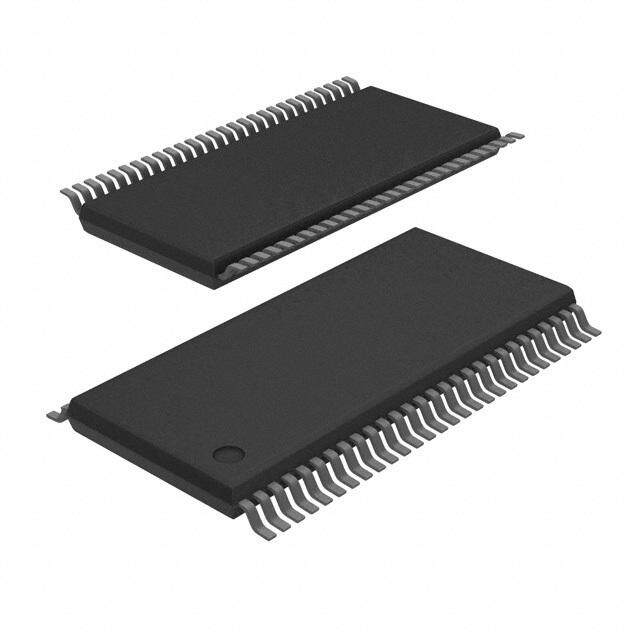
Product Sample & Technical Tools & Support & Folder Buy Documents Software Community PCA9534A SCPS141I–SEPTEMBER2006–REVISEDJUNE2014 2 PCA9534A Remote 8-BIT I C and SMBus Low-Power I/O Expander With Interrupt Output And Configuration Registers 1 Features 2 Description • LowStandbyCurrentConsumptionof1μAMax This 8-bit I/O expander for the two-line bidirectional 1 bus (I2C) is designed for 2.3-V to 5.5-V V • I2CtoParallelPortExpander CC operation. It provides general-purpose remote I/O • Open-DrainActive-LowInterruptOutput expansionformostmicrocontrollerfamiliesviatheI2C • OperatingPower-SupplyVoltageRangeof2.3V interface[serialclock(SCL),serialdata(SDA)]. to5.5V The PCA9534A consists of one 8-bit configuration • 5-VTolerantI/OPorts (input or output selection), input port, output port, and • 400-kHzFastI2CBus polarity inversion (active high or active low) register. At power on, the I/Os are configured as inputs. • ThreeHardwareAddressPinsAllowUptoEight However, the system master can enable the I/Os as DevicesontheI2C/SMBus either inputs or outputs by writing to the I/O • AllowsUpto16DevicesontheI2C/SMBusWhen configuration bits. The data for each input or output is UsedinConjunctionwiththePCA9534 keptinthecorrespondinginputoroutputregister.The SeeDeviceComparisonTableforI2CExpander polarity of the input port register can be inverted with offerings the polarity inversion register. All registers can be readbythesystemmaster. • Input/OutputConfigurationRegister • PolarityInversionRegister The system master can reset the PCA9534A in the event of a timeout or other improper operation by • InternalPower-OnReset utilizing the power-on reset feature, which puts the • Power-UpWithAllChannelsConfiguredasInputs registers in their default state and initializes the • NoGlitchonPower-Up I2C/SMBusstatemachine. • NoiseFilteronSCL/SDAInputs The PCA9534A open-drain interrupt (INT) output is • LatchedOutputsWithHigh-CurrentDrive activated when any input state differs from its corresponding input port register state and is used to MaximumCapabilityforDirectlyDrivingLEDs indicate to the system master that an input state has • Latch-UpPerformanceExceeds100mAPer changed. JESD78,ClassII The PCA9534A and PCA9534 are identical, except • ESDProtectionExceedsJESD22 for their fixed I2C address. This allows for up to 16 of – 2000-VHuman-BodyModel(A114-A) thesedevices(8ofeach)onthesameI2Cbus. – 200-VMachineModel(A115-A) DeviceInformation(1) – 1000-VCharged-DeviceModel(C101) PARTNUMBER PACKAGE BODYSIZE(NOM) SSOP(16) 6.20mm×5.30mm PCA9534A VQFN(16) 4.00mm×4.00mm QFN(16) 3.00mm×3.00mm (1) For all available packages, see the orderable addendum at theendofthedatasheet. DB, DBQ, DGV, DW, OR PW PACKAGE RGV PACKAGE RGT PACKAGE (TOPVIEW) (TOPVIEW) (TOPVIEW) A1 A0 VCC SDA A10AVCCDSA A0 1 16 VCC 16 15 14 13 161514 13 A1 2 15 SDA A2 1 12 SCL A2 1 12 SCL A2 3 14 SCL P0 2 11 INT P0 2 11 INT P0 4 13 INT P1 3 10 P7 P1 5 12 P7 P1 3 10 P7 P2 4 9 P6 P2 6 11 P6 P2 4 9 P6 5 6 7 8 P3 7 10 P5 5 6 7 8 P3NDP4 P5 GND 8 9 P4 3 D 4 5 G P N P P G 1 An IMPORTANT NOTICE at the end of this data sheet addresses availability, warranty, changes, use in safety-critical applications, intellectualpropertymattersandotherimportantdisclaimers.PRODUCTIONDATA.
PCA9534A SCPS141I–SEPTEMBER2006–REVISEDJUNE2014 www.ti.com Table of Contents 1 Features.................................................................. 1 9 DetailedDescription............................................ 15 2 Description............................................................. 1 9.1 FunctionalBlockDiagram.......................................15 3 RevisionHistory..................................................... 2 9.2 DeviceFunctionalModes........................................16 4 Description(Continued)........................................ 3 9.3 Programming...........................................................17 5 DeviceComparisonTable..................................... 4 10 ApplicationAndImplementation....................... 24 10.1 TypicalApplication ...............................................24 6 PinConfigurationandFunctions......................... 5 11 PowerSupplyRecommendations..................... 26 7 Specifications......................................................... 6 11.1 Power-OnResetRequirements ...........................26 7.1 AbsoluteMaximumRatings .....................................6 11.2 Power-OnResetErrata.........................................27 7.2 HandlingRatings.......................................................6 12 DeviceandDocumentationSupport................. 28 7.3 RecommendedOperatingConditions.......................6 7.4 ElectricalCharacteristics...........................................7 12.1 Trademarks...........................................................28 7.5 I2CInterfaceTimingRequirements...........................8 12.2 ElectrostaticDischargeCaution............................28 7.6 SwitchingCharacteristics..........................................8 12.3 Glossary................................................................28 7.7 TypicalCharacteristics..............................................9 13 Mechanical,Packaging,andOrderable Information........................................................... 28 8 ParameterMeasurementInformation................12 3 Revision History ChangesfromRevisionH(June2010)toRevisionI Page • RemovedOrderingInformationTable.................................................................................................................................... 4 • AddedInterruptErratasection............................................................................................................................................. 17 • Deletedthe100kΩresistoratV ....................................................................................................................................... 24 CC • AddedPower-OnResetErratasection................................................................................................................................ 27 2 SubmitDocumentationFeedback Copyright©2006–2014,TexasInstrumentsIncorporated ProductFolderLinks:PCA9534A
PCA9534A www.ti.com SCPS141I–SEPTEMBER2006–REVISEDJUNE2014 4 Description (Continued) INT can be connected to the interrupt input of a microcontroller. By sending an interrupt signal on this line, the remote I/O can inform the microcontroller if there is incoming data on its ports without having to communicate via theI2Cbus.Thus,thePCA9534Acanremainasimpleslavedevice. The device's outputs (latched) have high-current drive capability for directly driving LEDs. It has low current consumption. Three hardware pins (A0, A1, and A2) are used to program and vary the fixed I2C address and allow up to eight devicestosharethesameI2CbusorSMBus. The PCA9534A is pin-to-pin and I2C address compatible with the PCF8574A. However, software changes are requiredduetotheenhancementsinthePCA9534AoverthePCF8574A. The PCA9534A is a low-power version of the PCA9554A. The only difference between the PCA9534A and PCA9554A is that the PCA9534A eliminates an internal I/O pullup resistor, which dramatically reduces power consumptioninthestandbymodewhentheI/Osareheldlow. Copyright©2006–2014,TexasInstrumentsIncorporated SubmitDocumentationFeedback 3 ProductFolderLinks:PCA9534A
PCA9534A SCPS141I–SEPTEMBER2006–REVISEDJUNE2014 www.ti.com 5 Device Comparison Table DEVICE FRMEAQXUE ADI2DCRE RAVNCCGE NGOP.IOOsF INTPETRRU RINEPSUETT CONFIGNURATIO TO5L-VER PPUUSLHL- ODRPEANIN- COMMENT NCY SS OUTPUT REGISTERS ANT I/OTYPE I/OTYPE TCA6408 400 0100 1.65to5.5 8 Yes Yes Yes Yes Yes No Poweronreset,tf(falltime)>100msand 00x tr(ramptime)<10ms Unrestrictedpoweronresetramp/falltime. 0100 TCA6408 400 00x 1.65to5.5 8 Yes Yes Yes Yes Yes No Bothtf(falltime)andTRT(ramptime)can bebetween0.1msand2000ms TCA6416 400 0100 1.65to5.5 16 Yes Yes Yes Yes Yes No Poweronreset,tf(falltime)>100msand 00x TRT(ramptime)<10ms Unrestrictedpoweronresetramp/falltime. TCA6416 0100 A 400 00x 1.65to5.5 16 Yes Yes Yes Yes Yes No Bothtf(falltime)andTRT(ramptime)can bebetween0.1msand2000ms TCA6424 400 0100 1.65to5.5 24 Yes Yes Yes Yes Yes No Poweronreset,tf(falltime)>100msand 00x TRT(ramptime)<10ms 0100 TCA9535 400 1.65to5.5 16 Yes No Yes Yes Yes No xxx 1110 TCA9539 400 1.65to5.5 16 Yes Yes Yes Yes Yes No 1xx 0100 TCA9555 400 1.65to5.5 16 Yes No Yes Yes Yes No xxx Yes Oneopendrainoutput;eightpushpull 0011 Yes PCA6107 400 2.3to5.5 8 Yes Yes Yes Yes P1―P7 outputs xxx P0bit bits PCA9534hasadifferentslaveaddressas PCA9534 400 0100 2.3to5.5 8 Yes No Yes Yes Yes No thePCA9534A,allowingupto16devices xxx '9534typedevicesonthesameI2Cbus PCA9534Ahasadifferentslaveaddress PCA9534 0111 asthePCA9534,allowingupto16 A 400 xxx 2.3to5.5 8 Yes No Yes Yes Yes No devices'9534typedevicesonthesame I2Cbus 0100 PCA9535 400 2.3to5.5 16 Yes No Yes Yes Yes No xxx 1000 PCA9536 400 2.3to5.5 4 No No Yes Yes Yes No 001 1110 PCA9538 400 2.3to5.5 8 Yes Yes Yes Yes Yes No 0xx 1110 PCA9539 400 2.3to5.5 16 Yes Yes Yes Yes Yes No 1xx 0100 PCA9554 400 2.3to5.5 8 Yes No Yes Yes Yes No xxx PCA9554 0111 400 2.3to5.5 8 Yes No Yes Yes Yes No A xxx 0100 PCA9555 400 2.3to5.5 16 Yes No Yes Yes Yes No xxx 0011 PCA9557 400 2.3to5.5 8 No Yes Yes Yes Yes Yes xxx PCA8574hasadifferentslaveaddressas PCF8574 400 0100 2.5to6.0 8 Yes No No Yes Yes No thePCA8574A,allowingupto16devices xxx '9534typedevicesonthesameI2Cbus PCA8574Ahasadifferentslaveaddress PCF8574 0111 asthePCA8574,allowingupto16 A 400 xxx 2.5to6.0 8 Yes No No Yes Yes No devices'9534typedevicesonthesame I2Cbus 0100 PCF8575 400 2.5to5.5 16 Yes No No Yes Yes No xxx PCF8575 0100 400 4.5to5.5 16 Yes No No Yes No Yes C xxx 4 SubmitDocumentationFeedback Copyright©2006–2014,TexasInstrumentsIncorporated ProductFolderLinks:PCA9534A
PCA9534A www.ti.com SCPS141I–SEPTEMBER2006–REVISEDJUNE2014 6 Pin Configuration and Functions DB, DBQ, DGV, DW, OR PW PACKAGE RGV PACKAGE RGT PACKAGE (TOPVIEW) (TOPVIEW) (TOPVIEW) A1 A0 VCC SDA A1 0A VCCDSA A0 1 16 VCC 16 15 14 13 16 15 14 13 A1 2 15 SDA A2 1 12 SCL A2 1 12 SCL A2 3 14 SCL P0 2 11 INT P0 2 11 INT P0 4 13 INT P1 3 10 P7 P1 3 10 P7 P1 5 12 P7 P2 4 9 P6 P2 6 11 P6 P2 4 9 P6 5 6 7 8 P3 7 10 P5 5 6 7 8 3 D 4 5 P N P P GND 8 9 P4 3 D 4 5 G P N P P G PinFunctions PIN QSOP(DBQ), SOIC(DW), QFN(RGT) DESCRIPTION NAME SSOP(DB), AND TSSOP(PW),AND QFN(RGV) TVSOP(DGV) A0 1 15 Addressinput.ConnectdirectlytoV orground. CC A1 2 16 Addressinput.ConnectdirectlytoV orground. CC A2 3 1 Addressinput.ConnectdirectlytoV orground. CC P0 4 2 P-portinput/output.Push-pulldesignstructure. P1 5 3 P-portinput/output.Push-pulldesignstructure. P2 6 4 P-portinput/output.Push-pulldesignstructure. P3 7 5 P-portinput/output.Push-pulldesignstructure. GND 8 6 Ground P4 9 7 P-portinput/output.Push-pulldesignstructure. P5 10 8 P-portinput/output.Push-pulldesignstructure. P6 11 9 P-portinput/output.Push-pulldesignstructure. P7 12 10 P-portinput/output.Push-pulldesignstructure. INT 13 11 Interruptoutput.ConnecttoV throughapullupresistor. CC SCL 14 12 Serialclockbus.ConnecttoV throughapullupresistor. CC SDA 15 13 Serialdatabus.ConnecttoV throughapullupresistor. CC V 16 14 Supplyvoltage CC Copyright©2006–2014,TexasInstrumentsIncorporated SubmitDocumentationFeedback 5 ProductFolderLinks:PCA9534A
PCA9534A SCPS141I–SEPTEMBER2006–REVISEDJUNE2014 www.ti.com 7 Specifications 7.1 Absolute Maximum Ratings(1) overoperatingfree-airtemperaturerange(unlessotherwisenoted) MIN MAX UNIT V Supplyvoltagerange –0.5 6 V CC V Inputvoltagerange(2) –0.5 6 V I V Outputvoltagerange(2) –0.5 6 V O I Inputclampcurrent V <0 –20 mA IK I I Outputclampcurrent V <0 –20 mA OK O I Input/outputclampcurrent V <0orV >V ±20 mA IOK O O CC I Continuousoutputlowcurrent V =0toV 50 mA OL O CC I Continuousoutputhighcurrent V =0toV –50 mA OH O CC ContinuouscurrentthroughGND –250 I mA CC ContinuouscurrentthroughV 160 CC DBpackage 82 DBQpackage 90 DGVpackage 86 DWpackage 46 θ Packagethermalimpedance(3) °C/W JA Npackage 67 PWpackage 88 RGTpackage TBD RGVpackage 51 (1) Stressesbeyondthoselistedunder"absolutemaximumratings"maycausepermanentdamagetothedevice.Thesearestressratings only,andfunctionaloperationofthedeviceattheseoranyotherconditionsbeyondthoseindicatedunder"recommendedoperating conditions"isnotimplied.Exposuretoabsolute-maximum-ratedconditionsforextendedperiodsmayaffectdevicereliability. (2) Theinputnegative-voltageandoutputvoltageratingsmaybeexceedediftheinputandoutputcurrentratingsareobserved. (3) ThepackagethermalimpedanceiscalculatedinaccordancewithJESD51-7. 7.2 Handling Ratings MIN MAX UNIT T Storagetemperaturerange –65 150 °C stg Humanbodymodel(HBM),perANSI/ESDA/JEDECJS-001,all pins(1) 0 2000 V Electrostaticdischarge V (ESD) Chargeddevicemodel(CDM),perJEDECspecification JESD22-C101,allpins(2) 0 1000 (1) JEDECdocumentJEP155statesthat500-VHBMallowssafemanufacturingwithastandardESDcontrolprocess. (2) JEDECdocumentJEP157statesthat250-VCDMallowssafemanufacturingwithastandardESDcontrolprocess. 7.3 Recommended Operating Conditions MIN MAX UNIT V Supplyvoltage 2.3 5.5 V CC SCL,SDA 0.7×V 5.5 CC V High-levelinputvoltage V IH A2–A0,P7–P0 2 5.5 SCL,SDA –0.5 0.3×V CC V Low-levelinputvoltage V IL A2–A0,P7–P0 –0.5 0.8 I High-leveloutputcurrent P7–P0 –10 mA OH I Low-leveloutputcurrent P7–P0 25 mA OL T Operatingfree-airtemperature –40 85 °C A 6 SubmitDocumentationFeedback Copyright©2006–2014,TexasInstrumentsIncorporated ProductFolderLinks:PCA9534A
PCA9534A www.ti.com SCPS141I–SEPTEMBER2006–REVISEDJUNE2014 7.4 Electrical Characteristics overoperatingfree-airtemperaturerange(unlessotherwisenoted) PARAMETER TESTCONDITIONS V MIN TYP(1) MAX UNIT CC V Inputdiodeclampvoltage I =–18mA 2.3Vto5.5V –1.2 V IK I V Power-onresetvoltage V =V orGND,I =0 V 1.5 1.65 V POR I CC O POR 2.3V 1.8 3V 2.6 I =–8mA OH 4.5V 4.1 4.75V 4.1 V P-porthigh-leveloutputvoltage(2) V OH 2.3V 1.7 3V 2.5 I =–10mA OH 4.5V 4 4.75V 4 SDA V =0.4V 2.3Vto5.5V 3 8 OL 2.3V 8 10 3V 8 14 V =0.5V OL 4.5V 8 17 4.75V 8 35 I Pport(3) mA OL 2.3V 10 13 3V 10 19 V =0.7V OL 4.5V 10 24 4.75V 10 45 INT V =0.4V 2.3Vto5.5V 3 10 OL SCL,SDA ±1 I V =V orGND 2.3Vto5.5V μA I I CC A2–A0 ±1 I Pport V =V 2.3Vto5.5V 1 μA IH I CC I Pport V =GND 2.3Vto5.5V –1 μA IL I 5.5V 104 175 V =V orGND,I =0, I CC O 3.6V 50 90 I/O=inputs,f =400kHz scl 2.7V 20 65 Operatingmode 5.5V 60 150 V =V orGND,I =0, I I CC O 3.6V 15 40 μA CC I/O=inputs,f =100kHz scl 2.7V 8 20 5.5V 0.25 1 V =GND,I =0, Standbymode I O 3.6V 0.2 0.9 I/O=inputs,f =0kHz scl 2.7V 0.1 0.8 OneinputatV –0.6V, CC 2.3Vto5.5V 1.5 Additionalcurrentinstandby OtherinputsatVCCorGND ΔI mA CC mode AllLEDI/OsatV =4.3V, I 5.5V 1 f =0kHz scl C SCL V =V orGND 2.3Vto5.5V 4 5 pF I I CC SDA 5.5 6.5 C V =V orGND 2.3Vto5.5V pF io IO CC Pport 8 9.5 (1) Alltypicalvaluesareatnominalsupplyvoltage(2.5-V,3.3-V,or5-VV )andT =25°C. CC A (2) ThetotalcurrentsourcedbyallI/Osmustbelimitedto85mA. (3) EachI/Omustbeexternallylimitedtoamaximumof25mA,andthePport(P7–P0)mustbelimitedtoamaximumcurrentof200mA. Copyright©2006–2014,TexasInstrumentsIncorporated SubmitDocumentationFeedback 7 ProductFolderLinks:PCA9534A
PCA9534A SCPS141I–SEPTEMBER2006–REVISEDJUNE2014 www.ti.com 7.5 I2C Interface Timing Requirements overoperatingfree-airtemperaturerange(unlessotherwisenoted)(seeFigure14) STANDARDMODE FASTMODE I2CBUS I2CBUS UNIT MIN MAX MIN MAX f I2Cclockfrequency 0 100 0 400 kHz scl t I2Cclockhightime 4 0.6 μs sch t I2Cclocklowtime 4.7 1.3 μs scl t I2Cspiketime 50 50 ns sp t I2Cserial-datasetuptime 250 100 ns sds t I2Cserial-dataholdtime 0 0 ns sdh t I2Cinputrisetime 1000 20+0.1C (1) 300 ns icr b t I2Cinputfalltime 300 20+0.1C (1) 300 ns icf b t I2Coutputfalltime 10-pFto400-pFbus 300 20+0.1C (1) 300 ns ocf b t I2Cbusfreetimebetweenstopandstart 4.7 1.3 μs buf t I2Cstartorrepeatedstartconditionsetup 4.7 0.6 μs sts t I2Cstartorrepeatedstartconditionhold 4 0.6 μs sth t I2Cstopconditionsetup 4 0.6 μs sps t Validdatatime SCLlowtoSDAoutputvalid 300 50 ns vd(data) ACKsignalfromSCLlowto t ValiddatatimeofACKcondition 0.3 3.45 0.1 0.9 μs vd(ack) SDA(out)low C I2Cbuscapacitiveload 400 400 ns b (1) C =totalcapacitiveofonebusinpF b 7.6 Switching Characteristics overoperatingfree-airtemperaturerange(unlessotherwisenoted)(seeFigure15andFigure16) STANDARDMODE FASTMODE PARAMETER FROM TO I2CBUS I2CBUS UNIT (INPUT) (OUTPUT) MIN MAX MIN MAX t Interruptvalidtime Pport INT 4 4 μs iv t Interruptresetdelaytime SCL INT 4 4 μs ir t Outputdatavalid SCL P7–P0 200 200 ns pv t Inputdatasetuptime Pport SCL 100 100 ns ps t Inputdataholdtime Pport SCL 1 1 μs ph 8 SubmitDocumentationFeedback Copyright©2006–2014,TexasInstrumentsIncorporated ProductFolderLinks:PCA9534A
PCA9534A www.ti.com SCPS141I–SEPTEMBER2006–REVISEDJUNE2014 7.7 Typical Characteristics 55 35 50 VCC=5V 30 45 µA 40 nA 25 VCC=5V urrent– 3305 fI/SOCLs=u4n0lo0akdHezd urrent– 20 VCC=3.3V C C Supply 2205 VCC=3.3V Supply 15 VCC=2.5V – 15 – 10 ICC 10 VCC=2.5V ICC 5 5 SCL=VCC 0 0 -40 -15 10 35 60 85 -40 -15 10 35 60 85 TA–Free-AirTemperature–°C TA–Free-AirTemperature–°C Figure1.SupplyCurrentvsTemperature Figure2.QuiescentSupplyCurrentvsTemperature 70 600 fI/SOCLs=u4n0lo0akdHezd 550 VCC=5V 60 500 I–SupplyCurrent–µACC 23450000 I–SupplyCurrent–µACC 122334450505050000000 TA=25T°CA=–40°C TA=85°C 100 10 50 0 0 0 1 2 3 4 5 6 7 8 2.3 2.7 3.1 3.5 3.9 4.3 4.7 5.1 5.5 NumberofI/OsHeldLow VCC–SupplyVoltage–V Figure4.SupplyCurrentvsNumberOfI/OsHeldLow Figure3.SupplyCurrentvsSupplyVoltage 300 30 275 VCC=2.5V 250 VCC=2.5V,ISINK=10mA 25 –mV 225 mA TA=–40°C wVoltage 112570050 VCC=5V,ISINK=10mA Current– 1250 TA=25°C V–OutputLoOL 1157020505 VCC=2.5V,ISINK=1mAVCC=5V,ISINK=1mA I–I/OSinkSINK 150 TA=85°C 25 0 0 -40 -15 10 35 60 85 0.0 0.1 0.2 0.3 0.4 0.5 0.6 0.7 TA–Free-AirTemperature–°C VOL–OutputLowVoltage–V Figure5.I/OOutputLowVoltagevsTemperature Figure6.I/OSinkCurrentvsOutputLowVoltage Copyright©2006–2014,TexasInstrumentsIncorporated SubmitDocumentationFeedback 9 ProductFolderLinks:PCA9534A
PCA9534A SCPS141I–SEPTEMBER2006–REVISEDJUNE2014 www.ti.com Typical Characteristics (continued) 40 60 VCC=3.3V 55 VCC=5V 35 TA=–40°C 50 mA 30 mA 45 nt– 25 nt– 40 TA=–40°C Curre 20 TA=25°C Curre 3305 TA=25°C k k n n Si Si 25 –I/O 15 TA=85°C –I/O 20 TA=85°C ISINK 10 ISINK 1105 5 5 0 0 0.0 0.1 0.2 0.3 0.4 0.5 0.6 0.7 0.0 0.1 0.2 0.3 0.4 0.5 0.6 0.7 VOL–OutputLowVoltage–V VOL–OutputLowVoltage–V Figure7.I/OSinkCurrentvsOutputLowVoltage Figure8.I/OSinkCurrentvsOutputLowVoltage 275 35 250 VCC=2.5V hVoltage–mV 122702505 VCC=2.5V,IOL=10mA Current–mA 223050 TA=25°C TA=–40°C putHig 112550 VCC=5V,IOL=10mA Source 15 ut O –O 100 –I/ 10 (V–V)CCOH 257505 VCC=2.5V,IOL=1mA VCC=5V,IOL=1mA ISOURCE 05 TA=85°C 0 0.0 0.1 0.2 0.3 0.4 0.5 0.6 0.7 -40 -15 10 35 60 85 (VCC–VOH)–OutputHighVoltage–V TA–Free-AirTemperature–°C Figure10.I/OSourceCurrentvsOutputHighVoltage Figure9.I/OOutputHighVoltagevsTemperature 50 75 45 VCC=3.3V 70 VCC=5V 65 mA 40 mA 60 Current– 3305 TA=25°CTA=–40°C Current– 455505 TA=–40°C urce 25 urce 3450 TA=25°C o o S 20 S 30 –I/O 15 TA=85°C –I/O 2205 TA=85°C ISOURCE 150 ISOURCE 1105 5 0 0 0.0 0.1 0.2 0.3 0.4 0.5 0.6 0.7 0.0 0.1 0.2 0.3 0.4 0.5 0.6 0.7 (VCC–VOH)–OutputHighVoltage–V (VCC–VOH)–OutputHighVoltage–V Figure11.I/OSourceCurrentvsOutputHighVoltage Figure12.I/OSourceCurrentvsOutputHighVoltage 10 SubmitDocumentationFeedback Copyright©2006–2014,TexasInstrumentsIncorporated ProductFolderLinks:PCA9534A
PCA9534A www.ti.com SCPS141I–SEPTEMBER2006–REVISEDJUNE2014 Typical Characteristics (continued) 6 TA=25°C 5 V – e ag 4 Volt IOH=–8mA h Hig 3 ut Outp 2 IOH=–10mA – VOH 1 0 2.3 2.7 3.1 3.5 3.9 4.3 4.7 5.1 5.5 VCC–SupplyVoltage–V Figure13.OutputHighVoltagevsSupplyVoltage Copyright©2006–2014,TexasInstrumentsIncorporated SubmitDocumentationFeedback 11 ProductFolderLinks:PCA9534A
PCA9534A SCPS141I–SEPTEMBER2006–REVISEDJUNE2014 www.ti.com 8 Parameter Measurement Information VCC RL = 1 kW SDA DUT CL = 50 pF (see Note A) SDA LOAD CONFIGURATION Three Bytes for Complete Device Programming Stop Start Address R/W Data Data Stop Address Address ACK Condition Condition Bit 7 Bit 0 Bit 07 Bit 10 Condition Bit 6 Bit 1 (A) (P) (S) (MSB) (LSB) (MSB) (LSB) (P) tscl tsch 0.7 × VCC SCL 0.3 × VCC ticr tPHL tsts tbuf ticf tsp tPLH SDA 0.7 × VCC 0.3 × VCC ticf ticr tsdh tsps tsth tsds Repeat Start Stop Start or Condition Condition Repeat Start Condition VOLTAGE WAVEFORMS BYTE DESCRIPTION 1 I2C address 2, 3 P-port data A. C includesprobeandjigcapacitance. L B. Allinputsaresuppliedbygeneratorshavingthefollowingcharacteristics:PRR≤10MHz,Z =50Ω,t/t ≤30ns. O r f C. Allparametersandwaveformsarenotapplicabletoalldevices. Figure14. I2CInterfaceLoadCircuitAndVoltageWaveforms 12 SubmitDocumentationFeedback Copyright©2006–2014,TexasInstrumentsIncorporated ProductFolderLinks:PCA9534A
PCA9534A www.ti.com SCPS141I–SEPTEMBER2006–REVISEDJUNE2014 Parameter Measurement Information (continued) VCC RL = 4.7 kW INT DUT CL = 100 pF (see Note A) INTERRUPT LOAD CONFIGURATION ACK From Slave Start ACK Condition 8 Bits From Slave R/W (One Data Byte) Slave Address From Port Data From Port S 0 1 1 1 A2 A1 A0 1 A Data 1 A Data 2 1 P 1 2 3 4 5 6 7 8 A A tir B tir B INT A tiv tsps A Data Into Address Data 1 Data 2 Port INT 00..73 ×× VVCCCC SCL R/W A 00..73 ×× VVCCCC tiv tir Pn 00..37 ×× VVCCCC INT 00..73 ×× VVCCCC View A−A View B−B A. C includesprobeandjigcapacitance. L B. Allinputsaresuppliedbygeneratorshavingthefollowingcharacteristics:PRR≤10MHz,Z =50Ω,t/t ≤30ns. O r f C. Allparametersandwaveformsarenotapplicabletoalldevices. Figure15. InterruptLoadCircuitAndVoltageWaveforms Copyright©2006–2014,TexasInstrumentsIncorporated SubmitDocumentationFeedback 13 ProductFolderLinks:PCA9534A
PCA9534A SCPS141I–SEPTEMBER2006–REVISEDJUNE2014 www.ti.com Parameter Measurement Information (continued) Pn 500 (cid:1) DUT 2 × VCC CL = 50 pF 500 (cid:1) (see Note A) P-PORT LOAD CONFIGURATION SCL 0.7 × VCC P0 A P3 0.3 × VCC Slave ACK SDA ÎÎÎtpv ÎÎÎ(see Note B) Pn ÎÎÎ ÎÎÎ Last Stable Bit ÎUnsÎtablÎe Data WRITE MODE (R/W = 0) SCL 0.7 × VCC P0 A P3 0.3 × VCC tph tps 0.7 × VCC Pn 0.3 × VCC READ MODE (R/W = 1) A. C includesprobeandjigcapacitance. L B. t ismeasuredfrom0.7×V onSCLto50%I/O(Pn)output. pv CC C. Allinputsaresuppliedbygeneratorshavingthefollowingcharacteristics:PRR≤10MHz,Z =50Ω,t/t ≤30ns. O r f D. Theoutputsaremeasuredoneatatime,withonetransitionpermeasurement. E. Allparametersandwaveformsarenotapplicabletoalldevices. Figure16. P-PortLoadCircuitAndVoltageWaveforms 14 SubmitDocumentationFeedback Copyright©2006–2014,TexasInstrumentsIncorporated ProductFolderLinks:PCA9534A
PCA9534A www.ti.com SCPS141I–SEPTEMBER2006–REVISEDJUNE2014 9 Detailed Description 9.1 Functional Block Diagram 13 Interrupt INT LP Filter Logic 1 A0 2 A1 P7−P0 3 A2 14 SCL Input I2C Bus Shift I/O 15 Filter Control 8 Bits SDA Register Port Write Pulse 16 Power-On Read Pulse VCC Reset 8 GND A. PinnumbersshownareforDB,DBQ,DGV,DW,orPWpackage. B. AllI/Osaresettoinputsatreset. Figure17. LogicDiagram(PositiveLogic) Copyright©2006–2014,TexasInstrumentsIncorporated SubmitDocumentationFeedback 15 ProductFolderLinks:PCA9534A
PCA9534A SCPS141I–SEPTEMBER2006–REVISEDJUNE2014 www.ti.com Functional Block Diagram (continued) Data From Output Port Shift Register Register Data Configuration Data From Register VCC Shift Register D Q Q1 FF Write Configuration D Q Pulse CK Q FF P0 to P7 Write Pulse CK Q Q2 ESD Protection Output Port Diode Register Input Port GND Register D Q Input Port Register Data FF Read Pulse CK Q To INT Data From Polarity D Q Shift Register Register Data FF Write Polarity Pulse CK Q Polarity Inversion Register A. Atpower-onreset,allregistersreturntodefaultvalues. Figure18. SimplifiedSchematicOfP0ToP7 9.2 Device Functional Modes 9.2.1 Power-OnReset When power (from 0 V) is applied to V , an internal power-on reset holds the PCA9534A in a reset condition CC until V has reached V . At that point, the reset condition is released and the PCA9534A registers and CC POR I2C/SMBus state machine initialize to their default states. After that, V must be lowered to below 0.2 V and CC thenbackuptotheoperatingvoltageforapower-resetcycle. RefertothePower-OnResetErratasection. 9.2.2 I/OPort When an I/O is configured as an input, FETs Q1 and Q2 (in Figure 18) are off, creating a high-impedance input. TheinputvoltagemayberaisedaboveV toamaximumof5.5V. CC If the I/O is configured as an output, Q1 or Q2 is enabled, depending on the state of the output port register. In this case, there are low-impedance paths between the I/O pin and either V or GND. The external voltage CC appliedtothisI/Opinshouldnotexceedtherecommendedlevelsforproperoperation. 16 SubmitDocumentationFeedback Copyright©2006–2014,TexasInstrumentsIncorporated ProductFolderLinks:PCA9534A
PCA9534A www.ti.com SCPS141I–SEPTEMBER2006–REVISEDJUNE2014 Device Functional Modes (continued) 9.2.3 InterruptOutput(INT) An interrupt is generated by any rising or falling edge of the port inputs in the input mode. After time, t , the iv signal INT is valid. Resetting the interrupt circuit is achieved when data on the port is changed to the original setting, data is read from the port that generated the interrupt. Resetting occurs in the read mode at the acknowledge(ACK)ornotacknowledge(NACK)bitaftertherisingedgeoftheSCLsignal. Interrupts that occur during the ACK or NACK clock pulse can be lost (or be very short) due to the resetting of the interrupt during this pulse. Each change of the I/Os after resetting is detected and is transmitted as INT. Writing to another device does not affect the interrupt circuit, and a pin configured as an output cannot cause an interrupt. Changing an I/O from an output to an input may cause a false interrupt to occur, if the state of the pin does not match the contents of the Input Port register. Because each 8-pin port is read independently, the interruptcausedbyport0isnotclearedbyareadofport1orviceversa. TheINT outputhasanopen-drainstructureandrequirespull-upresistortoV . CC 9.2.3.1 InterruptErrata Description TheINTwillbeimproperlyde-assertedifthefollowingtwoconditionsoccur: 1. ThelastI2Ccommandbyte(registerpointer)writtentothedevicewas00h. NOTE This generally means the last operation with the device was a Read of the input register. However, the command byte may have been written with 00h without ever going on to read the input register. After reading from the device, if no other command bytewritten,itwillremain00h. 2. AnyotherslavedeviceontheI2CbusacknowledgesanaddressbytewiththeR/Wbitsethigh SystemImpact CancauseimproperinterrupthandlingastheMasterwillseetheinterruptasbeingcleared. SystemWorkaround Minor software change: User must change command byte to something besides 00h after a Read operation to thePCA9534Adeviceorbeforereadingfromanotherslavedevice. NOTE Software change will be compatible with other versions (competition and TI redesigns) of thisdevice. 9.3 Programming 9.3.1 I2CInterface The bidirectional I2C bus consists of the serial clock (SCL) and serial data (SDA) lines. Both lines must be connected to a positive supply through a pull-up resistor when connected to the output stages of a device. Data transfermaybeinitiatedonlywhenthebusisnotbusy. I2C communication with this device is initiated by a master sending a start condition, a high-to-low transition on the SDA input/output while the SCL input is high (see Figure 19). After the start condition, the device address byteissent,MSBfirst,includingthedatadirectionbit(R/W). After receiving the valid address byte, this device responds with an acknowledge (ACK), a low on the SDA input/outputduringthehighoftheACK-relatedclockpulse.Theaddressinputs(A0–A2)oftheslavedevicemust notbechangedbetweenthestartandthestopconditions. Copyright©2006–2014,TexasInstrumentsIncorporated SubmitDocumentationFeedback 17 ProductFolderLinks:PCA9534A
PCA9534A SCPS141I–SEPTEMBER2006–REVISEDJUNE2014 www.ti.com Programming (continued) On the I2C bus, only one data bit is transferred during each clock pulse. The data on the SDA line must remain stable during the high pulse of the clock period, as changes in the data line at this time are interpreted as control commands(startorstop)(seeFigure20). A stop condition, a low-to-high transition on the SDA input/output while the SCL input is high, is sent by the master(seeFigure19). Any number of data bytes can be transferred from the transmitter to receiver between the start and the stop conditions. Each byte of eight bits is followed by one ACK bit. The transmitter must release the SDA line before the receiver can send an ACK bit. The device that acknowledges must pull down the SDA line during the ACK clock pulse so that the SDA line is stable low during the high pulse of the ACK-related clock period (see Figure 21). When a slave receiver is addressed, it must generate an ACK after each byte is received. Similarly, the master must generate an ACK after each byte that it receives from the slave transmitter. Setup and hold timesmustbemettoensureproperoperation. A master receiver will signal an end of data to the slave transmitter by not generating an acknowledge (NACK) after the last byte has been clocked out of the slave. This is done by the master receiver by holding the SDA line high.Inthisevent,thetransmittermustreleasethedatalinetoenablethemastertogenerateastopcondition. SDA SCL S P Start Condition Stop Condition Figure19. DefinitionOfStartAndStopConditions SDA SCL Data Line Change Stable; of Data Data Valid Allowed Figure20. BitTransfer 18 SubmitDocumentationFeedback Copyright©2006–2014,TexasInstrumentsIncorporated ProductFolderLinks:PCA9534A
PCA9534A www.ti.com SCPS141I–SEPTEMBER2006–REVISEDJUNE2014 Programming (continued) Data Output by Transmitter NACK Data Output by Receiver ACK SCL From Master 1 2 8 9 S Start Clock Pulse for Condition Acknowledgment Figure21. AcknowledgmentOnI2CBus 9.3.2 RegisterMap Table1.InterfaceDefinition BIT BYTE 7(MSB) 6 5 4 3 2 1 0(LSB) I2Cslaveaddress L H H H A2 A1 A0 R/W PxI/Odatabus P7 P6 P5 P4 P3 P2 P1 P0 9.3.2.1 DeviceAddress Figure22showstheaddressbyteofthePCA9534A. Slave Address 0 1 1 1 A2 A1 A0 R/W Fixed Hardware Selectable Figure22. Pca9534aAddress Table2.AddressReference INPUTS I2CBUSSLAVEADDRESS A2 A1 A0 L L L 56(decimal),38(hexadecimal) L L H 57(decimal),39(hexadecimal) L H L 58(decimal),3A(hexadecimal) L H H 59(decimal),3B(hexadecimal) H L L 60(decimal),3C(hexadecimal) H L H 61(decimal),3D(hexadecimal) H H L 62(decimal),3E(hexadecimal) H H H 63(decimal),3F(hexadecimal) Copyright©2006–2014,TexasInstrumentsIncorporated SubmitDocumentationFeedback 19 ProductFolderLinks:PCA9534A
PCA9534A SCPS141I–SEPTEMBER2006–REVISEDJUNE2014 www.ti.com The last bit of the slave address defines the operation (read or write) to be performed. When it is high (1), a read isselected,whilealow(0)selectsawriteoperation. 9.3.2.2 ControlRegisterAndCommandByte Following the successful acknowledgment of the address byte, the bus master sends a command byte which is stored in the control register in the PCA9534A. Two bits of this command byte state the operation (read or write) and the internal register (input, output, polarity inversion or configuration) that will be affected. This register can bewrittenorreadthroughtheI2Cbus.Thecommandbyteissentonlyduringawritetransmission. Once a command byte has been sent, the register that was addressed continues to be accessed by reads until a newcommandbytehasbeensent. 0 0 0 0 0 0 B1 B0 Figure23. ControlRegisterBits Table3.CommandByte CONTROL REGISTERBITS COMMAND REGISTER PROTOCOL POWER-UP BYTE(HEX) DEFAULT B1 B0 0 0 0x00 InputPort Readbyte xxxxxxxx 0 1 0x01 OutputPort Read/writebyte 11111111 1 0 0x02 PolarityInversion Read/writebyte 00000000 1 1 0x03 Configuration Read/writebyte 11111111 20 SubmitDocumentationFeedback Copyright©2006–2014,TexasInstrumentsIncorporated ProductFolderLinks:PCA9534A
PCA9534A www.ti.com SCPS141I–SEPTEMBER2006–REVISEDJUNE2014 9.3.2.3 RegisterDescriptions The input port register (register 0) reflects the incoming logic levels of the pins, regardless of whether the pin is defined as an input or an output by the configuration register. It only acts on read operation. Writes to these registershavenoeffect.Thedefaultvalue,X,isdeterminedbytheexternallyappliedlogiclevel. Before a read operation, a write transmission is sent with the command byte to let the I2C device know that the inputportregisterwillbeaccessednext. Table4.Register0(InputPortRegister) BIT I7 I6 I5 I4 I3 I2 I1 I0 DEFAULT X X X X X X X X The output port register (register 1) shows the outgoing logic levels of the pins defined as outputs by the configuration register. Bit values in this register have no effect on pins defined as inputs. In turn, reads from this registerreflectthevaluethatisintheflip-flopcontrollingtheoutputselection,nottheactualpinvalue. Table5.Register1(OutputPortRegister) BIT O7 O6 O5 O4 O3 O2 O1 O0 DEFAULT 1 1 1 1 1 1 1 1 The polarity inversion register (register 2) allows polarity inversion of pins defined as inputs by the configuration register. If a bit in this register is set (written with 1), the corresponding port pin polarity is inverted. If a bit in this registeriscleared(writtenwitha0),thecorrespondingportpinoriginalpolarityisretained. Table6.Register2(PolarityInversionRegister) BIT N7 N6 N5 N4 N3 N2 N1 N0 DEFAULT 0 0 0 0 0 0 0 0 The configuration register (register 3) configures the directions of the I/O pins. If a bit in this register is set to 1, the corresponding port pin is enabled as an input with high-impedance output driver. If a bit in this register is clearedto0,thecorrespondingportpinisenabledasanoutput. Table7.Register3(ConfigurationRegister) BIT C7 C6 C5 C4 C3 C2 C1 C0 DEFAULT 1 1 1 1 1 1 1 1 Copyright©2006–2014,TexasInstrumentsIncorporated SubmitDocumentationFeedback 21 ProductFolderLinks:PCA9534A
PCA9534A SCPS141I–SEPTEMBER2006–REVISEDJUNE2014 www.ti.com 9.3.2.4 BusTransactions DataisexchangedbetweenthemasterandPCA9534Athroughwriteandreadcommands. 9.3.2.4.1 Writes Data is transmitted to the PCA9534A by sending the device address and setting the least-significant bit to a logic 0 (see Figure 22 for device address). The command byte is sent after the address and determines which register receives the data that follows the command byte (see Figure 24 and Figure 25). There is no limitation on the numberofdatabytessentinonewritetransmission. SCL 1 2 3 4 5 6 7 8 9 Slave Address Command Byte Data to Port SDA S 0 1 1 1 A2 A1 A0 0 A 0 0 0 0 0 0 0 1 A Data 1 A P Start Condition R/W ACK From Slave ACK From Slave ACK From Slave Write to Port Data Out Data 1 Valid From Port tpv Figure24. WriteToOutputPortRegister <br/> SCL 1 2 3 4 5 6 7 8 9 Slave Address Command Byte Data to Register SDA S 0 1 1 1 A2 A1 A0 0 A 0 0 0 0 0 0 1 1/0 A Data A P Start Condition R/W ACK From Slave ACK From Slave ACK From Slave Data to Register Figure25. WriteToConfigurationOrPolarityInversionRegisters 22 SubmitDocumentationFeedback Copyright©2006–2014,TexasInstrumentsIncorporated ProductFolderLinks:PCA9534A
PCA9534A www.ti.com SCPS141I–SEPTEMBER2006–REVISEDJUNE2014 9.3.2.4.2 Reads The bus master first must send the PCA9534A address with the least-significant bit set to a logic 0 (see Figure 22 for device address). The command byte is sent after the address and determines which register is accessed. After a restart, the device address is sent again but, this time, the least-significant bit is set to a logic 1. Data from the register defined by the command byte then is sent by the PCA9534A (see Figure 26 and Figure 27). After a restart, the value of the register defined by the command byte matches the register being accessed when the restart occurred. Data is clocked into the register on the rising edge of the ACK clock pulse. There is no limitation on the number of data bytes received in one read transmission, but when the final byte is received,thebusmastermustnotacknowledgethedata. ACK From ACK From ACK From ACK From Slave Address Slave Slave Slave Address Slave Data from Register Master S 0 1 1 1 A2A1A0 0 A Command Byte A S 0 1 1 1 A2A1A0 1 A Data A R/W R/W NACK From Data from Register Master Data NA P Last Byte Figure26. ReadFromRegister <br/> SCL 1 2 3 4 5 6 7 8 9 Slave Address Data From Port Data From Port SDA S 0 1 1 1 A2 A1 A0 1 A Data 1 A Data 4 NA P Start R/W ACK From ACK From NACK From Stop Condition Slave Master Master Condition Read From Port Data Into Data 2 Data 3 Data 4 Data 5 Port tph tps INT tiv tir A. Thisfigureassumesthatthecommandbytehaspreviouslybeenprogrammedwith00h. B. Transferofdatacanbestoppedatanymomentbyastopcondition. C. Thisfigureeliminatesthecommandbytetransfer,a restart andslaveaddress callbetweentheinitial slaveaddress callandtheactualdatatransferfromthePPort.SeeFigure26forthesedetails. Figure27. ReadInputPortRegister Copyright©2006–2014,TexasInstrumentsIncorporated SubmitDocumentationFeedback 23 ProductFolderLinks:PCA9534A
PCA9534A SCPS141I–SEPTEMBER2006–REVISEDJUNE2014 www.ti.com 10 Application And Implementation 10.1 Typical Application Figure28showsanapplicationinwhichthePCA9534Acanbeused. A. Deviceaddressisconfiguredas0111100forthisexample. B. P0,P2,andP3areconfiguredasoutputs. C. P1,P4,andP5areconfiguredasinputs. D. P6andP7arenotusedandmustbeconfiguredasoutputs. Figure28. TypicalApplication 24 SubmitDocumentationFeedback Copyright©2006–2014,TexasInstrumentsIncorporated ProductFolderLinks:PCA9534A
PCA9534A www.ti.com SCPS141I–SEPTEMBER2006–REVISEDJUNE2014 Typical Application (continued) 10.1.1 DesignRequirements 10.1.1.1 MinimizingI WhenTheI/OControlsLeds CC When the I/Os are used to control LEDs, they normally are connected to V through a resistor as shown in CC Figure 28. Because the LED acts as a diode, when the LED is off, the I/O V is about 1.2 V less than V . The IN CC supply current, I , increases as V becomes lower than V and is specified as ΔI in Electrical CC IN CC CC Characteristics. For battery-powered applications, it is essential that the voltage of the I/O pins is greater than or equal to V CC when the LED is off to minimize current consumption. Figure 29 shows a high-value resistor in parallel with the LED. Figure 30 shows V less than the LED supply voltage by at least 1.2 V. Both of these methods maintain CC theI/OV atoraboveV andpreventsadditionalsupply-currentconsumptionwhentheLEDisoff. IN CC VCC LED 100 k(cid:1) VCC LEDx Figure29. High-ValueResistorInParallelWithTheLed 3.3 V 5 V VCC LED LEDx Figure30. DeviceSuppliedByALowerVoltage Copyright©2006–2014,TexasInstrumentsIncorporated SubmitDocumentationFeedback 25 ProductFolderLinks:PCA9534A
PCA9534A SCPS141I–SEPTEMBER2006–REVISEDJUNE2014 www.ti.com 11 Power Supply Recommendations 11.1 Power-On Reset Requirements In the event of a glitch or data corruption, PCA9534A can be reset to its default conditions by using the power-on reset feature. Power-on reset requires that the device go through a power cycle to be completely reset. This resetalsohappenswhenthedeviceispoweredonforthefirsttimeinanapplication. Thetwotypesofpower-onresetareshowninFigure31andFigure32. VCC Ramp-Up Ramp-Down Re-Ramp-Up VCC_TRR_GND Time Time to Re-Ramp VCC_RT VCC_FT VCC_RT Figure31. V IsLoweredBelow0.2VOr0VAndThenRampedUpToV CC CC V CC Ramp-Down Ramp-Up V CC_TRR_VPOR50 V drops below POR levels IN Time Time to Re-Ramp V V CC_FT CC_RT Figure32. V IsLoweredBelowThePorThreshold,ThenRampedBackUpToV CC CC Table8specifiestheperformanceofthepower-onresetfeatureforPCA9534Aforbothtypesofpower-onreset. Table8.RecommendedSupplySequencingAndRampRates(1) PARAMETER MIN TYP MAX UNIT V Fallrate SeeFigure31 1 100 ms CC_FT V Riserate SeeFigure31 0.01 100 ms CC_RT V Timetore-ramp(whenV dropstoGND) SeeFigure31 0.001 ms CC_TRR_GND CC V Timetore-ramp(whenV dropstoV –50mV) SeeFigure32 0.001 ms CC_TRR_POR50 CC POR_MIN LevelthatV canglitchdownto,butnotcauseafunctional V CCP SeeFigure33 1.2 V CC_GH disruptionwhenV =1μs CCX_GW Glitchwidththatwillnotcauseafunctionaldisruptionwhen V SeeFigure33 μs CC_GW V =0.5×V CCX_GH CCx V VoltagetrippointofPORonfallingV 0.767 1.144 V PORF CC V VoltagetrippointofPORonfisingV 1.033 1.428 V PORR CC (1) T =–40°Cto85°C(unlessotherwisenoted) A 26 SubmitDocumentationFeedback Copyright©2006–2014,TexasInstrumentsIncorporated ProductFolderLinks:PCA9534A
PCA9534A www.ti.com SCPS141I–SEPTEMBER2006–REVISEDJUNE2014 Glitches in the power supply can also affect the power-on reset performance of this device. The glitch width (V ) and height (V ) are dependent on each other. The bypass capacitance, source impedance, and CC_GW CC_GH device impedance are factors that affect power-on reset performance. Figure 33 and Table 8 provide more informationonhowtomeasurethesespecifications. V CC V CC_GH Time V CC_GW Figure33. GlitchWidthAndGlitchHeight V is critical to the power-on reset. V is the voltage level at which the reset condition is released and all the POR POR registers and the I2C/SMBus state machine are initialized to their default states. The value of V differs based POR ontheV beingloweredtoorfrom0.Figure34andTable8providemoredetailsonthisspecification. CC V CC V POR V PORF Time POR Time Figure34. V POR 11.2 Power-On Reset Errata Apower-onresetconditioncanbemissediftheVCCrampsareoutsidespecificationlistedabove. SystemImpact Iframpconditionsareoutsidetimingallowancesabove,PORconditioncanbemissed,causingthedevicetolock up. Copyright©2006–2014,TexasInstrumentsIncorporated SubmitDocumentationFeedback 27 ProductFolderLinks:PCA9534A
PCA9534A SCPS141I–SEPTEMBER2006–REVISEDJUNE2014 www.ti.com 12 Device and Documentation Support 12.1 Trademarks Alltrademarksarethepropertyoftheirrespectiveowners. 12.2 Electrostatic Discharge Caution Thesedeviceshavelimitedbuilt-inESDprotection.Theleadsshouldbeshortedtogetherorthedeviceplacedinconductivefoam duringstorageorhandlingtopreventelectrostaticdamagetotheMOSgates. 12.3 Glossary SLYZ022—TIGlossary. Thisglossarylistsandexplainsterms,acronyms,anddefinitions. 13 Mechanical, Packaging, and Orderable Information The following pages include mechanical, packaging, and orderable information. This information is the most current data available for the designated devices. This data is subject to change without notice and revision of thisdocument.Forbrowser-basedversionsofthisdatasheet,refertotheleft-handnavigation. 28 SubmitDocumentationFeedback Copyright©2006–2014,TexasInstrumentsIncorporated ProductFolderLinks:PCA9534A
PACKAGE OPTION ADDENDUM www.ti.com 6-Feb-2020 PACKAGING INFORMATION Orderable Device Status Package Type Package Pins Package Eco Plan Lead/Ball Finish MSL Peak Temp Op Temp (°C) Device Marking Samples (1) Drawing Qty (2) (6) (3) (4/5) PCA9534ADB ACTIVE SSOP DB 16 80 Green (RoHS NIPDAU Level-1-260C-UNLIM -40 to 85 PD534A & no Sb/Br) PCA9534ADBR ACTIVE SSOP DB 16 2000 Green (RoHS NIPDAU Level-1-260C-UNLIM -40 to 85 PD534A & no Sb/Br) PCA9534ADGVR ACTIVE TVSOP DGV 16 2000 Green (RoHS NIPDAU Level-1-260C-UNLIM -40 to 85 PD534A & no Sb/Br) PCA9534ADW ACTIVE SOIC DW 16 40 Green (RoHS NIPDAU Level-1-260C-UNLIM -40 to 85 PCA9534A & no Sb/Br) PCA9534ADWR ACTIVE SOIC DW 16 2000 Green (RoHS NIPDAU Level-1-260C-UNLIM -40 to 85 PCA9534A & no Sb/Br) PCA9534APW ACTIVE TSSOP PW 16 90 Green (RoHS NIPDAU Level-1-260C-UNLIM -40 to 85 PD534A & no Sb/Br) PCA9534APWR ACTIVE TSSOP PW 16 2000 Green (RoHS NIPDAU Level-1-260C-UNLIM -40 to 85 PD534A & no Sb/Br) PCA9534ARGTR ACTIVE VQFN RGT 16 3000 Green (RoHS NIPDAU Level-2-260C-1 YEAR -40 to 85 ZVJ & no Sb/Br) PCA9534ARGTRG4 ACTIVE VQFN RGT 16 3000 Green (RoHS NIPDAU Level-2-260C-1 YEAR -40 to 85 ZVJ & no Sb/Br) PCA9534ARGVR ACTIVE VQFN RGV 16 2500 Green (RoHS NIPDAU Level-2-260C-1 YEAR -40 to 85 PD534A & no Sb/Br) (1) The marketing status values are defined as follows: ACTIVE: Product device recommended for new designs. LIFEBUY: TI has announced that the device will be discontinued, and a lifetime-buy period is in effect. NRND: Not recommended for new designs. Device is in production to support existing customers, but TI does not recommend using this part in a new design. PREVIEW: Device has been announced but is not in production. Samples may or may not be available. OBSOLETE: TI has discontinued the production of the device. (2) RoHS: TI defines "RoHS" to mean semiconductor products that are compliant with the current EU RoHS requirements for all 10 RoHS substances, including the requirement that RoHS substance do not exceed 0.1% by weight in homogeneous materials. Where designed to be soldered at high temperatures, "RoHS" products are suitable for use in specified lead-free processes. TI may reference these types of products as "Pb-Free". RoHS Exempt: TI defines "RoHS Exempt" to mean products that contain lead but are compliant with EU RoHS pursuant to a specific EU RoHS exemption. Green: TI defines "Green" to mean the content of Chlorine (Cl) and Bromine (Br) based flame retardants meet JS709B low halogen requirements of <=1000ppm threshold. Antimony trioxide based flame retardants must also meet the <=1000ppm threshold requirement. (3) MSL, Peak Temp. - The Moisture Sensitivity Level rating according to the JEDEC industry standard classifications, and peak solder temperature. Addendum-Page 1
PACKAGE OPTION ADDENDUM www.ti.com 6-Feb-2020 (4) There may be additional marking, which relates to the logo, the lot trace code information, or the environmental category on the device. (5) Multiple Device Markings will be inside parentheses. Only one Device Marking contained in parentheses and separated by a "~" will appear on a device. If a line is indented then it is a continuation of the previous line and the two combined represent the entire Device Marking for that device. (6) Lead/Ball Finish - Orderable Devices may have multiple material finish options. Finish options are separated by a vertical ruled line. Lead/Ball Finish values may wrap to two lines if the finish value exceeds the maximum column width. Important Information and Disclaimer:The information provided on this page represents TI's knowledge and belief as of the date that it is provided. TI bases its knowledge and belief on information provided by third parties, and makes no representation or warranty as to the accuracy of such information. Efforts are underway to better integrate information from third parties. TI has taken and continues to take reasonable steps to provide representative and accurate information but may not have conducted destructive testing or chemical analysis on incoming materials and chemicals. TI and TI suppliers consider certain information to be proprietary, and thus CAS numbers and other limited information may not be available for release. In no event shall TI's liability arising out of such information exceed the total purchase price of the TI part(s) at issue in this document sold by TI to Customer on an annual basis. Addendum-Page 2
PACKAGE MATERIALS INFORMATION www.ti.com 26-Feb-2019 TAPE AND REEL INFORMATION *Alldimensionsarenominal Device Package Package Pins SPQ Reel Reel A0 B0 K0 P1 W Pin1 Type Drawing Diameter Width (mm) (mm) (mm) (mm) (mm) Quadrant (mm) W1(mm) PCA9534ADGVR TVSOP DGV 16 2000 330.0 12.4 6.8 4.0 1.6 8.0 12.0 Q1 PCA9534ADWR SOIC DW 16 2000 330.0 16.4 10.75 10.7 2.7 12.0 16.0 Q1 PCA9534APWR TSSOP PW 16 2000 330.0 12.4 6.9 5.6 1.6 8.0 12.0 Q1 PCA9534ARGTR VQFN RGT 16 3000 330.0 12.4 3.3 3.3 1.1 8.0 12.0 Q2 PCA9534ARGVR VQFN RGV 16 2500 330.0 12.4 4.25 4.25 1.15 8.0 12.0 Q2 PackMaterials-Page1
PACKAGE MATERIALS INFORMATION www.ti.com 26-Feb-2019 *Alldimensionsarenominal Device PackageType PackageDrawing Pins SPQ Length(mm) Width(mm) Height(mm) PCA9534ADGVR TVSOP DGV 16 2000 367.0 367.0 35.0 PCA9534ADWR SOIC DW 16 2000 350.0 350.0 43.0 PCA9534APWR TSSOP PW 16 2000 367.0 367.0 35.0 PCA9534ARGTR VQFN RGT 16 3000 367.0 367.0 35.0 PCA9534ARGVR VQFN RGV 16 2500 367.0 367.0 35.0 PackMaterials-Page2
PACKAGE OUTLINE PW0016A TSSOP - 1.2 mm max height SCALE 2.500 SMALL OUTLINE PACKAGE SEATING PLANE C 6.6 TYP 6.2 A 0.1 C PIN 1 INDEX AREA 14X 0.65 16 1 2X 5.1 4.55 4.9 NOTE 3 8 9 0.30 B 4.5 16X 0.19 1.2 MAX 4.3 0.1 C A B NOTE 4 (0.15) TYP SEE DETAIL A 0.25 GAGE PLANE 0.15 0.05 0.75 0.50 0 -8 DETA 20AIL A TYPICAL 4220204/A 02/2017 NOTES: 1. All linear dimensions are in millimeters. Any dimensions in parenthesis are for reference only. Dimensioning and tolerancing per ASME Y14.5M. 2. This drawing is subject to change without notice. 3. This dimension does not include mold flash, protrusions, or gate burrs. Mold flash, protrusions, or gate burrs shall not exceed 0.15 mm per side. 4. This dimension does not include interlead flash. Interlead flash shall not exceed 0.25 mm per side. 5. Reference JEDEC registration MO-153. www.ti.com
EXAMPLE BOARD LAYOUT PW0016A TSSOP - 1.2 mm max height SMALL OUTLINE PACKAGE 16X (1.5) SYMM (R0.05) TYP 1 16X (0.45) 16 SYMM 14X (0.65) 8 9 (5.8) LAND PATTERN EXAMPLE EXPOSED METAL SHOWN SCALE: 10X SOLDER MASK METAL UNDER SOLDER MASK OPENING METAL SOLDER MASK OPENING EXPOSED METAL EXPOSED METAL 0.05 MAX 0.05 MIN ALL AROUND ALL AROUND NON-SOLDER MASK SOLDER MASK DEFINED DEFINED (PREFERRED) SOLDE15.000R MASK DETAILS 4220204/A 02/2017 NOTES: (continued) 6. Publication IPC-7351 may have alternate designs. 7. Solder mask tolerances between and around signal pads can vary based on board fabrication site. www.ti.com
EXAMPLE STENCIL DESIGN PW0016A TSSOP - 1.2 mm max height SMALL OUTLINE PACKAGE 16X (1.5) SYMM (R0.05) TYP 1 16X (0.45) 16 SYMM 14X (0.65) 8 9 (5.8) SOLDER PASTE EXAMPLE BASED ON 0.125 mm THICK STENCIL SCALE: 10X 4220204/A 02/2017 NOTES: (continued) 8. Laser cutting apertures with trapezoidal walls and rounded corners may offer better paste release. IPC-7525 may have alternate design recommendations. 9. Board assembly site may have different recommendations for stencil design. www.ti.com
GENERIC PACKAGE VIEW DW 16 SOIC - 2.65 mm max height 7.5 x 10.3, 1.27 mm pitch SMALL OUTLINE INTEGRATED CIRCUIT This image is a representation of the package family, actual package may vary. Refer to the product data sheet for package details. 4224780/A www.ti.com
PACKAGE OUTLINE DW0016A SOIC - 2.65 mm max height SCALE 1.500 SOIC C 10.63 SEATING PLANE TYP 9.97 A PIN 1 ID 0.1 C AREA 14X 1.27 16 1 10.5 2X 10.1 8.89 NOTE 3 8 9 0.51 16X 0.31 7.6 B 7.4 0.25 C A B 2.65 MAX NOTE 4 0.33 TYP 0.10 SEE DETAIL A 0.25 GAGE PLANE 0.3 0 - 8 0.1 1.27 0.40 DETAIL A (1.4) TYPICAL 4220721/A 07/2016 NOTES: 1. All linear dimensions are in millimeters. Dimensions in parenthesis are for reference only. Dimensioning and tolerancing per ASME Y14.5M. 2. This drawing is subject to change without notice. 3. This dimension does not include mold flash, protrusions, or gate burrs. Mold flash, protrusions, or gate burrs shall not exceed 0.15 mm, per side. 4. This dimension does not include interlead flash. Interlead flash shall not exceed 0.25 mm, per side. 5. Reference JEDEC registration MS-013. www.ti.com
EXAMPLE BOARD LAYOUT DW0016A SOIC - 2.65 mm max height SOIC 16X (2) SEE SYMM DETAILS 1 16 16X (0.6) SYMM 14X (1.27) 8 9 R0.05 TYP (9.3) LAND PATTERN EXAMPLE SCALE:7X METAL SOLDER MASK SOLDER MASK METAL OPENING OPENING 0.07 MAX 0.07 MIN ALL AROUND ALL AROUND NON SOLDER MASK SOLDER MASK DEFINED DEFINED SOLDER MASK DETAILS 4220721/A 07/2016 NOTES: (continued) 6. Publication IPC-7351 may have alternate designs. 7. Solder mask tolerances between and around signal pads can vary based on board fabrication site. www.ti.com
EXAMPLE STENCIL DESIGN DW0016A SOIC - 2.65 mm max height SOIC 16X (2) SYMM 1 16 16X (0.6) SYMM 14X (1.27) 8 9 R0.05 TYP (9.3) SOLDER PASTE EXAMPLE BASED ON 0.125 mm THICK STENCIL SCALE:7X 4220721/A 07/2016 NOTES: (continued) 8. Laser cutting apertures with trapezoidal walls and rounded corners may offer better paste release. IPC-7525 may have alternate design recommendations. 9. Board assembly site may have different recommendations for stencil design. www.ti.com
None
PACKAGE OUTLINE RGT0016A VQFN - 1 mm max height SCALE 3.600 PLASTIC QUAD FLATPACK - NO LEAD A 3.1 B 2.9 PIN 1 INDEX AREA 3.1 2.9 1 MAX C SEATING PLANE 0.05 0.08 0.00 1.45 0.1 (0.2) TYP 5 8 EXPOSED THERMAL PAD 12X 0.5 4 9 4X 17 SYMM 1.5 1 12 0.30 16X 0.18 16 13 0.1 C A B PIN 1 ID SYMM (OPTIONAL) 0.05 0.5 16X 0.3 4219032/A 02/2017 NOTES: 1. All linear dimensions are in millimeters. Any dimensions in parenthesis are for reference only. Dimensioning and tolerancing per ASME Y14.5M. 2. This drawing is subject to change without notice. 3. The package thermal pad must be soldered to the printed circuit board for thermal and mechanical performance. 4. Reference JEDEC registration MO-220 www.ti.com
EXAMPLE BOARD LAYOUT RGT0016A VQFN - 1 mm max height PLASTIC QUAD FLATPACK - NO LEAD ( 1.45) SYMM 16 13 16X (0.6) 1 12 16X (0.24) 17 SYMM (0.475) (2.8) TYP 12X (0.5) 9 4 ( 0.2) TYP VIA 5 8 (R0.05) (0.475) TYP ALL PAD CORNERS (2.8) LAND PATTERN EXAMPLE EXPOSED METAL SHOWN SCALE:20X 0.07 MAX 0.07 MIN ALL AROUND ALL AROUND SOLDER MASK METAL OPENING EXPOSED METAL EXPOSED METAL SOLDER MASK METAL UNDER OPENING SOLDER MASK NON SOLDER MASK SOLDER MASK DEFINED DEFINED (PREFERRED) SOLDER MASK DETAILS 4219032/A 02/2017 NOTES: (continued) 5. This package is designed to be soldered to a thermal pad on the board. For more information, see Texas Instruments literature number SLUA271 (www.ti.com/lit/slua271). 6. Vias are optional depending on application, refer to device data sheet. If any vias are implemented, refer to their locations shown on this view. It is recommended that vias under paste be filled, plugged or tented. www.ti.com
EXAMPLE STENCIL DESIGN RGT0016A VQFN - 1 mm max height PLASTIC QUAD FLATPACK - NO LEAD ( 1.34) 16 13 16X (0.6) 1 12 16X (0.24) 17 SYMM (2.8) 12X (0.5) 9 4 METAL ALL AROUND 5 8 SYMM (R0.05) TYP (2.8) SOLDER PASTE EXAMPLE BASED ON 0.125 mm THICK STENCIL EXPOSED PAD 17: 86% PRINTED SOLDER COVERAGE BY AREA UNDER PACKAGE SCALE:25X 4219032/A 02/2017 NOTES: (continued) 7. Laser cutting apertures with trapezoidal walls and rounded corners may offer better paste release. IPC-7525 may have alternate design recommendations. www.ti.com
MECHANICAL DATA MSSO002E – JANUARY 1995 – REVISED DECEMBER 2001 DB (R-PDSO-G**) PLASTIC SMALL-OUTLINE 28 PINS SHOWN 0,38 0,65 0,15 M 0,22 28 15 0,25 0,09 5,60 8,20 5,00 7,40 Gage Plane 1 14 0,25 A 0°–(cid:1)8° 0,95 0,55 Seating Plane 2,00 MAX 0,05 MIN 0,10 PINS ** 14 16 20 24 28 30 38 DIM A MAX 6,50 6,50 7,50 8,50 10,50 10,50 12,90 A MIN 5,90 5,90 6,90 7,90 9,90 9,90 12,30 4040065/E 12/01 NOTES: A. All linear dimensions are in millimeters. B. This drawing is subject to change without notice. C. Body dimensions do not include mold flash or protrusion not to exceed 0,15. D. Falls within JEDEC MO-150 • POST OFFICE BOX 655303 DALLAS, TEXAS 75265
None
None
None
IMPORTANTNOTICEANDDISCLAIMER TI PROVIDES TECHNICAL AND RELIABILITY DATA (INCLUDING DATASHEETS), DESIGN RESOURCES (INCLUDING REFERENCE DESIGNS), APPLICATION OR OTHER DESIGN ADVICE, WEB TOOLS, SAFETY INFORMATION, AND OTHER RESOURCES “AS IS” AND WITH ALL FAULTS, AND DISCLAIMS ALL WARRANTIES, EXPRESS AND IMPLIED, INCLUDING WITHOUT LIMITATION ANY IMPLIED WARRANTIES OF MERCHANTABILITY, FITNESS FOR A PARTICULAR PURPOSE OR NON-INFRINGEMENT OF THIRD PARTY INTELLECTUAL PROPERTY RIGHTS. These resources are intended for skilled developers designing with TI products. You are solely responsible for (1) selecting the appropriate TI products for your application, (2) designing, validating and testing your application, and (3) ensuring your application meets applicable standards, and any other safety, security, or other requirements. These resources are subject to change without notice. TI grants you permission to use these resources only for development of an application that uses the TI products described in the resource. Other reproduction and display of these resources is prohibited. No license is granted to any other TI intellectual property right or to any third party intellectual property right. TI disclaims responsibility for, and you will fully indemnify TI and its representatives against, any claims, damages, costs, losses, and liabilities arising out of your use of these resources. TI’s products are provided subject to TI’s Terms of Sale (www.ti.com/legal/termsofsale.html) or other applicable terms available either on ti.com or provided in conjunction with such TI products. TI’s provision of these resources does not expand or otherwise alter TI’s applicable warranties or warranty disclaimers for TI products. Mailing Address: Texas Instruments, Post Office Box 655303, Dallas, Texas 75265 Copyright © 2020, Texas Instruments Incorporated