ICGOO在线商城 > 集成电路(IC) > 接口 - 信号缓冲器,中继器,分配器 > PCA9515BDGKR
 Datasheet下载
- 型号: PCA9515BDGKR
- 制造商: Texas Instruments
- 库位|库存: xxxx|xxxx
- 要求:
| 数量阶梯 | 香港交货 | 国内含税 |
| +xxxx | $xxxx | ¥xxxx |
查看当月历史价格
查看今年历史价格
PCA9515BDGKR产品简介:
ICGOO电子元器件商城为您提供PCA9515BDGKR由Texas Instruments设计生产,在icgoo商城现货销售,并且可以通过原厂、代理商等渠道进行代购。 PCA9515BDGKR价格参考。Texas InstrumentsPCA9515BDGKR封装/规格:接口 - 信号缓冲器,中继器,分配器, Buffer, ReDriver 1 Channel 400kHz 8-VSSOP。您可以下载PCA9515BDGKR参考资料、Datasheet数据手册功能说明书,资料中有PCA9515BDGKR 详细功能的应用电路图电压和使用方法及教程。
Texas Instruments(德州仪器)的PCA9515BDGKR是一款接口信号缓冲器、中继器和分配器,主要用于增强I2C总线的性能和扩展其能力。以下是该型号的应用场景:

 1. 长距离通信
   - PCA9515BDGKR能够延长I2C总线的传输距离。标准I2C总线在高频率下通常受限于短距离(几厘米到几十厘米)。通过使用PCA9515BDGKR作为中继器,可以显著增加信号传输的距离,适用于工业设备、楼宇自动化系统或分布式传感器网络。

 2. 负载扩展
   - 在复杂的嵌入式系统中,可能需要连接多个I2C从设备。当总线上的负载过多时,可能会导致信号完整性问题。PCA9515BDGKR可以缓冲和放大信号,支持更多的从设备连接,从而扩展系统的容量。

 3. 电压电平转换
   - PCA9515BDGKR支持不同电压电平之间的转换,例如在3.3V主控制器和5V从设备之间进行通信。这种特性使其非常适合用于混合电压环境下的系统设计。

 4. 多主机系统
   - 在某些应用中,可能存在多个主设备需要访问同一I2C总线。PCA9515BDGKR可以通过隔离不同的主设备来避免冲突,确保数据传输的可靠性和稳定性。

 5. 噪声环境中的信号增强
   - 在工业环境中,电磁干扰(EMI)可能导致I2C信号失真。PCA9515BDGKR可以通过信号缓冲和放大功能提高抗噪能力,确保数据的准确传输。

 6. 汽车电子系统
   - 汽车中的传感器网络和控制单元通常需要长距离通信和高可靠性。PCA9515BDGKR可以在这些场景中用作中继器或缓冲器,以支持复杂的汽车电子架构。

 7. 消费电子产品
   - 在智能手机、平板电脑或其他便携式设备中,PCA9515BDGKR可用于优化内部I2C总线的性能,特别是在需要连接多个传感器或外设的情况下。

 8. 医疗设备
   - 医疗设备通常要求高精度和低功耗。PCA9515BDGKR可以用于管理传感器和其他组件之间的通信,同时保持低功耗特性。

总之,PCA9515BDGKR适用于需要高性能、长距离、多设备支持或复杂通信环境的场景,广泛应用于工业、汽车、消费电子和医疗等领域。
| 参数 | 数值 |
| 产品目录 | 集成电路 (IC)半导体 |
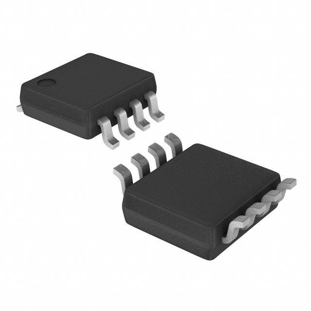
| 描述 | IC REDRIVER I2C 1CH 8VSSOP接口-信号缓冲器、中继器 Dual Bidirec I2C Bus and SMBus Repeater |
| 产品分类 | |
| 品牌 | Texas Instruments |
| 产品手册 | |
| 产品图片 |
|
| rohs | 符合RoHS无铅 / 符合限制有害物质指令(RoHS)规范要求 |
| 产品系列 | 接口 IC,接口-信号缓冲器、中继器,Texas Instruments PCA9515BDGKR- |
| 数据手册 | |
| 产品型号 | PCA9515BDGKR |
| PCN设计/规格 | |
| Tx/Rx型 | I2C Bus, SMBus |
| Tx/Rx类型 | I²C 逻辑 |
| 产品种类 | 接口-信号缓冲器、中继器 |
| 产品类型 | Repeaters |
| 传播延迟时间 | 45 ns |
| 供应商器件封装 | 8-VSSOP |
| 其它名称 | 296-30393-1 |
| 包装 | 剪切带 (CT) |
| 商标 | Texas Instruments |
| 安装类型 | 表面贴装 |
| 安装风格 | SMD/SMT |
| 封装 | Reel |
| 封装/外壳 | 8-TSSOP,8-MSOP(0.118",3.00mm 宽) |
| 封装/箱体 | VSSOP-8 |
| 工作温度 | -40°C ~ 85°C |
| 工作温度范围 | - 40 C to + 85 C |
| 工作电流 | 1 mA |
| 工作电源电压 | 2.3 V to 3.6 V |
| 工厂包装数量 | 2500 |
| 应用 | I²C |
| 延迟时间 | - |
| 数据速率(最大值) | 400kHz |
| 最大时钟频率 | 400 kHz |
| 标准包装 | 1 |
| 电压-电源 | 2.3 V ~ 3.6 V |
| 电容-输入 | 7pF |
| 电流-电源 | 500µA |
| 类型 | 缓冲器, 转接驱动器 |
| 系列 | PCA9515B |
| 输入 | 2 线式总线 |
| 输入电容 | 7 pF |
| 输出 | 2 线式总线 |
| 通道数 | 1 |
| 逻辑类型 | I2C Bus, SMBus |


- 商务部:美国ITC正式对集成电路等产品启动337调查
- 曝三星4nm工艺存在良率问题 高通将骁龙8 Gen1或转产台积电
- 太阳诱电将投资9.5亿元在常州建新厂生产MLCC 预计2023年完工
- 英特尔发布欧洲新工厂建设计划 深化IDM 2.0 战略
- 台积电先进制程称霸业界 有大客户加持明年业绩稳了
- 达到5530亿美元!SIA预计今年全球半导体销售额将创下新高
- 英特尔拟将自动驾驶子公司Mobileye上市 估值或超500亿美元
- 三星加码芯片和SET,合并消费电子和移动部门,撤换高东真等 CEO
- 三星电子宣布重大人事变动 还合并消费电子和移动部门
- 海关总署:前11个月进口集成电路产品价值2.52万亿元 增长14.8%


PDF Datasheet 数据手册内容提取
Product Sample & Technical Tools & Support & Folder Buy Documents Software Community PCA9515B SCPS232B–MARCH2012–REVISEDMARCH2016 2 PCA9515B Dual Bidirectional I C Bus and SMBus Repeater 1 Features 2 Applications • Two-ChannelBidirectionalBuffers • Servers 1 • I2CBusandSMBusCompatible • Routers(TelecomSwitchingEquipment) • SupportforI2CStandardMode(100-kHz)and • IndustrialEquipment FastMode(400-kHz) • ProductswithManyI2CSlavesandLongPCB • Active-HighRepeater-EnableInput Traces • Open-DrainI2CInputandOutput 3 Description • 5.5-VTolerantI2CInputandOutputandEnable The PCA9515B is a BiCMOS dual bidirectional buffer InputSupportMixed-ModeSignalOperation integrated circuit intended for I2C bus and SMBus • Lockup-FreeOperation applications. The device contains two identical • AccommodatesStandardMode,FastModeI2C bidirectional open-drain buffer circuits that enables Devices,andMultipleMasters I2C and similar bus systems to be extended (or add • SupportsArbitrationandClockStretchingAcross slaves) without degrading system performance. The dual bidirectional I2C buffer is operational at 2.3 V to Repeater 3.6VV . • Powered-OffHigh-ImpedanceI2CPins CC The PCA9515B buffers both the serial data (SDA) • Latch-UpPerformanceExceeds100-mAPer and serial clock (SCL) signals on the I2C bus, while JESD78,ClassI retaining all the operating modes and features of the • ESDProtectionExceedsJESD22 I2C system. The device allows two buses, of 400-pF – 2000-VHuman-BodyModel(A114-A) bus capacitance, to be connected in an I2C application. – 1000-VCharged-DeviceModel(C101) DeviceInformation(1) PARTNUMBER PACKAGE BODYSIZE(NOM) PCA9515B VSSOP(8) 3.00mm×3.00mm (1) For all available packages, see the orderable addendum at theendofthedatasheet. SimplifiedSchematic VCC VCC VCC VCC EN I2C or SMBus SCL0 SCL1 I2C Slave Master (e.g. PCA9515B Devices Processor) SDA0 SDA1 GND 1 An IMPORTANT NOTICE at the end of this data sheet addresses availability, warranty, changes, use in safety-critical applications, intellectualpropertymattersandotherimportantdisclaimers.PRODUCTIONDATA.
PCA9515B SCPS232B–MARCH2012–REVISEDMARCH2016 www.ti.com Table of Contents 1 Features.................................................................. 1 8.2 FunctionalBlockDiagram.........................................9 2 Applications........................................................... 1 8.3 FeatureDescription...................................................9 3 Description............................................................. 1 8.4 DeviceFunctionalModes........................................10 4 RevisionHistory..................................................... 2 9 ApplicationandImplementation........................ 11 9.1 ApplicationInformation............................................11 5 PinConfigurationandFunctions......................... 3 9.2 TypicalApplication .................................................11 6 Specifications......................................................... 4 10 PowerSupplyRecommendations..................... 12 6.1 AbsoluteMaximumRatings .....................................4 11 Layout................................................................... 13 6.2 ESDRatings ............................................................4 6.3 RecommendedOperatingConditions.......................4 11.1 LayoutGuidelines.................................................13 6.4 ThermalInformation .................................................4 11.2 LayoutExample....................................................13 6.5 ElectricalCharacteristics...........................................5 12 DeviceandDocumentationSupport................. 14 6.6 TimingRequirements................................................5 12.1 DocumentationSupport .......................................14 6.7 SwitchingCharacteristics..........................................5 12.2 CommunityResources..........................................14 6.8 TypicalCharacteristics..............................................6 12.3 Trademarks...........................................................14 7 ParameterMeasurementInformation..................7 12.4 ElectrostaticDischargeCaution............................14 12.5 Glossary................................................................14 8 DetailedDescription.............................................. 8 13 Mechanical,Packaging,andOrderable 8.1 Overview...................................................................8 Information........................................................... 14 4 Revision History NOTE:Pagenumbersforpreviousrevisionsmaydifferfrompagenumbersinthecurrentversion. ChangesfromRevisionA(May2013)toRevisionB Page • AddedDeviceInformationtable,ESDRatingstable,FeatureDescriptionsection,DeviceFunctionalModes, ApplicationandImplementationsection,PowerSupplyRecommendationssection,Layoutsection,Deviceand DocumentationSupportsection,andMechanical,Packaging,andOrderableInformationsection. .................................... 1 • Deletedtheorderinginformation.SeePOAattheendofthedatasheet............................................................................... 1 ChangesfromOriginal(March2012)toRevisionA Page • UpdatedtheV andV -V specifications........................................................................................................................ 5 OL OL ILC 2 SubmitDocumentationFeedback Copyright©2012–2016,TexasInstrumentsIncorporated ProductFolderLinks:PCA9515B
PCA9515B www.ti.com SCPS232B–MARCH2012–REVISEDMARCH2016 5 Pin Configuration and Functions DGKPackage 8-PinVSSOP TopView NC 1 8 VCC SCL0 2 7 SCL1 SDA0 3 6 SDA1 GND 4 5 EN NC-Nointernalconnection PinFunctions PIN I/O DESCRIPTION NO. NAME 1 NC — Nointernalconnection 2 SCL0 I/O Serialclockbus0 3 SDA0 I/O Serialdatabus0 4 GND — Supplyground 5 EN I Active-highrepeaterenableinput 6 SDA1 I/O Serialdatabus1 7 SCL1 I/O Serialclockbus1 8 V — Supplypower CC Copyright©2012–2016,TexasInstrumentsIncorporated SubmitDocumentationFeedback 3 ProductFolderLinks:PCA9515B
PCA9515B SCPS232B–MARCH2012–REVISEDMARCH2016 www.ti.com 6 Specifications 6.1 Absolute Maximum Ratings overoperatingfree-airtemperaturerange(unlessotherwisenoted) (1) MIN MAX UNIT V Supplyvoltage –0.5 7 V CC V Enableinputvoltage (2) –0.5 7 V I V I2Cbusvoltage(2) –0.5 7 V I/O I Inputclampcurrent V <0 –50 mA IK I I Outputclampcurrent V <0 –50 mA OK O I Continuousoutputcurrent ±50 mA O ContinuouscurrentthroughV orGND ±100 mA CC T Storagetemperature –65 150 °C stg (1) StressesbeyondthoselistedunderAbsoluteMaximumRatingsmaycausepermanentdamagetothedevice.Thesearestressratings only,whichdonotimplyfunctionaloperationofthedeviceattheseoranyotherconditionsbeyondthoseindicatedunderRecommended OperatingConditions.Exposuretoabsolute-maximum-ratedconditionsforextendedperiodsmayaffectdevicereliability. (2) Theinputnegative-voltageandoutputvoltageratingsmaybeexceedediftheinputandoutputcurrentratingsareobserved. 6.2 ESD Ratings VALUE UNIT Electrostatic Human-bodymodel(HBM),perANSI/ESDA/JEDECJS-001(1) ±2000 V V (ESD) discharge Charged-devicemodel(CDM),perJEDECspecificationJESD22-C101(2) ±1000 (1) JEDECdocumentJEP155statesthat500-VHBMallowssafemanufacturingwithastandardESDcontrolprocess. (2) JEDECdocumentJEP157statesthat250-VCDMallowssafemanufacturingwithastandardESDcontrolprocess. 6.3 Recommended Operating Conditions MIN MAX UNIT V Supplyvoltage 2.3 3.6 V CC SDAandSCLinputs 0.7×V 5.5 CC V High-levelinputvoltage V IH ENinput 2 5.5 SDAandSCLinputs –0.5 0.3×V V (1) Low-levelinputvoltage CC V IL ENinput –0.5 0.8 V (1) SDAandSCLlow-levelinputvoltagecontention –0.5 0.4 V ILc V =2.3V 6 CC I Low-leveloutputcurrent mA OL V =3V 6 CC T Operatingfree-airtemperature –40 85 °C A (1) V specificationisfortheENinputandthefirstlowlevelseenbytheSDAxandSCLxlines.V isforthesecondandsubsequentlow IL ILc levelsseenbytheSDAxandSCLxlines.V mustbeatleast70mVbelowV . ILc OL 6.4 Thermal Information PCA9515B THERMALMETRIC(1) DGK(VSSOP) UNIT 8PINS R Junction-to-ambientthermalresistance(2) 170.8 °C/W θJA R Junction-to-case(top)thermalresistance 62.9 °C/W θJC(top) R Junction-to-boardthermalresistance 91.6 °C/W θJB ψ Junction-to-topcharacterizationparameter 9.5 °C/W JT ψ Junction-to-boardcharacterizationparameter 90.2 °C/W JB (1) Formoreinformationabouttraditionalandnewthermalmetrics,seetheSemiconductorandICPackageThermalMetricsapplication report,SPRA953. (2) ThepackagethermalimpedanceiscalculatedinaccordancewithJESD51-7. 4 SubmitDocumentationFeedback Copyright©2012–2016,TexasInstrumentsIncorporated ProductFolderLinks:PCA9515B
PCA9515B www.ti.com SCPS232B–MARCH2012–REVISEDMARCH2016 6.5 Electrical Characteristics overrecommendedoperatingfree-airtemperaturerange(unlessotherwisenoted) PARAMETER TESTCONDITIONS V MIN TYP(1) MAX UNIT CC V Inputdiodeclampvoltage I =–18mA 2.3Vto3.6V –1.2 V IK I SDAx, V Low-leveloutputvoltage I =20μAor6mA 2.3Vto3.6V 0.47 0.52 0.6 V OL SCLx OL Low-levelinputvoltagebelow SDAx, V –V guaranteedbydesign 2.3Vto3.6V 120 mV OL ILc low-leveloutputvoltage SCLx Bothchannelshigh, 2.7V 0.5 3 SDAx=SCLx=VCC 3.6V 0.5 3 Bothchannelslow, 2.7V 1 4 SDA0=SCL0=GNDand I Quiescentsupplycurrent SDA1=SCL1=open;or mA CC SDA0=SCL0=openand 3.6V 1 4 SDA1=SCL1=GND Incontention, 2.7V 1 4 SDAx=SCLx=GND 3.6V 1 4 SDAx, VI=3.6V ±1 SCLx V =0.2V 3 I I Inputcurrent 2.3Vto3.6V μA I V =V ±1 I CC EN V =0.2V –10 –20 I SDAx, VI=3.6V 0.5 I Leakagecurrent EN=LorH 0V μA off SCLx V =GND 0.5 I Leakagecurrentduring SDAx, I V =3.6V EN=LorH 0Vto2.3V 1 μA I(ramp) powerup SCLx I EN 3.3V 7 9 Cin Inputcapacitance SDAx, VI=3VorGND pF EN=H 3.3V 7 9 SCLx (1) Alltypicalvaluesareatnominalsupplyvoltage(V =2.5Vor3.3V)andT =25°C. CC A 6.6 Timing Requirements overrecommendedoperatingfree-airtemperaturerange(unlessotherwisenoted)(seeFigure3) V MIN MAX UNIT CC 2.5V±0.2V 100 t Setuptime,EN↑beforeStartcondition ns su 3.3V±0.3V 100 2.5V±0.2V 130 t Holdtime,EN↓afterStopcondition ns h 3.3V±0.3V 100 6.7 Switching Characteristics overrecommendedoperatingfree-airtemperaturerange,C ≤100pF(unlessotherwisenoted) L PARAMETER FROM TO V MIN TYP(1) MAX UNIT (INPUT) (OUTPUT) CC 2.5V±0.2V 45 82 130 t PZL Propagationdelaytime(2) SDA0,SCL0or SDA1,SCL1or 3.3V±0.3V 45 68 120 ns SDA1,SCL1 SDA0,SCL0 2.5V±0.2V 33 113 190 t PLZ 3.3V±0.3V 33 102 180 2.5V±0.2V 57 t 80% 20% tHL Outputtransitiontime(2) 3.3V±0.3V 58 ns (SDAx,SCLx) 2.5V±0.2V 148 t 20% 80% tLH 3.3V±0.3V 147 (1) Alltypicalvaluesareatnominalsupplyvoltage(V =2.5Vor3.3V)andT =25°C. CC A (2) DifferentloadresistanceandcapacitancealtertheRCtimeconstant,therebychangingthepropagationdelayandtransitiontimes. Copyright©2012–2016,TexasInstrumentsIncorporated SubmitDocumentationFeedback 5 ProductFolderLinks:PCA9515B
PCA9515B SCPS232B–MARCH2012–REVISEDMARCH2016 www.ti.com 6.8 Typical Characteristics 0.54 0.55 TA = -40qC TA = 25qC e (V) 0.52 e (V) 0.525 TA = 85qC g g a a olt olt 0.5 V 0.5 V ut ut utp utp 0.475 O O mit 0.48 mit Li Li 0.45 er- er- Low 0.46 VCC = 2.3 V Low 0.425 VCC = 3.3 V VCC = 5 V 0.44 0.4 0 0.001 0.002 0.003 0.004 0.005 0.006 0.0002 0.001 00..000066 Lower-Limit Output Current (A) Lower-Limit Output Current (mA) D004 D003 Figure1.OutputLowVoltage(V )vs.OutputLowCurrent Figure2.OutputLowVoltage(V )vs.OutputLowCurrent OL OL (I )forSCL0atDifferentV (I )forSCL0atDifferentTemperaturesforV =5V OL CC OL CC 6 SubmitDocumentationFeedback Copyright©2012–2016,TexasInstrumentsIncorporated ProductFolderLinks:PCA9515B
PCA9515B www.ti.com SCPS232B–MARCH2012–REVISEDMARCH2016 7 Parameter Measurement Information VCC VCC PULSE VIN VOUT RL= 1.35 kΩ S1 DUT GENERATOR GND RT CL= 50 pF (see Note A) (see Note B) TEST S1 tPLZ/tPZL VCC TEST CIRCUIT FOR OPEN-DRAIN OUTPUT Input VCC 1.5V 1.5V 0V tPZL tPLZ Output VCC 80% 80% 1.5V 1.5V 20% 20% VOL ttHL ttLH VOLTAGEWAVEFORMS PROPAGATION DELAY AND OUTPUTTRANSITIONTIMES A. R terminationresistanceshouldbeequaltoZ ofpulsegenerators. T OUT B. C includesprobeandjigcapacitance. L C. All input pulses are supplied by generators having the following characteristics: PRR ≤ 10 MHz, Z = 50 Ω, O slewrate≥1V/ns. D. Theoutputsaremeasuredoneatatime,withonetransitionpermeasurement. Figure3. TestCircuitandVoltageWaveforms Copyright©2012–2016,TexasInstrumentsIncorporated SubmitDocumentationFeedback 7 ProductFolderLinks:PCA9515B
PCA9515B SCPS232B–MARCH2012–REVISEDMARCH2016 www.ti.com 8 Detailed Description 8.1 Overview The PCA9515B is a BiCMOS dual bidirectional buffer integrated circuit intended for I2C bus and SMBus applications. The device contains two identical bidirectional open-drain buffer circuits that enables I2C and similar bus systems to be extended without degrading system performance. This device enables I2C and similar bus systems to be extended (and add more slaves) without degradation of performance. The dual bidirectionalI2Cbufferisoperationalat2.3Vto3.6VV . CC The PCA9515B buffers both the serial data (SDA) and serial clock (SCL) signals on the I2C bus, while retaining all the operating modes and features of the I2C system. The device allows two buses, of 400-pF buscapacitance,tobeconnectedinanI2Capplication. The I2C bus capacitance limit of 400 pF restricts the number of slave devices and bus length. Using the PCA9515B, a system designer can capacitively isolate two halves of a bus, thus accommodating more I2C devicesandlongertracelengths. The PCA9515B has an active-high enable (EN) input with an internal pull-up. This allows users to select when the repeater is active and isolate malfunctioning slaves on power-up reset. States should never be changed during an I2C operation. Disabling during a bus operation will hang the bus and enabling part way through a bus cycle may confuse the I2C parts being enabled. The EN input should only change state when theglobalbusandtherepeaterportareinanidlestatetopreventsystemfailures. The PCA9515B can also be used to operate two buses, one at 5 V interface levels and the other at 3.3 V interface levels. The buses may also function at 400-kHz or 100-kHz operating frequency. If the two buses are operating at different frequencies, the 100-kHz bus must be isolated if the operation of the 400-kHz bus is required. If the master is running at 400-kHz, the maximum system operating frequency may be less than 400kHzbecauseofthedelaysaddedbytherepeater. The low level outputs for each internal buffer are approximately 0.5 V; however, the input voltage of each internal buffer must be 70 mV or more below the low level output when the output is driven low internally. Thispreventsalockupconditionfromoccurringwhentheinputlowconditionisreleased. Two or more PCA9515B devices cannot be used in series. Since there is no direction pin, different valid low- voltage levels are used to avoid lockup conditions between the input and the output of each repeater. A valid low, applied at the input of a PCA9515B, is propagated as a buffered low with a higher value on the enabled outputs. When this buffered low is applied to another PCA9515B-type device in series, the second device doesnotrecognizeitasavalidlowanddoesnotpropagateitasabufferedlow. The device contains a power-up control circuit that sets an internal latch to prevent the output circuits from becomingactiveuntilV isatavalidlevel(V =2.3V). CC CC As with the standard I2C system, pullup resistors are required to provide the logic high levels on the buffered bus.ThePCA9515Bhasstandardopen-collectorconfigurationoftheI2Cbus.Thesizeofthepullupresistors depend on the system; however, each side of the repeater must have a pullup resistor. The device is designed to work with Standard Mode and Fast Mode I2C devices in addition to SMBus devices. Standard Mode I2C devices only specify a 3 mA termination current in a generic I2C system where Standard Mode devices and multiple masters are possible. Under certain conditions, high termination currentscanbeused. 8 SubmitDocumentationFeedback Copyright©2012–2016,TexasInstrumentsIncorporated ProductFolderLinks:PCA9515B
PCA9515B www.ti.com SCPS232B–MARCH2012–REVISEDMARCH2016 8.2 Functional Block Diagram VCC 8 PCA9515B 3 6 SDA0 SDA1 2 7 SCL0 SCL1 Pullup Resistor 5 EN 4 Figure4. LogicDiagram(PoisitveLogic) 8.3 Feature Description 8.3.1 Two-ChannelBidirectionalBuffer ThePCA9515Bisatwo-channelbidirectionalbufferforopen-drainapplicationslikeI2CandSMBus. 8.3.2 BidirectionalVoltage-LevelTranslation The PCA9515B allows bidirectional voltage-level translation (up-translation and down-translation) between low voltages(downto2.3V)andhighervoltages(upto5.5V). 8.3.3 Active-HighEnableInput The PCA9515B has an active-high enable (EN) input with an internal pull-up to V . The enable input needs to CC be pulled to GND to disable the PCA9515B and isolate the I2C buses. Pulling-up the enable pin or floating the enablepincausesthePCA9515BtoturnonandbuffertheI2Cbus. Copyright©2012–2016,TexasInstrumentsIncorporated SubmitDocumentationFeedback 9 ProductFolderLinks:PCA9515B
PCA9515B SCPS232B–MARCH2012–REVISEDMARCH2016 www.ti.com 8.4 Device Functional Modes The PCA9515B has an active-high enable (EN) input with an internal pull-up to V , which allows the user to CC select when the repeater is active. This can be used to isolate a badly behaved slave on power-up reset. It should never change state during an I2C operation, because disabling during a bus operation my hang the bus, and enabling part way through the bus cycles could confuse the I2C parts being enabled. The EN input should only change state when the global bus and repeater port are in the idle state to prevent system failures. Table 1 liststhePCA9515Bfunctions. Table1.FunctionTable INPUT FUNCTION EN L Outputsdisabled SDA0=SDA1, H SCL0=SCL1 10 SubmitDocumentationFeedback Copyright©2012–2016,TexasInstrumentsIncorporated ProductFolderLinks:PCA9515B
PCA9515B www.ti.com SCPS232B–MARCH2012–REVISEDMARCH2016 9 Application and Implementation NOTE Information in the following applications sections is not part of the TI component specification, and TI does not warrant its accuracy or completeness. TI’s customers are responsible for determining suitability of components for their purposes. Customers should validateandtesttheirdesignimplementationtoconfirmsystemfunctionality. 9.1 Application Information The PCA9515B is typically used to buffer an I2C signal, isolating capacitance from two sides of the bus. This allows for longer traces and cables, and a more robust I2C communication. Typical Application section describes how the PCA9515B may be used to isolate a standard mode and fast mode I2C bus, to allow for faster communicationswhenrequired,butmaintainingcompatibilitywiththeslowerstandardmodeslavedevice. It is critical to keep the V and V requirements in mind when designing with buffers, especially when using OL IL multiple buffers/translators on the same node. Care must be taken to not violate the V requirement of a buffer, IL otherwise I2C communication errors will occur. An example of this would be a buffer with a V of ~0.5 V, and a OL device requires a V of less than 0.4 V. Such a connection would result in the slave device being unable to IL recognizetheoutputlowsignalasavalidlow. 9.2 Typical Application AtypicalapplicationisshowninFigure5.Inthisexample,thesystemmasterisrunningona3.3VI2Cbus,while the slave is connected to a 5-V bus. Both buses run at 100 kHz, unless the slave bus is isolated. If the slave bus is isolated (by pulling the EN pin low), the master bus can run at 400 kHz. Master devices can be placed on eitherbus,thePCA9515Bdoesnotcarewhichsidethemasterison.Decouplingcapacitorsarerequired,butare notshowninFigure5forsimplicity. 3.3 V 5 V SDA SDA0 SDA1 SDA SCL SCL0 SCL1 SCL PCA9515B I2C BUS MASTER I2C BUS SLAVE 400 kHz EN 100 kHz BUS 0 BUS 1 Figure5. TypicalApplication 9.2.1 DesignRequirements Table2liststhedesignrequirements. Table2.DesignRequirements PARAMETER VALUE Input-sideI2Csignal 3.3V Output-sideI2Csignal 5V Copyright©2012–2016,TexasInstrumentsIncorporated SubmitDocumentationFeedback 11 ProductFolderLinks:PCA9515B
PCA9515B SCPS232B–MARCH2012–REVISEDMARCH2016 www.ti.com 9.2.2 DetailedDesignProcedure The PCA9515B is 5.5 V tolerant, so it does not require any additional circuitry to translate between the different busvoltages.WhenonesideofthePCA9515BispulledlowbyadeviceontheI2Cbus,aCMOShysteresis-type input detects the falling edge and causes an internal driver on the other side to turn on, thus causing the other sidealsotogolow.ThesidedrivenlowbythePCA9515BtypicallyisatV =0.5V. OL Figure 6 and Figure 7 show the waveforms that are seen in a typical application. If the bus master in Figure 5 writes to the slave through the PCA9515B, Bus 0 has the waveform shown in Figure 6. The waveform looks like a normal I2C transmission until the falling edge of the eighth clock pulse. At that point, the master releases the dataline(SDA)whiletheslavepullsitlowthroughthePCA9515B.BecausetheV ofthePCA9515Btypicallyis OL around 0.5 V, a step in the SDA is seen. After the master has transmitted the ninth clock pulse, the slave releasesthedataline. On the Bus 1 side of the PCA9515B, the clock and data lines have a positive offset from ground equal to the V OL ofthePCA9515B.Aftertheeighthclockpulse,thedatalineispulledtotheV oftheslavedevice,whichisvery OL closetogroundintheexample. 9.2.3 ApplicationCurves 9th Clock Pulse SCL SDA V of Master V of PCA9515B OL OL Figure6. Bus0Waveforms 9th Clock Pulse SCL SDA VOLof PCA9515B VOLof Slave Figure7. Bus1Waveforms 10 Power Supply Recommendations For V , a 2.3 V to 3.6 V power supply is required. Standard decoupling capacitors are recommended. These CC capacitors typically range from 0.1 µF to 1 µF, but the ideal capacitance depends on the amount of noise from thepowersupply. 12 SubmitDocumentationFeedback Copyright©2012–2016,TexasInstrumentsIncorporated ProductFolderLinks:PCA9515B
PCA9515B www.ti.com SCPS232B–MARCH2012–REVISEDMARCH2016 11 Layout 11.1 Layout Guidelines For printed circuit board (PCB) layout of the PCA9515B, common PCB layout practices should be followed. In all PCB layouts, it is a best practice to avoid right angles in signal traces, to fan out signal traces away from each other upon leaving the vicinity of an integrated circuit (IC), and to use thicker trace widths to carry higher amounts of current that commonly pass through power and ground traces. By-pass and de-coupling capacitors are commonly used to control the voltage on the V pin, using a larger capacitor to provide additional power in CC the event of a short power supply glitch and a small capacitor to filter out high-frequency ripple. These decouplingcapacitorsshouldbeplacedasclosetotheV pinofPCA9515Baspossible. CC The layout example shown in Figure 8 shows a 4 layer board, which is preferable for boards with higher density signalrouting.Ona4layerPCB,itiscommontoroutesignalsonthetopandbottomlayer,dedicateoneinternal layer to a ground plane, and one to power plane. In a board layout using planes or split planes for power and ground, vias are placed directly next to the surface mount component pad which needs to attach to V or GND CC and the via is connected electrically to the internal layer on the other side of the board. Vias are also used when a signal trace needs to be routed to the opposite side of the board. This routing and via is not necessary if V CC andGNDarebothfullplanesasopposedtothepartialplanesdepicted. 11.2 Layout Example Via to V Plane CC Via to GND Plane Via to Bottom layer Decoupling Capacitor V C C G N NC 1 8 VCC D SCL02 7SCL1 PCA9515B SDA03 6SDA1 GND 4 5 EN Figure8. LayoutSchematic Copyright©2012–2016,TexasInstrumentsIncorporated SubmitDocumentationFeedback 13 ProductFolderLinks:PCA9515B
PCA9515B SCPS232B–MARCH2012–REVISEDMARCH2016 www.ti.com 12 Device and Documentation Support 12.1 Documentation Support 12.1.1 RelatedDocumentation Forrelateddocumentationseethefollowing: • I2CBusPullupResistorCalculation,SLVA689 • MaximumClockFrequencyofI2CBusUsingRepeaters,SLVA695 • IntroductiontoLogic,SLVA700 • UnderstandingtheI2CBus,SLVA704 12.2 Community Resources The following links connect to TI community resources. Linked contents are provided "AS IS" by the respective contributors. They do not constitute TI specifications and do not necessarily reflect TI's views; see TI's Terms of Use. TIE2E™OnlineCommunity TI'sEngineer-to-Engineer(E2E)Community.Createdtofostercollaboration amongengineers.Ate2e.ti.com,youcanaskquestions,shareknowledge,exploreideasandhelp solveproblemswithfellowengineers. DesignSupport TI'sDesignSupport QuicklyfindhelpfulE2Eforumsalongwithdesignsupporttoolsand contactinformationfortechnicalsupport. 12.3 Trademarks E2EisatrademarkofTexasInstruments. Allothertrademarksarethepropertyoftheirrespectiveowners. 12.4 Electrostatic Discharge Caution This integrated circuit can be damaged by ESD. Texas Instruments recommends that all integrated circuits be handled with appropriateprecautions.Failuretoobserveproperhandlingandinstallationprocedurescancausedamage. ESDdamagecanrangefromsubtleperformancedegradationtocompletedevicefailure.Precisionintegratedcircuitsmaybemore susceptibletodamagebecauseverysmallparametricchangescouldcausethedevicenottomeetitspublishedspecifications. 12.5 Glossary SLYZ022—TIGlossary. Thisglossarylistsandexplainsterms,acronyms,anddefinitions. 13 Mechanical, Packaging, and Orderable Information The following pages include mechanical, packaging, and orderable information. This information is the most current data available for the designated devices. This data is subject to change without notice and revision of thisdocument.Forbrowser-basedversionsofthisdatasheet,refertotheleft-handnavigation. 14 SubmitDocumentationFeedback Copyright©2012–2016,TexasInstrumentsIncorporated ProductFolderLinks:PCA9515B
PACKAGE OPTION ADDENDUM www.ti.com 6-Feb-2020 PACKAGING INFORMATION Orderable Device Status Package Type Package Pins Package Eco Plan Lead/Ball Finish MSL Peak Temp Op Temp (°C) Device Marking Samples (1) Drawing Qty (2) (6) (3) (4/5) PCA9515BDGKR ACTIVE VSSOP DGK 8 2500 Green (RoHS NIPDAU | NIPDAUAG Level-1-260C-UNLIM -40 to 85 (7SE, 7SF) & no Sb/Br) (1) The marketing status values are defined as follows: ACTIVE: Product device recommended for new designs. LIFEBUY: TI has announced that the device will be discontinued, and a lifetime-buy period is in effect. NRND: Not recommended for new designs. Device is in production to support existing customers, but TI does not recommend using this part in a new design. PREVIEW: Device has been announced but is not in production. Samples may or may not be available. OBSOLETE: TI has discontinued the production of the device. (2) RoHS: TI defines "RoHS" to mean semiconductor products that are compliant with the current EU RoHS requirements for all 10 RoHS substances, including the requirement that RoHS substance do not exceed 0.1% by weight in homogeneous materials. Where designed to be soldered at high temperatures, "RoHS" products are suitable for use in specified lead-free processes. TI may reference these types of products as "Pb-Free". RoHS Exempt: TI defines "RoHS Exempt" to mean products that contain lead but are compliant with EU RoHS pursuant to a specific EU RoHS exemption. Green: TI defines "Green" to mean the content of Chlorine (Cl) and Bromine (Br) based flame retardants meet JS709B low halogen requirements of <=1000ppm threshold. Antimony trioxide based flame retardants must also meet the <=1000ppm threshold requirement. (3) MSL, Peak Temp. - The Moisture Sensitivity Level rating according to the JEDEC industry standard classifications, and peak solder temperature. (4) There may be additional marking, which relates to the logo, the lot trace code information, or the environmental category on the device. (5) Multiple Device Markings will be inside parentheses. Only one Device Marking contained in parentheses and separated by a "~" will appear on a device. If a line is indented then it is a continuation of the previous line and the two combined represent the entire Device Marking for that device. (6) Lead/Ball Finish - Orderable Devices may have multiple material finish options. Finish options are separated by a vertical ruled line. Lead/Ball Finish values may wrap to two lines if the finish value exceeds the maximum column width. Important Information and Disclaimer:The information provided on this page represents TI's knowledge and belief as of the date that it is provided. TI bases its knowledge and belief on information provided by third parties, and makes no representation or warranty as to the accuracy of such information. Efforts are underway to better integrate information from third parties. TI has taken and continues to take reasonable steps to provide representative and accurate information but may not have conducted destructive testing or chemical analysis on incoming materials and chemicals. TI and TI suppliers consider certain information to be proprietary, and thus CAS numbers and other limited information may not be available for release. In no event shall TI's liability arising out of such information exceed the total purchase price of the TI part(s) at issue in this document sold by TI to Customer on an annual basis. Addendum-Page 1
PACKAGE MATERIALS INFORMATION www.ti.com 10-May-2019 TAPE AND REEL INFORMATION *Alldimensionsarenominal Device Package Package Pins SPQ Reel Reel A0 B0 K0 P1 W Pin1 Type Drawing Diameter Width (mm) (mm) (mm) (mm) (mm) Quadrant (mm) W1(mm) PCA9515BDGKR VSSOP DGK 8 2500 330.0 12.4 5.3 3.4 1.4 8.0 12.0 Q1 PCA9515BDGKR VSSOP DGK 8 2500 330.0 12.4 5.3 3.3 1.3 8.0 12.0 Q1 PackMaterials-Page1
PACKAGE MATERIALS INFORMATION www.ti.com 10-May-2019 *Alldimensionsarenominal Device PackageType PackageDrawing Pins SPQ Length(mm) Width(mm) Height(mm) PCA9515BDGKR VSSOP DGK 8 2500 364.0 364.0 27.0 PCA9515BDGKR VSSOP DGK 8 2500 346.0 346.0 35.0 PackMaterials-Page2
None
None
IMPORTANTNOTICEANDDISCLAIMER TI PROVIDES TECHNICAL AND RELIABILITY DATA (INCLUDING DATASHEETS), DESIGN RESOURCES (INCLUDING REFERENCE DESIGNS), APPLICATION OR OTHER DESIGN ADVICE, WEB TOOLS, SAFETY INFORMATION, AND OTHER RESOURCES “AS IS” AND WITH ALL FAULTS, AND DISCLAIMS ALL WARRANTIES, EXPRESS AND IMPLIED, INCLUDING WITHOUT LIMITATION ANY IMPLIED WARRANTIES OF MERCHANTABILITY, FITNESS FOR A PARTICULAR PURPOSE OR NON-INFRINGEMENT OF THIRD PARTY INTELLECTUAL PROPERTY RIGHTS. These resources are intended for skilled developers designing with TI products. You are solely responsible for (1) selecting the appropriate TI products for your application, (2) designing, validating and testing your application, and (3) ensuring your application meets applicable standards, and any other safety, security, or other requirements. These resources are subject to change without notice. TI grants you permission to use these resources only for development of an application that uses the TI products described in the resource. Other reproduction and display of these resources is prohibited. No license is granted to any other TI intellectual property right or to any third party intellectual property right. TI disclaims responsibility for, and you will fully indemnify TI and its representatives against, any claims, damages, costs, losses, and liabilities arising out of your use of these resources. TI’s products are provided subject to TI’s Terms of Sale (www.ti.com/legal/termsofsale.html) or other applicable terms available either on ti.com or provided in conjunction with such TI products. TI’s provision of these resources does not expand or otherwise alter TI’s applicable warranties or warranty disclaimers for TI products. Mailing Address: Texas Instruments, Post Office Box 655303, Dallas, Texas 75265 Copyright © 2020, Texas Instruments Incorporated