ICGOO在线商城 > 集成电路(IC) > PMIC - 显示器驱动器 > PCA85176H/Q900/1,5

 Datasheet下载
- 型号: PCA85176H/Q900/1,5
- 制造商: NXP Semiconductors
- 库位|库存: xxxx|xxxx
- 要求:
| 数量阶梯 | 香港交货 | 国内含税 |
| +xxxx | $xxxx | ¥xxxx |
查看当月历史价格
查看今年历史价格
PCA85176H/Q900/1,5产品简介:
ICGOO电子元器件商城为您提供PCA85176H/Q900/1,5由NXP Semiconductors设计生产,在icgoo商城现货销售,并且可以通过原厂、代理商等渠道进行代购。 PCA85176H/Q900/1,5价格参考。NXP SemiconductorsPCA85176H/Q900/1,5封装/规格:PMIC - 显示器驱动器, 。您可以下载PCA85176H/Q900/1,5参考资料、Datasheet数据手册功能说明书,资料中有PCA85176H/Q900/1,5 详细功能的应用电路图电压和使用方法及教程。
NXP PCA85176H/Q900/1.5 是一款 PMIC(电源管理集成电路),专为显示器驱动应用设计。以下是其主要应用场景:

 1. 汽车显示系统
   - 该芯片广泛应用于汽车仪表盘、中控显示屏、抬头显示(HUD)以及后视镜显示屏等场景。
   - 提供高效的电源管理,支持高分辨率和低功耗的显示需求。
   - 具备良好的电磁兼容性(EMC),满足汽车环境中的严格标准。

 2. 工业显示器
   - 适用于工业控制面板、人机界面(HMI)、医疗设备显示屏等。
   - 提供稳定可靠的电源输出,确保在复杂工业环境中正常运行。
   - 支持宽工作温度范围,适应恶劣环境条件。

 3. 消费电子
   - 可用于智能电视、平板电脑、笔记本电脑等消费类电子产品的显示模块。
   - 集成多种电源轨管理功能,优化系统功耗并延长电池寿命。

 4. 可穿戴设备
   - 支持小型化、低功耗的显示驱动需求,适用于智能手表、健身追踪器等可穿戴设备。
   - 提供高效的电源转换效率,减少发热并提升续航能力。

 5. 嵌入式系统
   - 在嵌入式系统中,用于驱动 OLED、LCD 或其他类型的显示屏。
   - 提供灵活的配置选项,满足不同尺寸和分辨率的显示需求。

 核心优势:
- 高效电源管理:集成多路电压调节器,降低功耗。
- 高可靠性:符合 AEC-Q100 标准,适合汽车级应用。
- 小尺寸封装:节省 PCB 空间,便于紧凑型设计。
- 多功能集成:简化系统设计,减少外部组件数量。

综上所述,PCA85176H/Q900/1.5 主要应用于需要高性能、低功耗和高可靠性的显示驱动场景,特别是在汽车、工业和消费电子领域具有广泛用途。
| 参数 | 数值 |
| 产品目录 | 集成电路 (IC) |
| 描述 | IC LCD DRIVER 40SEG 64TQFP |
| 产品分类 | |
| 品牌 | NXP Semiconductors |
| 数据手册 | |
| 产品图片 |
|
| 产品型号 | PCA85176H/Q900/1,5 |
| PCN设计/规格 | |
| rohs | 无铅 / 符合限制有害物质指令(RoHS)规范要求 |
| 产品系列 | - |
| 产品培训模块 | http://www.digikey.cn/PTM/IndividualPTM.page?site=cn&lang=zhs&ptm=25410 |
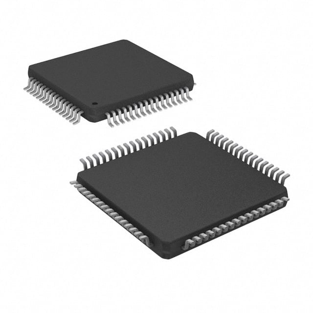
| 供应商器件封装 | 64-TQFP(10x10) |
| 其它名称 | 568-5108-6 |
| 包装 | Digi-Reel® |
| 安装类型 | 表面贴装 |
| 封装/外壳 | 64-TQFP |
| 工作温度 | -40°C ~ 95°C |
| 接口 | I²C |
| 数字或字符 | - |
| 显示类型 | LCD |
| 标准包装 | 1 |
| 电压-电源 | 1.8 V ~ 5.5 V |
| 电流-电源 | 3.5µA |
| 配置 | 40 段 |


- 商务部:美国ITC正式对集成电路等产品启动337调查
- 曝三星4nm工艺存在良率问题 高通将骁龙8 Gen1或转产台积电
- 太阳诱电将投资9.5亿元在常州建新厂生产MLCC 预计2023年完工
- 英特尔发布欧洲新工厂建设计划 深化IDM 2.0 战略
- 台积电先进制程称霸业界 有大客户加持明年业绩稳了
- 达到5530亿美元!SIA预计今年全球半导体销售额将创下新高
- 英特尔拟将自动驾驶子公司Mobileye上市 估值或超500亿美元
- 三星加码芯片和SET,合并消费电子和移动部门,撤换高东真等 CEO
- 三星电子宣布重大人事变动 还合并消费电子和移动部门
- 海关总署:前11个月进口集成电路产品价值2.52万亿元 增长14.8%


PDF Datasheet 数据手册内容提取
PCA85176 40 x 4 automotive LCD driver for low multiplex rates Rev. 6 — 7 April 2015 Product data sheet 1. General description The PCA85176 is a peripheral device which interfaces to almost any Liquid Crystal Display(LCD)1 with low multiplex rates. It generates the drive signals for any static or multiplexed LCD containing up to four backplanes and up to 40segments. It can be easily cascaded for larger LCD applications. The PCA85176 is compatible with most microcontrollers and communicates via the two-line bidirectional I2C-bus. Communication overheads are minimized by a display RAM with auto-incremented addressing, by hardware subaddressing, and by display memory switching (static and duplex drive modes). For a selection of NXP LCD segment drivers, see Table24 on page51. 2. Features and benefits AEC-Q100 compliant for automotive applications Single chip LCD controller and driver Selectable backplane drive configuration: static, 2, 3, or 4 backplane multiplexing Selectable display bias configuration: static, 1⁄ , or 1⁄ 2 3 Internal LCD bias generation with voltage-follower buffers 40segment drives: Up to 20 7-segment numeric characters Up to 10 14-segment alphanumeric characters Any graphics of up to 160segments/elements 40 4-bit RAM for display data storage Auto-incremented display data loading across device subaddress boundaries Display memory bank switching in static and duplex drive modes Versatile blinking modes Independent supplies possible for LCD and logic voltages Wide power supply range: from 1.8V to 5.5V Wide logic LCD supply range: From 2.5V for low-threshold LCDs Up to 8.0V for guest-host LCDs and high-threshold twisted nematic LCDs Low power consumption Extended temperature range up to 95 C 400kHz I2C-bus interface May be cascaded for large LCD applications (up to 2560segments/elements possible) No external components required 1. The definition of the abbreviations and acronyms used in this data sheet can be found in Section22.
PCA85176 NXP Semiconductors 40 x 4 automotive LCD driver for low multiplex rates Manufactured in silicon gate CMOS process 3. Ordering information Table 1. Ordering information Type number Package Name Description Version PCA85176H TQFP64 plastic thin quad flat package, 64leads; SOT357-1 body10101.0mm PCA85176T TSSOP56 plastic thin shrink small outline package, SOT364-1 56 leads; bodywidth6.1 mm 3.1 Ordering options Table 2. Ordering opt ions Type number Orderable part number Sales item (12NC) Delivery form IC revision PCA85176H/Q900/1 PCA85176H/Q900/1,5 935290065518 tape and reel, 13 inch, dry pack 1 PCA85176T/Q900/1 PCA85176T/Q900/1,1 935290076118 tape and reel, 13 inch 1 4. Marking Table 3. Marking codes Type number Marking code PCA85176H/Q900/1 PCA85176H PCA85176T/Q900/1 PCA85176T PCA85176 All information provided in this document is subject to legal disclaimers. © NXP Semiconductors N.V. 2015. All rights reserved. Product data sheet Rev. 6 — 7 April 2015 2 of 60
PCA85176 NXP Semiconductors 40 x 4 automotive LCD driver for low multiplex rates 5. Block diagram (cid:37)(cid:51)(cid:19) (cid:37)(cid:51)(cid:21) (cid:37)(cid:51)(cid:20) (cid:37)(cid:51)(cid:22) (cid:54)(cid:19)(cid:3)(cid:87)(cid:82)(cid:3)(cid:54)(cid:22)(cid:28) (cid:23)(cid:19) (cid:57)(cid:47)(cid:38)(cid:39) (cid:37)(cid:36)(cid:38)(cid:46)(cid:51)(cid:47)(cid:36)(cid:49)(cid:40) (cid:39)(cid:44)(cid:54)(cid:51)(cid:47)(cid:36)(cid:60)(cid:3)(cid:54)(cid:40)(cid:42)(cid:48)(cid:40)(cid:49)(cid:55) (cid:50)(cid:56)(cid:55)(cid:51)(cid:56)(cid:55)(cid:54) (cid:50)(cid:56)(cid:55)(cid:51)(cid:56)(cid:55)(cid:54) (cid:47)(cid:38)(cid:39) (cid:39)(cid:44)(cid:54)(cid:51)(cid:47)(cid:36)(cid:60) (cid:57)(cid:50)(cid:47)(cid:55)(cid:36)(cid:42)(cid:40) (cid:53)(cid:40)(cid:42)(cid:44)(cid:54)(cid:55)(cid:40)(cid:53) (cid:54)(cid:40)(cid:47)(cid:40)(cid:38)(cid:55)(cid:50)(cid:53) (cid:47)(cid:38)(cid:39)(cid:3)(cid:37)(cid:44)(cid:36)(cid:54) (cid:39)(cid:44)(cid:54)(cid:51)(cid:47)(cid:36)(cid:60) (cid:50)(cid:56)(cid:55)(cid:51)(cid:56)(cid:55)(cid:3)(cid:37)(cid:36)(cid:49)(cid:46)(cid:3)(cid:54)(cid:40)(cid:47)(cid:40)(cid:38)(cid:55) (cid:42)(cid:40)(cid:49)(cid:40)(cid:53)(cid:36)(cid:55)(cid:50)(cid:53) (cid:38)(cid:50)(cid:49)(cid:55)(cid:53)(cid:50)(cid:47)(cid:47)(cid:40)(cid:53) (cid:36)(cid:49)(cid:39)(cid:3)(cid:37)(cid:47)(cid:44)(cid:49)(cid:46)(cid:3)(cid:38)(cid:50)(cid:49)(cid:55)(cid:53)(cid:50)(cid:47) (cid:57)(cid:54)(cid:54) (cid:38)(cid:47)(cid:46) (cid:38)(cid:47)(cid:50)(cid:38)(cid:46)(cid:3)(cid:54)(cid:40)(cid:47)(cid:40)(cid:38)(cid:55) (cid:37)(cid:47)(cid:44)(cid:49)(cid:46)(cid:40)(cid:53) (cid:51)(cid:38)(cid:36)(cid:27)(cid:24)(cid:20)(cid:26)(cid:25) (cid:39)(cid:44)(cid:54)(cid:51)(cid:47)(cid:36)(cid:60)(cid:3)(cid:53)(cid:36)(cid:48) (cid:36)(cid:49)(cid:39)(cid:3)(cid:55)(cid:44)(cid:48)(cid:44)(cid:49)(cid:42) (cid:55)(cid:44)(cid:48)(cid:40)(cid:37)(cid:36)(cid:54)(cid:40) (cid:54)(cid:60)(cid:49)(cid:38) (cid:51)(cid:50)(cid:58)(cid:40)(cid:53)(cid:16)(cid:50)(cid:49) (cid:38)(cid:50)(cid:48)(cid:48)(cid:36)(cid:49)(cid:39) (cid:58)(cid:53)(cid:44)(cid:55)(cid:40)(cid:3)(cid:39)(cid:36)(cid:55)(cid:36) (cid:39)(cid:36)(cid:55)(cid:36)(cid:3)(cid:51)(cid:50)(cid:44)(cid:49)(cid:55)(cid:40)(cid:53)(cid:3)(cid:36)(cid:49)(cid:39) (cid:50)(cid:54)(cid:38) (cid:50)(cid:54)(cid:38)(cid:44)(cid:47)(cid:47)(cid:36)(cid:55)(cid:50)(cid:53) (cid:53)(cid:40)(cid:54)(cid:40)(cid:55) (cid:39)(cid:40)(cid:38)(cid:50)(cid:39)(cid:40)(cid:53) (cid:38)(cid:50)(cid:49)(cid:55)(cid:53)(cid:50)(cid:47) (cid:36)(cid:56)(cid:55)(cid:50)(cid:3)(cid:44)(cid:49)(cid:38)(cid:53)(cid:40)(cid:48)(cid:40)(cid:49)(cid:55) (cid:57)(cid:39)(cid:39) (cid:54)(cid:38)(cid:47) (cid:44)(cid:49)(cid:51)(cid:56)(cid:55) (cid:44)(cid:21)(cid:38)(cid:16)(cid:37)(cid:56)(cid:54) (cid:54)(cid:56)(cid:37)(cid:36)(cid:39)(cid:39)(cid:53)(cid:40)(cid:54)(cid:54) (cid:41)(cid:44)(cid:47)(cid:55)(cid:40)(cid:53)(cid:54) (cid:38)(cid:50)(cid:49)(cid:55)(cid:53)(cid:50)(cid:47)(cid:47)(cid:40)(cid:53) (cid:38)(cid:50)(cid:56)(cid:49)(cid:55)(cid:40)(cid:53) (cid:54)(cid:39)(cid:36) (cid:54)(cid:36)(cid:19) (cid:36)(cid:19) (cid:36)(cid:20) (cid:36)(cid:21) (cid:19)(cid:20)(cid:22)(cid:68)(cid:68)(cid:68)(cid:19)(cid:23)(cid:27) Fig 1. Block diagram of PCA85176 PCA85176 All information provided in this document is subject to legal disclaimers. © NXP Semiconductors N.V. 2015. All rights reserved. Product data sheet Rev. 6 — 7 April 2015 3 of 60
PCA85176 NXP Semiconductors 40 x 4 automotive LCD driver for low multiplex rates 6. Pinning information 6.1 Pinning (cid:22) (cid:21) (cid:20) (cid:19) (cid:28) (cid:27) (cid:26) (cid:25) (cid:24) (cid:23) (cid:22) (cid:21) (cid:20) (cid:19) (cid:28) (cid:27) (cid:22) (cid:22) (cid:22) (cid:22) (cid:21) (cid:21) (cid:21) (cid:21) (cid:21) (cid:21) (cid:21) (cid:21) (cid:21) (cid:21) (cid:20) (cid:20) (cid:54) (cid:54) (cid:54) (cid:54) (cid:54) (cid:54) (cid:54) (cid:54) (cid:54) (cid:54) (cid:54) (cid:54) (cid:54) (cid:54) (cid:54) (cid:54) (cid:23) (cid:22) (cid:21) (cid:20) (cid:19) (cid:28) (cid:27) (cid:26) (cid:25) (cid:24) (cid:23) (cid:22) (cid:21) (cid:20) (cid:19) (cid:28) (cid:25) (cid:25) (cid:25) (cid:25) (cid:25) (cid:24) (cid:24) (cid:24) (cid:24) (cid:24) (cid:24) (cid:24) (cid:24) (cid:24) (cid:24) (cid:23) (cid:81)(cid:17)(cid:70)(cid:17) (cid:20) (cid:23)(cid:27) (cid:81)(cid:17)(cid:70)(cid:17) (cid:54)(cid:22)(cid:23) (cid:21) (cid:23)(cid:26) (cid:54)(cid:20)(cid:26) (cid:54)(cid:22)(cid:24) (cid:22) (cid:23)(cid:25) (cid:54)(cid:20)(cid:25) (cid:54)(cid:22)(cid:25) (cid:23) (cid:23)(cid:24) (cid:54)(cid:20)(cid:24) (cid:54)(cid:22)(cid:26) (cid:24) (cid:23)(cid:23) (cid:54)(cid:20)(cid:23) (cid:54)(cid:22)(cid:27) (cid:25) (cid:23)(cid:22) (cid:54)(cid:20)(cid:22) (cid:54)(cid:22)(cid:28) (cid:26) (cid:23)(cid:21) (cid:54)(cid:20)(cid:21) (cid:81)(cid:17)(cid:70)(cid:17) (cid:27) (cid:23)(cid:20) (cid:54)(cid:20)(cid:20) (cid:51)(cid:38)(cid:36)(cid:27)(cid:24)(cid:20)(cid:26)(cid:25)(cid:43) (cid:81)(cid:17)(cid:70)(cid:17) (cid:28) (cid:23)(cid:19) (cid:54)(cid:20)(cid:19) (cid:54)(cid:39)(cid:36) (cid:20)(cid:19) (cid:22)(cid:28) (cid:54)(cid:28) (cid:54)(cid:38)(cid:47) (cid:20)(cid:20) (cid:22)(cid:27) (cid:54)(cid:27) (cid:54)(cid:60)(cid:49)(cid:38) (cid:20)(cid:21) (cid:22)(cid:26) (cid:54)(cid:26) (cid:38)(cid:47)(cid:46) (cid:20)(cid:22) (cid:22)(cid:25) (cid:54)(cid:25) (cid:57)(cid:39)(cid:39) (cid:20)(cid:23) (cid:22)(cid:24) (cid:54)(cid:24) (cid:50)(cid:54)(cid:38) (cid:20)(cid:24) (cid:22)(cid:23) (cid:54)(cid:23) (cid:36)(cid:19) (cid:20)(cid:25) (cid:22)(cid:22) (cid:81)(cid:17)(cid:70)(cid:17) (cid:26) (cid:27) (cid:28) (cid:19) (cid:20) (cid:21) (cid:22) (cid:23) (cid:24) (cid:25) (cid:26) (cid:27) (cid:28) (cid:19) (cid:20) (cid:21) (cid:20) (cid:20) (cid:20) (cid:21) (cid:21) (cid:21) (cid:21) (cid:21) (cid:21) (cid:21) (cid:21) (cid:21) (cid:21) (cid:22) (cid:22) (cid:22) (cid:19)(cid:20)(cid:22)(cid:68)(cid:68)(cid:68)(cid:19)(cid:23)(cid:28) (cid:36)(cid:20) (cid:36)(cid:21) (cid:54)(cid:36)(cid:19) (cid:57)(cid:54)(cid:54) (cid:47)(cid:38)(cid:39) (cid:81)(cid:17)(cid:70)(cid:17) (cid:81)(cid:17)(cid:70)(cid:17) (cid:81)(cid:17)(cid:70)(cid:17) (cid:37)(cid:51)(cid:19) (cid:37)(cid:51)(cid:21) (cid:37)(cid:51)(cid:20) (cid:37)(cid:51)(cid:22) (cid:54)(cid:19) (cid:54)(cid:20) (cid:54)(cid:21) (cid:54)(cid:22) (cid:57) Top view. For mechanical details, see Figure29. Fig 2. Pinning diagram for TQFP64 (PCA85176H) PCA85176 All information provided in this document is subject to legal disclaimers. © NXP Semiconductors N.V. 2015. All rights reserved. Product data sheet Rev. 6 — 7 April 2015 4 of 60
PCA85176 NXP Semiconductors 40 x 4 automotive LCD driver for low multiplex rates (cid:37)(cid:51)(cid:21) (cid:20) (cid:24)(cid:25) (cid:37)(cid:51)(cid:19) (cid:37)(cid:51)(cid:20) (cid:21) (cid:24)(cid:24) (cid:57)(cid:47)(cid:38)(cid:39) (cid:37)(cid:51)(cid:22) (cid:22) (cid:24)(cid:23) (cid:57)(cid:54)(cid:54) (cid:54)(cid:19) (cid:23) (cid:24)(cid:22) (cid:54)(cid:36)(cid:19) (cid:54)(cid:20) (cid:24) (cid:24)(cid:21) (cid:36)(cid:21) (cid:54)(cid:21) (cid:25) (cid:24)(cid:20) (cid:36)(cid:20) (cid:54)(cid:22) (cid:26) (cid:24)(cid:19) (cid:36)(cid:19) (cid:54)(cid:23) (cid:27) (cid:23)(cid:28) (cid:50)(cid:54)(cid:38) (cid:54)(cid:24) (cid:28) (cid:23)(cid:27) (cid:57)(cid:39)(cid:39) (cid:54)(cid:25) (cid:20)(cid:19) (cid:23)(cid:26) (cid:38)(cid:47)(cid:46) (cid:54)(cid:26) (cid:20)(cid:20) (cid:23)(cid:25) (cid:54)(cid:60)(cid:49)(cid:38) (cid:54)(cid:27) (cid:20)(cid:21) (cid:23)(cid:24) (cid:54)(cid:38)(cid:47) (cid:54)(cid:28) (cid:20)(cid:22) (cid:23)(cid:23) (cid:54)(cid:39)(cid:36) (cid:54)(cid:20)(cid:19) (cid:20)(cid:23) (cid:23)(cid:22) (cid:54)(cid:22)(cid:28) (cid:51)(cid:38)(cid:36)(cid:27)(cid:24)(cid:20)(cid:26)(cid:25)(cid:55) (cid:54)(cid:20)(cid:20) (cid:20)(cid:24) (cid:23)(cid:21) (cid:54)(cid:22)(cid:27) (cid:54)(cid:20)(cid:21) (cid:20)(cid:25) (cid:23)(cid:20) (cid:54)(cid:22)(cid:26) (cid:54)(cid:20)(cid:22) (cid:20)(cid:26) (cid:23)(cid:19) (cid:54)(cid:22)(cid:25) (cid:54)(cid:20)(cid:23) (cid:20)(cid:27) (cid:22)(cid:28) (cid:54)(cid:22)(cid:24) (cid:54)(cid:20)(cid:24) (cid:20)(cid:28) (cid:22)(cid:27) (cid:54)(cid:22)(cid:23) (cid:54)(cid:20)(cid:25) (cid:21)(cid:19) (cid:22)(cid:26) (cid:54)(cid:22)(cid:22) (cid:54)(cid:20)(cid:26) (cid:21)(cid:20) (cid:22)(cid:25) (cid:54)(cid:22)(cid:21) (cid:54)(cid:20)(cid:27) (cid:21)(cid:21) (cid:22)(cid:24) (cid:54)(cid:22)(cid:20) (cid:54)(cid:20)(cid:28) (cid:21)(cid:22) (cid:22)(cid:23) (cid:54)(cid:22)(cid:19) (cid:54)(cid:21)(cid:19) (cid:21)(cid:23) (cid:22)(cid:22) (cid:54)(cid:21)(cid:28) (cid:54)(cid:21)(cid:20) (cid:21)(cid:24) (cid:22)(cid:21) (cid:54)(cid:21)(cid:27) (cid:54)(cid:21)(cid:21) (cid:21)(cid:25) (cid:22)(cid:20) (cid:54)(cid:21)(cid:26) (cid:54)(cid:21)(cid:22) (cid:21)(cid:26) (cid:22)(cid:19) (cid:54)(cid:21)(cid:25) (cid:54)(cid:21)(cid:23) (cid:21)(cid:27) (cid:21)(cid:28) (cid:54)(cid:21)(cid:24) (cid:19)(cid:20)(cid:22)(cid:68)(cid:68)(cid:68)(cid:19)(cid:24)(cid:19) Top view. For mechanical details, see Figure30. Fig 3. Pinning diagram for TSSOP56 (PCA85176T) PCA85176 All information provided in this document is subject to legal disclaimers. © NXP Semiconductors N.V. 2015. All rights reserved. Product data sheet Rev. 6 — 7 April 2015 5 of 60
PCA85176 NXP Semiconductors 40 x 4 automotive LCD driver for low multiplex rates 6.2 Pin description Table 4. Pin description Input or input/output pins must always be at a defined level (V or V ) unless otherwise specified. SS DD Symbol Pin Description TQFP64 TSSOP56 Type (PCA85176H) (PCA85176T) SDA 10 44 input/output I2C-bus serial data line SCL 11 45 input I2C-bus serial clock CLK 13 47 input/output clock line V 14 48 supply supply voltage DD SYNC 12 46 input/output cascade synchronization input or output; if not used it must be left open OSC 15 49 input internal oscillator enable A0toA2 16to18 50 to 52 input subaddress inputs SA0 19 53 input I2C-bus address input V 20 54 supply ground supply voltage SS V 21 55 supply LCD supply voltage LCD BP0,BP2, 25to28 56, 1, 2, 3 output LCD backplane outputs BP1,BP3 S0toS39 29to32,34to47, 4 to 43 output LCD segment outputs 49to64,2to7 n.c. 1,8,9,22to24, - - not connected; do not 33, 48 connect and do not use as feed through PCA85176 All information provided in this document is subject to legal disclaimers. © NXP Semiconductors N.V. 2015. All rights reserved. Product data sheet Rev. 6 — 7 April 2015 6 of 60
PCA85176 NXP Semiconductors 40 x 4 automotive LCD driver for low multiplex rates 7. Functional description The PCA85176 is a versatile peripheral device designed to interface between any microcontroller to a wide variety of LCD segment or dot matrix displays. It can directly drive any static or multiplexed LCD containing up to four backplanes and up to 40segments. 7.1 Commands of PCA85176 The commands available to the PCA85176 are defined in Table5. Table 5. Definition of PCA85176 commands Bit position labeled as- is not used. Command Operation Code Reference Bit 7 6 5 4 3 2 1 0 mode-set C 1 0 - E B M[1:0] Table7 load-data-pointer C 0 P[5:0] Table8 device-select C 1 1 0 0 A[2:0] Table9 bank-select C 1 1 1 1 0 I O Table10 blink-select C 1 1 1 0 AB BF[1:0] Table11 All available commands carry a continuation bitC in their most significant bit position as shown in Figure22. When this bit is set logic1, it indicates that the next byte of the transfer to arrive will also represent a command. If this bit is set logic0, it indicates that the command byte is the last in the transfer. Further bytes will be regarded as display data (see Table6). Table 6. C bit description Bit Symbol Value Description 7 C continue bit 0 last control byte in the transfer; next byte will be regarded as display data 1 control bytes continue; next byte will be a command too PCA85176 All information provided in this document is subject to legal disclaimers. © NXP Semiconductors N.V. 2015. All rights reserved. Product data sheet Rev. 6 — 7 April 2015 7 of 60
PCA85176 NXP Semiconductors 40 x 4 automotive LCD driver for low multiplex rates 7.1.1 Command: mode-set The mode-set command allows configuring the multiplex mode, the bias levels and enabling or disabling the display. Table 7. Mode-set command bit description Bit Symbol Value Description 7 C 0, 1 Tables6ee 6 to 5 - 10 fixed value 4 - - unused 3 E display status[1] 0[2] disabled (blank)[3] 1 enabled 2 B LCD bias configuration[4] 0[2] 1⁄ bias 3 1 1⁄ bias 2 1 to 0 M[1:0] LCD drive mode selection 01 static; BP0 10 1:2 multiplex; BP0, BP1 11 1:3 multiplex; BP0, BP1, BP2 00[2] 1:4 multiplex; BP0, BP1, BP2, BP3 [1] The possibility to disable the display allows implementation of blinking under external control. [2] Default value. [3] The display is disabled by setting all backplane and segment outputs to V . LCD [4] Not applicable for static drive mode. 7.1.2 Command: load-data-pointer The load-data-pointer command defines the display RAM address where the following display data will be sent to. Table 8. Load-data-pointer command bit description See Section7.6.1. Bit Symbol Value Description 7 C 0, 1 Tables6ee 6 - 0 fixed value 5 to 0 P[5:0] 000000[1] to 6 bit binary value, 0 to 39; transferred to the data pointer to 100111 define one of forty display RAM addresses [1] Default value. PCA85176 All information provided in this document is subject to legal disclaimers. © NXP Semiconductors N.V. 2015. All rights reserved. Product data sheet Rev. 6 — 7 April 2015 8 of 60
PCA85176 NXP Semiconductors 40 x 4 automotive LCD driver for low multiplex rates 7.1.3 Command: device-select The device-select command allows defining the subaddress counter value. Table 9. Device-select command bit description See Section7.6.2. Bit Symbol Value Description 7 C 0, 1 Tables6ee 6 to 3 - 1100 fixed value 2 to 0 A[2:0] 000[1] to 111 3 bit binary value, 0 to 7; transferred to the subaddress counter to define oneofeight hardware subaddresses [1] Default value. 7.1.4 Command: bank-select The bank-select command controls where data is written to RAM and where it is displayed from. Table 10. Bank-select command bit description See Section7.6.5. Bit Symbol Value Description Static 1:2 multiplex[1] 7 C 0, 1 see Table6 6 to 2 - 11110 fixed value 1 I input bank selection; storage of arriving display data 0[2] RAM row 0 RAM rows 0 and 1 1 RAM row 2 RAM rows 2 and 3 0 O output bank selection; retrieval of LCD display data 0[2] RAM row 0 RAM rows 0 and 1 1 RAM row 2 RAM rows 2 and 3 [1] The bank-select command has no effect in 1:3 and 1:4 multiplex drive modes. [2] Default value. PCA85176 All information provided in this document is subject to legal disclaimers. © NXP Semiconductors N.V. 2015. All rights reserved. Product data sheet Rev. 6 — 7 April 2015 9 of 60
PCA85176 NXP Semiconductors 40 x 4 automotive LCD driver for low multiplex rates 7.1.5 Command: blink-select The blink-select command allows configuring the blink mode and the blink frequency. Table 11. Blink-select command bit description See Section7.1.5.1. Bit Symbol Value Description 7 C 0, 1 Tables6ee 6 to 3 - 1110 fixed value 2 AB blink mode selection 0[1] normal blinking[2] 1 alternate RAM bank blinking[3] 1 to 0 BF[1:0] blink frequency selection 00[1] off 01 1 10 2 11 3 [1] Default value. [2] Normal blinking is assumed when the LCD multiplex drive modes 1:3 or 1:4 are selected. [3] Alternate RAM bank blinking does not apply in 1:3 and 1:4 multiplex drive modes. 7.1.5.1 Blinking The display blinking capabilities of the PCA85176 are very versatile. The whole display can blink at frequencies selected by the blink-select command (see Table11). The blink frequencies are derived from the clock frequency. The ratio between the clock and blink frequencies depends on the blink mode selected (see Table12). An additional feature is for an arbitrary selection of LCD segments/elements to blink. This applies to the static and 1:2 multiplex drive modes and can be implemented without any communication overheads. By means of the output bank selector, the displayed RAM banks are exchanged with alternate RAM banks at the blink frequency. This mode can also be specified by the blink-select command. In the 1:3 and 1:4 multiplex modes, where no alternative RAM bank is available, groups of LCD segments/elements can blink by selectively changing the display RAM data at fixed time intervals. The entire display can blink at a frequency other than the nominal blink frequency. This can be effectively performed by resetting and setting the display enable bitE at the required rate using the mode-set command (see Table7). PCA85176 All information provided in this document is subject to legal disclaimers. © NXP Semiconductors N.V. 2015. All rights reserved. Product data sheet Rev. 6 — 7 April 2015 10 of 60
PCA85176 NXP Semiconductors 40 x 4 automotive LCD driver for low multiplex rates Table 12. Blink frequencies Blink mode Blink frequency[1] off - 1 f f = ---c---l-k--- blink 768 2 f f = -----c---l-k---- blink 1536 3 f f = -----c---l-k---- blink 3072 [1] The blink frequency is proportional to the clock frequency (f ). For the range of the clock frequency see clk Table20. 7.2 Power-On Reset (POR) At power-on the PCA85176 resets to the following starting conditions: • All backplane and segment outputs are set to V LCD • The selected drive mode is: 1:4 multiplex with 1⁄ bias 3 • Blinking is switched off • Input and output bank selectors are reset • The I2C-bus interface is initialized • The data pointer and the subaddress counter are cleared (set to logic 0) • The display is disabled (bit E=0, see Table7) Remark: Do not transfer data on the I2C-bus for at least 1ms after a power-on to allow the reset action to complete. PCA85176 All information provided in this document is subject to legal disclaimers. © NXP Semiconductors N.V. 2015. All rights reserved. Product data sheet Rev. 6 — 7 April 2015 11 of 60
PCA85176 NXP Semiconductors 40 x 4 automotive LCD driver for low multiplex rates 7.3 Possible display configurations The possible display configurations of the PCA85176 depend on the number of active backplane outputs required. A selection of display configurations is shown in Table13. All of these configurations can be implemented in the typical system shown in Figure5. (cid:71)(cid:82)(cid:87)(cid:3)(cid:80)(cid:68)(cid:87)(cid:85)(cid:76)(cid:91) (cid:26)(cid:16)(cid:86)(cid:72)(cid:74)(cid:80)(cid:72)(cid:81)(cid:87)(cid:3)(cid:90)(cid:76)(cid:87)(cid:75)(cid:3)(cid:71)(cid:82)(cid:87) (cid:20)(cid:23)(cid:16)(cid:86)(cid:72)(cid:74)(cid:80)(cid:72)(cid:81)(cid:87)(cid:3)(cid:90)(cid:76)(cid:87)(cid:75)(cid:3)(cid:71)(cid:82)(cid:87)(cid:3)(cid:68)(cid:81)(cid:71)(cid:3)(cid:68)(cid:70)(cid:70)(cid:72)(cid:81)(cid:87) (cid:19)(cid:20)(cid:22)(cid:68)(cid:68)(cid:68)(cid:22)(cid:20)(cid:21) Fig 4. Example of displays suitable for PCA85176 T able 13. Selection of possible display configurations Number of Backplanes Icons Digits/Characters Dot matrix: segments/ 7-segment[1] 14-segment[2] elements 4 160 20 10 160 (4 40) 3 120 15 7 120 (3 40) 2 80 10 5 80 (2 40) 1 40 5 2 40 (1 40) [1] 7 segment display has 8 segments/elements including the decimal point. [2] 14 segment display has 16 segments/elements including decimal point and accent dot. PCA85176 All information provided in this document is subject to legal disclaimers. © NXP Semiconductors N.V. 2015. All rights reserved. Product data sheet Rev. 6 — 7 April 2015 12 of 60
PCA85176 NXP Semiconductors 40 x 4 automotive LCD driver for low multiplex rates (cid:57)(cid:39)(cid:39) (cid:87)(cid:85) (cid:53)(cid:3)(cid:148)(cid:3) (cid:21)(cid:38)(cid:37) (cid:57)(cid:39)(cid:39) (cid:57)(cid:47)(cid:38)(cid:39) (cid:23)(cid:19)(cid:3)(cid:86)(cid:72)(cid:74)(cid:80)(cid:72)(cid:81)(cid:87)(cid:3)(cid:71)(cid:85)(cid:76)(cid:89)(cid:72)(cid:86) (cid:54)(cid:39)(cid:36) (cid:43)(cid:50)(cid:54)(cid:55)(cid:3) (cid:47)(cid:38)(cid:39)(cid:3)(cid:51)(cid:36)(cid:49)(cid:40)(cid:47) (cid:48)(cid:44)(cid:38)(cid:53)(cid:50)(cid:16)(cid:3) (cid:54)(cid:38)(cid:47) (cid:51)(cid:53)(cid:50)(cid:38)(cid:40)(cid:54)(cid:54)(cid:50)(cid:53)(cid:18)(cid:3) (cid:51)(cid:38)(cid:36)(cid:27)(cid:24)(cid:20)(cid:26)(cid:25) (cid:11)(cid:88)(cid:83)(cid:3)(cid:87)(cid:82)(cid:3)(cid:20)(cid:25)(cid:19)(cid:3) (cid:48)(cid:44)(cid:38)(cid:53)(cid:50)(cid:16)(cid:3) (cid:50)(cid:54)(cid:38) (cid:23)(cid:3)(cid:69)(cid:68)(cid:70)(cid:78)(cid:83)(cid:79)(cid:68)(cid:81)(cid:72)(cid:86) (cid:72)(cid:79)(cid:72)(cid:80)(cid:72)(cid:81)(cid:87)(cid:86)(cid:12) (cid:38)(cid:50)(cid:49)(cid:55)(cid:53)(cid:50)(cid:47)(cid:47)(cid:40)(cid:53) (cid:36)(cid:19) (cid:36)(cid:20) (cid:36)(cid:21) (cid:54)(cid:36)(cid:19) (cid:57)(cid:54)(cid:54) (cid:57)(cid:54)(cid:54) (cid:19)(cid:20)(cid:22)(cid:68)(cid:68)(cid:68)(cid:19)(cid:24)(cid:20) The resistance of the power lines must be kept to a minimum. Fig 5. Typical system configuration The host microcontroller maintains the 2-line I2C-bus communication channel with the PCA85176. The internal oscillator is enabled by connecting pinOSCtopinV . The SS appropriate biasing voltages for the multiplexed LCD waveforms are generated internally. The only other connections required to complete the system are the power supplies (V , DD V , and V ) and the LCD panel chosen for the application. SS LCD 7.3.1 LCD bias generator Fractional LCD biasing voltages are obtained from an internal voltage divider of three impedances connected between V and V . The center impedance is bypassed by LCD SS switch if the 1⁄ bias voltage level for the 1:2 multiplex drive mode configuration is 2 selected. 7.3.2 Display register The display register holds the display data while the corresponding multiplex signals are generated. 7.3.3 LCD voltage selector The LCD voltage selector coordinates the multiplexing of the LCD in accordance with the selected LCD drive configuration. The operation of the voltage selector is controlled by the mode-set command from the command decoder. The biasing configurations that apply to the preferred modes of operation, together with the biasing characteristics as functions of V and the resulting discriminationratios(D) are given in Table14. LCD Discrimination is a term which is defined as the ratio of the on and off RMS voltage across a segment. It can be thought of as a measurement of contrast. Table 14. Biasing characteristics LCD drive Number of: LCD bias V V V mode configuration -----o--f--f----R---M-----S---- -----o--n-----R----M----S---- D = -----o---n----R----M----S----- Backplanes Levels V V V LCD LCD offRMS static 1 2 static 0 1 1:2 multiplex 2 3 1⁄ 0.354 0.791 2.236 2 1:2 multiplex 2 4 1⁄ 0.333 0.745 2.236 3 1:3 multiplex 3 4 1⁄ 0.333 0.638 1.915 3 1:4 multiplex 4 4 1⁄ 0.333 0.577 1.732 3 PCA85176 All information provided in this document is subject to legal disclaimers. © NXP Semiconductors N.V. 2015. All rights reserved. Product data sheet Rev. 6 — 7 April 2015 13 of 60
PCA85176 NXP Semiconductors 40 x 4 automotive LCD driver for low multiplex rates A practical value for V is determined by equating V with a defined LCD LCD off(RMS) threshold voltage (V ), typically when the LCD exhibits approximately 10% contrast. In th(off) the static drive mode a suitable choice is V >3V . LCD th(off) Multiplex drive modes of 1:3 and 1:4 with 1⁄ bias are possible but the discrimination and 2 hence the contrast ratios are smaller. 1 Bias is calculated by -------------, where the values for a are 1+a a = 1 for 1⁄ bias 2 a = 2 for 1⁄ bias 3 The RMS on-state voltage (V ) for the LCD is calculated with Equation1: on(RMS) a2+2a+n VonRMS = VLCD ----------------------------2-- (1) n1+a where the values for n are n=1 for static drive mode n=2 for 1:2 multiplex drive mode n=3 for 1:3 multiplex drive mode n=4 for 1:4 multiplex drive mode The RMS off-state voltage (V ) for the LCD is calculated with Equation2: off(RMS) a2–2a+n VoffRMS = VLCD ----------------------------2-- (2) n1+a Discrimination is the ratio of V to V and is determined from Equation3: on(RMS) off(RMS) D = -V----o---n----R---M----S---- = a----2---+-----2----a----+-----n-- (3) V 2 offRMS a –2a+n Using Equation3, the discrimination for an LCD drive mode of 1:3 multiplex with 1⁄ biasis 3 = 1.732 and the discrimination for an LCD drive mode of 1:4 multiplex with 2 21 1⁄ bias is ---------- = 1.528. 2 3 The advantage of these LCD drive modes is a reduction of the LCD full scale voltage V LCD as follows: • 1:3 multiplex (1⁄ bias): V = 6V = 2.449V 2 LCD offRMS offRMS 4 3 • 1:4 multiplex (1⁄ bias): V = ---------------------- = 2.309V 2 LCD 3 offRMS These compare with V = 3V when 1⁄ bias is used. LCD offRMS 3 It should be noted that V is sometimes referred as the LCD operating voltage. LCD PCA85176 All information provided in this document is subject to legal disclaimers. © NXP Semiconductors N.V. 2015. All rights reserved. Product data sheet Rev. 6 — 7 April 2015 14 of 60
PCA85176 NXP Semiconductors 40 x 4 automotive LCD driver for low multiplex rates 7.3.3.1 Electro-optical performance Suitable values for V and V are dependent on the LCD liquid used. The on(RMS) off(RMS) RMS voltage, at which a pixel will be switched on or off, determine the transmissibility of the pixel. For any given liquid, there are two threshold values defined. One point is at 10% relative transmission (at V ) and the other at 90% relative transmission (at V ), see th(off) th(on) Figure6. For a good contrast performance, the following rules should be followed: V V (4) onRMS thon V V (5) offRMS thoff V and V are properties of the display driver and are affected by the selection on(RMS) off(RMS) of a, n (see Equation1 to Equation3) and the V voltage. LCD V and V are properties of the LCD liquid and can be provided by the module th(off) th(on) manufacturer. V is sometimes just named V . V is sometimes named saturation th(off) th th(on) voltage V . sat It is important to match the module properties to those of the driver in order to achieve optimum performance. (cid:20)(cid:19)(cid:19)(cid:3)(cid:8) (cid:28)(cid:19)(cid:3)(cid:8) (cid:81) (cid:82) (cid:86)(cid:76) (cid:86) (cid:80)(cid:76) (cid:86) (cid:81) (cid:68) (cid:55)(cid:85) (cid:72)(cid:3) (cid:89) (cid:68)(cid:87)(cid:76) (cid:72)(cid:79) (cid:53) (cid:20)(cid:19)(cid:3)(cid:8) (cid:57)(cid:87)(cid:75)(cid:11)(cid:82)(cid:73)(cid:73)(cid:12) (cid:57)(cid:87)(cid:75)(cid:11)(cid:82)(cid:81)(cid:12) (cid:57)(cid:53)(cid:48)(cid:54)(cid:3)(cid:62)(cid:57)(cid:64) (cid:50)(cid:41)(cid:41) (cid:42)(cid:53)(cid:40)(cid:60) (cid:50)(cid:49) (cid:54)(cid:40)(cid:42)(cid:48)(cid:40)(cid:49)(cid:55) (cid:54)(cid:40)(cid:42)(cid:48)(cid:40)(cid:49)(cid:55) (cid:54)(cid:40)(cid:42)(cid:48)(cid:40)(cid:49)(cid:55) (cid:19)(cid:20)(cid:22)(cid:68)(cid:68)(cid:68)(cid:23)(cid:28)(cid:23) Fig 6. Electro-optical characteristic: relative transmission curve of the liquid PCA85176 All information provided in this document is subject to legal disclaimers. © NXP Semiconductors N.V. 2015. All rights reserved. Product data sheet Rev. 6 — 7 April 2015 15 of 60
PCA85176 NXP Semiconductors 40 x 4 automotive LCD driver for low multiplex rates 7.3.4 LCD drive mode waveforms 7.3.4.1 Static drive mode The static LCD drive mode is used when a single backplane is provided in the LCD. The backplane (BPn) and segment (Sn) drive waveforms for this mode are shown in Figure7. (cid:55)(cid:73)(cid:85) (cid:57)(cid:47)(cid:38)(cid:39) (cid:47)(cid:38)(cid:39)(cid:3)(cid:86)(cid:72)(cid:74)(cid:80)(cid:72)(cid:81)(cid:87)(cid:86) (cid:37)(cid:51)(cid:19) (cid:57)(cid:54)(cid:54) (cid:86)(cid:87)(cid:68)(cid:87)(cid:72)(cid:3)(cid:20)(cid:3) (cid:86)(cid:87)(cid:68)(cid:87)(cid:72)(cid:3)(cid:21)(cid:3) (cid:57)(cid:47)(cid:38)(cid:39) (cid:11)(cid:82)(cid:81)(cid:12) (cid:11)(cid:82)(cid:73)(cid:73)(cid:12) (cid:54)(cid:81) (cid:57)(cid:54)(cid:54) (cid:57)(cid:47)(cid:38)(cid:39) (cid:54)(cid:81)(cid:14)(cid:20) (cid:57)(cid:54)(cid:54) (cid:11)(cid:68)(cid:12)(cid:3)(cid:58)(cid:68)(cid:89)(cid:72)(cid:73)(cid:82)(cid:85)(cid:80)(cid:86)(cid:3)(cid:68)(cid:87)(cid:3)(cid:71)(cid:85)(cid:76)(cid:89)(cid:72)(cid:85)(cid:17) (cid:57)(cid:47)(cid:38)(cid:39) (cid:86)(cid:87)(cid:68)(cid:87)(cid:72)(cid:3)(cid:20) (cid:19)(cid:3)(cid:57) (cid:16)(cid:57)(cid:47)(cid:38)(cid:39) (cid:57)(cid:47)(cid:38)(cid:39) (cid:86)(cid:87)(cid:68)(cid:87)(cid:72)(cid:3)(cid:21) (cid:19)(cid:3)(cid:57) (cid:16)(cid:57)(cid:47)(cid:38)(cid:39) (cid:11)(cid:69)(cid:12)(cid:3)(cid:53)(cid:72)(cid:86)(cid:88)(cid:79)(cid:87)(cid:68)(cid:81)(cid:87)(cid:3)(cid:90)(cid:68)(cid:89)(cid:72)(cid:73)(cid:82)(cid:85)(cid:80)(cid:86)(cid:3) (cid:68)(cid:87)(cid:3)(cid:47)(cid:38)(cid:39)(cid:3)(cid:86)(cid:72)(cid:74)(cid:80)(cid:72)(cid:81)(cid:87)(cid:17) (cid:19)(cid:20)(cid:22)(cid:68)(cid:68)(cid:68)(cid:21)(cid:19)(cid:26) Vstate1(t) = VSn(t) VBP0(t). Von(RMS) = VLCD. Vstate2(t) = V(Sn + 1)(t) VBP0(t). Voff(RMS) = 0 V. Fig 7. Static drive mode waveforms PCA85176 All information provided in this document is subject to legal disclaimers. © NXP Semiconductors N.V. 2015. All rights reserved. Product data sheet Rev. 6 — 7 April 2015 16 of 60
PCA85176 NXP Semiconductors 40 x 4 automotive LCD driver for low multiplex rates 7.3.4.2 1:2 Multiplex drive mode When two backplanes are provided in the LCD, the 1:2 multiplex mode applies. The PCA85176 allows the use of 1⁄ bias or 1⁄ bias in this mode as shown in Figure8 and 2 3 Figure9. (cid:55)(cid:73)(cid:85) (cid:57)(cid:47)(cid:38)(cid:39) (cid:47)(cid:38)(cid:39)(cid:3)(cid:86)(cid:72)(cid:74)(cid:80)(cid:72)(cid:81)(cid:87)(cid:86) (cid:37)(cid:51)(cid:19) (cid:57)(cid:47)(cid:38)(cid:39)(cid:18)(cid:21) (cid:57)(cid:54)(cid:54) (cid:86)(cid:87)(cid:68)(cid:87)(cid:72)(cid:3)(cid:20) (cid:57)(cid:47)(cid:38)(cid:39) (cid:86)(cid:87)(cid:68)(cid:87)(cid:72)(cid:3)(cid:21) (cid:37)(cid:51)(cid:20) (cid:57)(cid:47)(cid:38)(cid:39)(cid:18)(cid:21) (cid:57)(cid:54)(cid:54) (cid:57)(cid:47)(cid:38)(cid:39) (cid:54)(cid:81) (cid:57)(cid:54)(cid:54) (cid:57)(cid:47)(cid:38)(cid:39) (cid:54)(cid:81)(cid:14)(cid:20) (cid:57)(cid:54)(cid:54) (cid:11)(cid:68)(cid:12)(cid:3)(cid:58)(cid:68)(cid:89)(cid:72)(cid:73)(cid:82)(cid:85)(cid:80)(cid:86)(cid:3)(cid:68)(cid:87)(cid:3)(cid:71)(cid:85)(cid:76)(cid:89)(cid:72)(cid:85)(cid:17) (cid:57)(cid:47)(cid:38)(cid:39) (cid:57)(cid:47)(cid:38)(cid:39)(cid:18)(cid:21) (cid:86)(cid:87)(cid:68)(cid:87)(cid:72)(cid:3)(cid:20) (cid:19)(cid:3)(cid:57) (cid:16)(cid:57)(cid:47)(cid:38)(cid:39)(cid:18)(cid:21) (cid:16)(cid:57)(cid:47)(cid:38)(cid:39) (cid:57)(cid:47)(cid:38)(cid:39) (cid:57)(cid:47)(cid:38)(cid:39)(cid:18)(cid:21) (cid:86)(cid:87)(cid:68)(cid:87)(cid:72)(cid:3)(cid:21) (cid:19)(cid:3)(cid:57) (cid:16)(cid:57)(cid:47)(cid:38)(cid:39)(cid:18)(cid:21) (cid:16)(cid:57)(cid:47)(cid:38)(cid:39) (cid:11)(cid:69)(cid:12)(cid:3)(cid:53)(cid:72)(cid:86)(cid:88)(cid:79)(cid:87)(cid:68)(cid:81)(cid:87)(cid:3)(cid:90)(cid:68)(cid:89)(cid:72)(cid:73)(cid:82)(cid:85)(cid:80)(cid:86)(cid:3) (cid:19)(cid:20)(cid:22)(cid:68)(cid:68)(cid:68)(cid:21)(cid:19)(cid:27) (cid:68)(cid:87)(cid:3)(cid:47)(cid:38)(cid:39)(cid:3)(cid:86)(cid:72)(cid:74)(cid:80)(cid:72)(cid:81)(cid:87)(cid:17) Vstate1(t) = VSn(t) VBP0(t). Von(RMS) = 0.791VLCD. Vstate2(t) = VSn(t) VBP1(t). Voff(RMS) = 0.354VLCD. Fig 8. Waveforms for the 1:2 multiplex drive mode with 1⁄ bias 2 PCA85176 All information provided in this document is subject to legal disclaimers. © NXP Semiconductors N.V. 2015. All rights reserved. Product data sheet Rev. 6 — 7 April 2015 17 of 60
PCA85176 NXP Semiconductors 40 x 4 automotive LCD driver for low multiplex rates (cid:55)(cid:73)(cid:85) (cid:57)(cid:47)(cid:38)(cid:39) (cid:47)(cid:38)(cid:39)(cid:3)(cid:86)(cid:72)(cid:74)(cid:80)(cid:72)(cid:81)(cid:87)(cid:86) (cid:21)(cid:57)(cid:47)(cid:38)(cid:39)(cid:18)(cid:22) (cid:37)(cid:51)(cid:19) (cid:57)(cid:47)(cid:38)(cid:39)(cid:18)(cid:22) (cid:57)(cid:54)(cid:54) (cid:86)(cid:87)(cid:68)(cid:87)(cid:72)(cid:3)(cid:20) (cid:57)(cid:47)(cid:38)(cid:39) (cid:86)(cid:87)(cid:68)(cid:87)(cid:72)(cid:3)(cid:21) (cid:21)(cid:57)(cid:47)(cid:38)(cid:39)(cid:18)(cid:22) (cid:37)(cid:51)(cid:20) (cid:57)(cid:47)(cid:38)(cid:39)(cid:18)(cid:22) (cid:57)(cid:54)(cid:54) (cid:57)(cid:47)(cid:38)(cid:39) (cid:21)(cid:57)(cid:47)(cid:38)(cid:39)(cid:18)(cid:22) (cid:54)(cid:81) (cid:57)(cid:47)(cid:38)(cid:39)(cid:18)(cid:22) (cid:57)(cid:54)(cid:54) (cid:57)(cid:47)(cid:38)(cid:39) (cid:21)(cid:57)(cid:47)(cid:38)(cid:39)(cid:18)(cid:22) (cid:54)(cid:81)(cid:14)(cid:20) (cid:57)(cid:47)(cid:38)(cid:39)(cid:18)(cid:22) (cid:57)(cid:54)(cid:54) (cid:11)(cid:68)(cid:12)(cid:3)(cid:58)(cid:68)(cid:89)(cid:72)(cid:73)(cid:82)(cid:85)(cid:80)(cid:86)(cid:3)(cid:68)(cid:87)(cid:3)(cid:71)(cid:85)(cid:76)(cid:89)(cid:72)(cid:85)(cid:17) (cid:57)(cid:47)(cid:38)(cid:39) (cid:21)(cid:57)(cid:47)(cid:38)(cid:39)(cid:18)(cid:22) (cid:57)(cid:47)(cid:38)(cid:39)(cid:18)(cid:22) (cid:86)(cid:87)(cid:68)(cid:87)(cid:72)(cid:3)(cid:20) (cid:19)(cid:3)(cid:57) (cid:16)(cid:57)(cid:47)(cid:38)(cid:39)(cid:18)(cid:22) (cid:16)(cid:21)(cid:57)(cid:47)(cid:38)(cid:39)(cid:18)(cid:22) (cid:16)(cid:57)(cid:47)(cid:38)(cid:39) (cid:57)(cid:47)(cid:38)(cid:39) (cid:21)(cid:57)(cid:47)(cid:38)(cid:39)(cid:18)(cid:22) (cid:57)(cid:47)(cid:38)(cid:39)(cid:18)(cid:22) (cid:86)(cid:87)(cid:68)(cid:87)(cid:72)(cid:3)(cid:21) (cid:19)(cid:3)(cid:57) (cid:16)(cid:57)(cid:47)(cid:38)(cid:39)(cid:18)(cid:22) (cid:16)(cid:21)(cid:57)(cid:47)(cid:38)(cid:39)(cid:18)(cid:22) (cid:16)(cid:57)(cid:47)(cid:38)(cid:39) (cid:11)(cid:69)(cid:12)(cid:3)(cid:53)(cid:72)(cid:86)(cid:88)(cid:79)(cid:87)(cid:68)(cid:81)(cid:87)(cid:3)(cid:90)(cid:68)(cid:89)(cid:72)(cid:73)(cid:82)(cid:85)(cid:80)(cid:86)(cid:3) (cid:19)(cid:20)(cid:22)(cid:68)(cid:68)(cid:68)(cid:21)(cid:19)(cid:28) (cid:68)(cid:87)(cid:3)(cid:47)(cid:38)(cid:39)(cid:3)(cid:86)(cid:72)(cid:74)(cid:80)(cid:72)(cid:81)(cid:87)(cid:17) Vstate1(t) = VSn(t) VBP0(t). Von(RMS) = 0.745VLCD. Vstate2(t) = VSn(t) VBP1(t). Voff(RMS) = 0.333VLCD. Fig 9. Waveforms for the 1:2 multiplex drive mode with 1⁄ bias 3 PCA85176 All information provided in this document is subject to legal disclaimers. © NXP Semiconductors N.V. 2015. All rights reserved. Product data sheet Rev. 6 — 7 April 2015 18 of 60
PCA85176 NXP Semiconductors 40 x 4 automotive LCD driver for low multiplex rates 7.3.4.3 1:3 Multiplex drive mode When three backplanes are provided in the LCD, the 1:3 multiplex drive mode applies, as shown in Figure10. (cid:55)(cid:73)(cid:85) (cid:57)(cid:47)(cid:38)(cid:39) (cid:47)(cid:38)(cid:39)(cid:3)(cid:86)(cid:72)(cid:74)(cid:80)(cid:72)(cid:81)(cid:87)(cid:86) (cid:21)(cid:57)(cid:47)(cid:38)(cid:39)(cid:18)(cid:22) (cid:37)(cid:51)(cid:19) (cid:57)(cid:47)(cid:38)(cid:39)(cid:18)(cid:22) (cid:57)(cid:54)(cid:54) (cid:86)(cid:87)(cid:68)(cid:87)(cid:72)(cid:3)(cid:20) (cid:57)(cid:47)(cid:38)(cid:39) (cid:86)(cid:87)(cid:68)(cid:87)(cid:72)(cid:3)(cid:21) (cid:21)(cid:57)(cid:47)(cid:38)(cid:39)(cid:18)(cid:22) (cid:37)(cid:51)(cid:20) (cid:57)(cid:47)(cid:38)(cid:39)(cid:18)(cid:22) (cid:57)(cid:54)(cid:54) (cid:57)(cid:47)(cid:38)(cid:39) (cid:21)(cid:57)(cid:47)(cid:38)(cid:39)(cid:18)(cid:22) (cid:37)(cid:51)(cid:21) (cid:57)(cid:47)(cid:38)(cid:39)(cid:18)(cid:22) (cid:57)(cid:54)(cid:54) (cid:57)(cid:47)(cid:38)(cid:39) (cid:21)(cid:57)(cid:47)(cid:38)(cid:39)(cid:18)(cid:22) (cid:54)(cid:81) (cid:57)(cid:47)(cid:38)(cid:39)(cid:18)(cid:22) (cid:57)(cid:54)(cid:54) (cid:57)(cid:47)(cid:38)(cid:39) (cid:21)(cid:57)(cid:47)(cid:38)(cid:39)(cid:18)(cid:22) (cid:54)(cid:81)(cid:14)(cid:20) (cid:57)(cid:47)(cid:38)(cid:39)(cid:18)(cid:22) (cid:57)(cid:54)(cid:54) (cid:57)(cid:47)(cid:38)(cid:39) (cid:21)(cid:57)(cid:47)(cid:38)(cid:39)(cid:18)(cid:22) (cid:54)(cid:81)(cid:14)(cid:21) (cid:57)(cid:47)(cid:38)(cid:39)(cid:18)(cid:22) (cid:57)(cid:54)(cid:54) (cid:11)(cid:68)(cid:12)(cid:3)(cid:58)(cid:68)(cid:89)(cid:72)(cid:73)(cid:82)(cid:85)(cid:80)(cid:86)(cid:3)(cid:68)(cid:87)(cid:3)(cid:71)(cid:85)(cid:76)(cid:89)(cid:72)(cid:85)(cid:17) (cid:57)(cid:47)(cid:38)(cid:39) (cid:21)(cid:57)(cid:47)(cid:38)(cid:39)(cid:18)(cid:22) (cid:57)(cid:47)(cid:38)(cid:39)(cid:18)(cid:22) (cid:86)(cid:87)(cid:68)(cid:87)(cid:72)(cid:3)(cid:20) (cid:19)(cid:3)(cid:57) (cid:16)(cid:57)(cid:47)(cid:38)(cid:39)(cid:18)(cid:22) (cid:16)(cid:21)(cid:57)(cid:47)(cid:38)(cid:39)(cid:18)(cid:22) (cid:16)(cid:57)(cid:47)(cid:38)(cid:39) (cid:57)(cid:47)(cid:38)(cid:39) (cid:21)(cid:57)(cid:47)(cid:38)(cid:39)(cid:18)(cid:22) (cid:57)(cid:47)(cid:38)(cid:39)(cid:18)(cid:22) (cid:86)(cid:87)(cid:68)(cid:87)(cid:72)(cid:3)(cid:21) (cid:19)(cid:3)(cid:57) (cid:16)(cid:57)(cid:47)(cid:38)(cid:39)(cid:18)(cid:22) (cid:16)(cid:21)(cid:57)(cid:47)(cid:38)(cid:39)(cid:18)(cid:22) (cid:16)(cid:57)(cid:47)(cid:38)(cid:39) (cid:11)(cid:69)(cid:12)(cid:3)(cid:53)(cid:72)(cid:86)(cid:88)(cid:79)(cid:87)(cid:68)(cid:81)(cid:87)(cid:3)(cid:90)(cid:68)(cid:89)(cid:72)(cid:73)(cid:82)(cid:85)(cid:80)(cid:86)(cid:3) (cid:68)(cid:87)(cid:3)(cid:47)(cid:38)(cid:39)(cid:3)(cid:86)(cid:72)(cid:74)(cid:80)(cid:72)(cid:81)(cid:87)(cid:17) (cid:19)(cid:20)(cid:22)(cid:68)(cid:68)(cid:68)(cid:21)(cid:20)(cid:19) Vstate1(t) = VSn(t) VBP0(t). Von(RMS) = 0.638VLCD. Vstate2(t) = VSn(t) VBP1(t). Voff(RMS) = 0.333VLCD. Fig 10. Waveforms for the 1:3 multiplex drive mode with 1⁄ bias 3 PCA85176 All information provided in this document is subject to legal disclaimers. © NXP Semiconductors N.V. 2015. All rights reserved. Product data sheet Rev. 6 — 7 April 2015 19 of 60
PCA85176 NXP Semiconductors 40 x 4 automotive LCD driver for low multiplex rates 7.3.4.4 1:4 Multiplex drive mode When four backplanes are provided in the LCD, the 1:4 multiplex drive mode applies as shown in Figure11. (cid:55)(cid:73)(cid:85) (cid:57)(cid:47)(cid:38)(cid:39) (cid:47)(cid:38)(cid:39)(cid:3)(cid:86)(cid:72)(cid:74)(cid:80)(cid:72)(cid:81)(cid:87)(cid:86) (cid:21)(cid:57)(cid:47)(cid:38)(cid:39)(cid:18)(cid:22) (cid:37)(cid:51)(cid:19) (cid:57)(cid:47)(cid:38)(cid:39)(cid:18)(cid:22) (cid:57)(cid:54)(cid:54) (cid:86)(cid:87)(cid:68)(cid:87)(cid:72)(cid:3)(cid:20) (cid:57)(cid:47)(cid:38)(cid:39) (cid:86)(cid:87)(cid:68)(cid:87)(cid:72)(cid:3)(cid:21) (cid:21)(cid:57)(cid:47)(cid:38)(cid:39)(cid:18)(cid:22) (cid:37)(cid:51)(cid:20) (cid:57)(cid:47)(cid:38)(cid:39)(cid:18)(cid:22) (cid:57)(cid:54)(cid:54) (cid:57)(cid:47)(cid:38)(cid:39) (cid:21)(cid:57)(cid:47)(cid:38)(cid:39)(cid:18)(cid:22) (cid:37)(cid:51)(cid:21) (cid:57)(cid:47)(cid:38)(cid:39)(cid:18)(cid:22) (cid:57)(cid:54)(cid:54) (cid:57)(cid:47)(cid:38)(cid:39) (cid:21)(cid:57)(cid:47)(cid:38)(cid:39)(cid:18)(cid:22) (cid:37)(cid:51)(cid:22) (cid:57)(cid:47)(cid:38)(cid:39)(cid:18)(cid:22) (cid:57)(cid:54)(cid:54) (cid:57)(cid:47)(cid:38)(cid:39) (cid:54)(cid:81) (cid:21)(cid:57)(cid:47)(cid:38)(cid:39)(cid:18)(cid:22) (cid:57)(cid:47)(cid:38)(cid:39)(cid:18)(cid:22) (cid:57)(cid:54)(cid:54) (cid:57)(cid:47)(cid:38)(cid:39) (cid:54)(cid:81)(cid:14)(cid:20) (cid:21)(cid:57)(cid:47)(cid:38)(cid:39)(cid:18)(cid:22) (cid:57)(cid:47)(cid:38)(cid:39)(cid:18)(cid:22) (cid:57)(cid:54)(cid:54) (cid:57)(cid:47)(cid:38)(cid:39) (cid:21)(cid:57)(cid:47)(cid:38)(cid:39)(cid:18)(cid:22) (cid:54)(cid:81)(cid:14)(cid:21) (cid:57)(cid:47)(cid:38)(cid:39)(cid:18)(cid:22) (cid:57)(cid:54)(cid:54) (cid:57)(cid:47)(cid:38)(cid:39) (cid:21)(cid:57)(cid:47)(cid:38)(cid:39)(cid:18)(cid:22) (cid:54)(cid:81)(cid:14)(cid:22) (cid:57)(cid:47)(cid:38)(cid:39)(cid:18)(cid:22) (cid:57)(cid:54)(cid:54) (cid:11)(cid:68)(cid:12)(cid:3)(cid:58)(cid:68)(cid:89)(cid:72)(cid:73)(cid:82)(cid:85)(cid:80)(cid:86)(cid:3)(cid:68)(cid:87)(cid:3)(cid:71)(cid:85)(cid:76)(cid:89)(cid:72)(cid:85)(cid:17) (cid:57)(cid:47)(cid:38)(cid:39) (cid:21)(cid:57)(cid:47)(cid:38)(cid:39)(cid:18)(cid:22) (cid:57)(cid:47)(cid:38)(cid:39)(cid:18)(cid:22) (cid:86)(cid:87)(cid:68)(cid:87)(cid:72)(cid:3)(cid:20) (cid:19)(cid:3)(cid:57) (cid:16)(cid:57)(cid:47)(cid:38)(cid:39)(cid:18)(cid:22) (cid:16)(cid:21)(cid:57)(cid:47)(cid:38)(cid:39)(cid:18)(cid:22) (cid:16)(cid:57)(cid:47)(cid:38)(cid:39) (cid:57)(cid:47)(cid:38)(cid:39) (cid:21)(cid:57)(cid:47)(cid:38)(cid:39)(cid:18)(cid:22) (cid:57)(cid:47)(cid:38)(cid:39)(cid:18)(cid:22) (cid:86)(cid:87)(cid:68)(cid:87)(cid:72)(cid:3)(cid:21) (cid:19)(cid:3)(cid:57) (cid:16)(cid:57)(cid:47)(cid:38)(cid:39)(cid:18)(cid:22) (cid:16)(cid:21)(cid:57)(cid:47)(cid:38)(cid:39)(cid:18)(cid:22) (cid:16)(cid:57)(cid:47)(cid:38)(cid:39) (cid:11)(cid:69)(cid:12)(cid:3)(cid:53)(cid:72)(cid:86)(cid:88)(cid:79)(cid:87)(cid:68)(cid:81)(cid:87)(cid:3)(cid:90)(cid:68)(cid:89)(cid:72)(cid:73)(cid:82)(cid:85)(cid:80)(cid:86) (cid:19)(cid:20)(cid:22)(cid:68)(cid:68)(cid:68)(cid:21)(cid:20)(cid:20) (cid:68)(cid:87)(cid:3)(cid:47)(cid:38)(cid:39)(cid:3)(cid:86)(cid:72)(cid:74)(cid:80)(cid:72)(cid:81)(cid:87)(cid:17) Vstate1(t) = VSn(t) VBP0(t). V = 0.577V . on(RMS) LCD Vstate2(t) = VSn(t) VBP1(t). Voff(RMS) = 0.333VLCD. Fig 11. Waveforms for the 1:4 multiplex drive mode with 1⁄ bias 3 PCA85176 All information provided in this document is subject to legal disclaimers. © NXP Semiconductors N.V. 2015. All rights reserved. Product data sheet Rev. 6 — 7 April 2015 20 of 60
PCA85176 NXP Semiconductors 40 x 4 automotive LCD driver for low multiplex rates 7.4 Oscillator 7.4.1 Internal clock The internal logic of the PCA85176 and its LCD drive signals are timed either by its internal oscillator or by an external clock. The internal oscillator is enabled by connecting pinOSC to pinV . If the internal oscillator is used, the output from pinCLK can be used SS as the clock signal for several PCA85176 in the system that are connected in cascade. 7.4.2 External clock PinCLK is enabled as an external clock input by connecting pinOSC to V . The LCD DD frame frequency is determined by the clock frequency (f ). clk Remark: A clock signal must always be supplied to the device; removing the clock may freeze the LCD in a DC state, which is not suitable for the liquid crystal. 7.4.3 Timing The PCA85176 timing controls the internal data flow of the device. This includes the transfer of display data from the display RAM to the display segment outputs. In cascaded applications, the correct timing relationship between each PCA85176 in the system is maintained by the synchronization signal at pinSYNC. The timing also generates the LCD frame frequency signal. The frame frequency signal is a fixed division of the clock f frequency from either the internal or an external clock: f = --c---l--k fr 24 7.5 Backplane and segment outputs 7.5.1 Backplane outputs The LCD drive section includes four backplane outputs BP0toBP3 which must be connected directly to the LCD. The backplane output signals are generated in accordance with the selected LCD drive mode. If less than four backplane outputs are required, the unused outputs can be left open-circuit. • In 1:3 multiplex drive mode, BP3 carries the same signal as BP1, therefore these two adjacent outputs can be tied together to give enhanced drive capabilities • In 1:2 multiplex drive mode, BP0 and BP2, respectively, BP1 and BP3 all carry the same signals and may also be paired to increase the drive capabilities • In static drive mode the same signal is carried by all four backplane outputs and they can be connected in parallel for very high drive requirements 7.5.2 Segment outputs The LCD drive section includes 40segment outputs S0toS39 which should be connected directly to the LCD. The segment output signals are generated in accordance with the multiplexed backplane signals and with data residing in the display register. When less than 40segment outputs are required, the unused segment outputs should be left open-circuit. PCA85176 All information provided in this document is subject to legal disclaimers. © NXP Semiconductors N.V. 2015. All rights reserved. Product data sheet Rev. 6 — 7 April 2015 21 of 60
PCA85176 NXP Semiconductors 40 x 4 automotive LCD driver for low multiplex rates 7.6 Display RAM The display RAM is a static 40 4-bit RAM which stores LCD data. There is a one-to-one correspondence between • the bits in the RAM bitmap and the LCD segments/elements • the RAM columns and the segment outputs • the RAM rows and the backplane outputs. A logic1 in the RAM bitmap indicates the on-state of the corresponding LCD element; similarly, a logic0 indicates the off-state. The display RAM bitmap, Figure12, shows the rows 0 to 3 which correspond with the backplane outputs BP0 to BP3, and the columns 0 to 39 which correspond with the segment outputs S0 to S39. In multiplexed LCD applications the segment data of the first, second, third, and fourth row of the display RAM are time-multiplexed with BP0, BP1, BP2, and BP3 respectively. (cid:71)(cid:76)(cid:86)(cid:83)(cid:79)(cid:68)(cid:92)(cid:3)(cid:53)(cid:36)(cid:48)(cid:3)(cid:68)(cid:71)(cid:71)(cid:85)(cid:72)(cid:86)(cid:86)(cid:72)(cid:86)(cid:3)(cid:11)(cid:70)(cid:82)(cid:79)(cid:88)(cid:80)(cid:81)(cid:86)(cid:12)(cid:18)(cid:86)(cid:72)(cid:74)(cid:80)(cid:72)(cid:81)(cid:87)(cid:3)(cid:82)(cid:88)(cid:87)(cid:83)(cid:88)(cid:87)(cid:86)(cid:3)(cid:11)(cid:54)(cid:12) (cid:19) (cid:20) (cid:21) (cid:22) (cid:23) (cid:22)(cid:24) (cid:22)(cid:25) (cid:22)(cid:26) (cid:22)(cid:27) (cid:22)(cid:28) (cid:19) (cid:71)(cid:76)(cid:86)(cid:83)(cid:79)(cid:68)(cid:92)(cid:3)(cid:53)(cid:36)(cid:48)(cid:3)(cid:69)(cid:76)(cid:87)(cid:86)(cid:3) (cid:11)(cid:85)(cid:82)(cid:90)(cid:86)(cid:12)(cid:18)(cid:3) (cid:20) (cid:69)(cid:68)(cid:70)(cid:78)(cid:83)(cid:79)(cid:68)(cid:81)(cid:72)(cid:3)(cid:82)(cid:88)(cid:87)(cid:83)(cid:88)(cid:87)(cid:86)(cid:3) (cid:21) (cid:11)(cid:37)(cid:51)(cid:12) (cid:22) (cid:80)(cid:69)(cid:72)(cid:24)(cid:21)(cid:24) The display RAM bitmap shows the direct relationship between the display RAM column and the segment outputs; and between the bits in a RAM row and the backplane outputs. Fig 12. Display RAM bitmap When display data is transmitted to the PCA85176, the display bytes received are stored in the display RAM in accordance with the selected LCD drive mode. The data is stored as it arrives and depending on the current multiplex drive mode the bits are stored singularly, in pairs, triples, or quadruples. To illustrate the filling order, an example of a 7-segment display showing all drive modes is given in Figure13; the RAM filling organization depicted applies equally to other LCD types. • In static drive mode the eight transmitted data bits are placed into row0 as one byte • In 1:2 multiplex drive mode the eight transmitted data bits are placed in pairs into row0and1 as four successive 2-bit RAM words • In 1:3multiplex drive mode the eight bits are placed in triples into row0,1,and2 as three successive 3-bit RAM words, with bit3 of the third address left unchanged. It is not recommended to use this bit in a display because of the difficult addressing. This last bit may, if necessary, be controlled by an additional transfer to this address, but care should be taken to avoid overwriting adjacent data because always full bytes are transmitted (see Section7.6.3) • In 1:4 multiplex drive mode, the eight transmitted data bits are placed in quadruples into row0,1,2,and3 as two successive 4-bit RAM words PCA85176 All information provided in this document is subject to legal disclaimers. © NXP Semiconductors N.V. 2015. All rights reserved. Product data sheet Rev. 6 — 7 April 2015 22 of 60
xxxxxxxxxxxxxxxxxxxxx xxxxxxxxxxxxxxxxxxxxxxxxxx xxxxxxx x x x xxxxxxxxxxxxxxxxxxxxxxxxxxxxxx xxxxxxxxxxxxxxxxxxx xx xx xxxxx xxxxxxxxxxxxxxxxxxxxxxxxxxx xxxxxxxxxxxxxxxxxxx xxxxxx xxxxxxxxxxxxxxxxxxxxxxxxxxxxxxxxxxx xxxxxxxxxxxx x x xxxxxxxxxxxxxxxxxxxxx xxxxxxxxxxxxxxxxxxxxxxxxxxxxxx xxxxx xxxxxxxxxxxxxxxxxxxxxxxxxxxxxxxxxxxxxxxxxxxxxxxxxx xxxxxxxx xxxxxxxxxxxxxxxxxxxxxxxxx xxxxxxxxxxxxxxxxxxxx xxx P P N roduct d CA85176 (cid:71)(cid:85)(cid:76)(cid:89)(cid:72)(cid:3)(cid:80)(cid:82)(cid:71)(cid:72) (cid:47)(cid:38)(cid:39)(cid:3)(cid:86)(cid:72)(cid:74)(cid:80)(cid:72)(cid:81)(cid:87)(cid:86) (cid:47)(cid:38)(cid:39)(cid:3)(cid:69)(cid:68)(cid:70)(cid:78)(cid:83)(cid:79)(cid:68)(cid:81)(cid:72)(cid:86) (cid:71)(cid:76)(cid:86)(cid:83)(cid:79)(cid:68)(cid:92)(cid:3)(cid:53)(cid:36)(cid:48)(cid:3)(cid:73)(cid:76)(cid:79)(cid:79)(cid:76)(cid:81)(cid:74)(cid:3)(cid:82)(cid:85)(cid:71)(cid:72)(cid:85) (cid:87)(cid:85)(cid:68)(cid:81)(cid:86)(cid:80)(cid:76)(cid:87)(cid:87)(cid:72)(cid:71)(cid:3)(cid:71)(cid:76)(cid:86)(cid:83)(cid:79)(cid:68)(cid:92)(cid:3)(cid:69)(cid:92)(cid:87)(cid:72) XP S ata (cid:70)(cid:82)(cid:79)(cid:88)(cid:80)(cid:81)(cid:86)(cid:3) em shee (cid:54)(cid:81)(cid:14)(cid:21) (cid:68) (cid:71)(cid:76)(cid:86)(cid:83)(cid:79)(cid:68)(cid:92)(cid:3)(cid:53)(cid:36)(cid:48)(cid:3)(cid:68)(cid:71)(cid:71)(cid:85)(cid:72)(cid:69)(cid:86)(cid:92)(cid:86)(cid:87)(cid:72)(cid:18)(cid:86)(cid:20)(cid:72)(cid:74)(cid:80)(cid:72)(cid:81)(cid:87)(cid:3)(cid:82)(cid:88)(cid:87)(cid:83)(cid:88)(cid:87)(cid:86)(cid:3)(cid:11)(cid:86)(cid:12) ico t (cid:54)(cid:81)(cid:14)(cid:22) (cid:73) (cid:69) (cid:54)(cid:81)(cid:14)(cid:20) (cid:37)(cid:51)(cid:19) (cid:85)(cid:82)(cid:90)(cid:86)(cid:3) (cid:81) (cid:81)(cid:3)(cid:14)(cid:3)(cid:20) (cid:81)(cid:3)(cid:14)(cid:3)(cid:21) (cid:81)(cid:3)(cid:14)(cid:3)(cid:22) (cid:81)(cid:3)(cid:14)(cid:3)(cid:23) (cid:81)(cid:3)(cid:14)(cid:3)(cid:24) (cid:81)(cid:3)(cid:14)(cid:3)(cid:25) (cid:81)(cid:3)(cid:14)(cid:3)(cid:26) nd (cid:86)(cid:87)(cid:68)(cid:87)(cid:76)(cid:70) (cid:54)(cid:54)(cid:81)(cid:81)(cid:14)(cid:14)(cid:24)(cid:23) (cid:72) (cid:74) (cid:70) (cid:54)(cid:54)(cid:81)(cid:81)(cid:14)(cid:26) (cid:85)(cid:82)(cid:71)(cid:82)(cid:90)(cid:76)(cid:88)(cid:86)(cid:86)(cid:87)(cid:83)(cid:83)(cid:18)(cid:69)(cid:79)(cid:88)(cid:68)(cid:68)(cid:87)(cid:92)(cid:86)(cid:70)(cid:3)(cid:3)(cid:78)(cid:53)(cid:11)(cid:83)(cid:37)(cid:36)(cid:79)(cid:51)(cid:68)(cid:48)(cid:81)(cid:12)(cid:3)(cid:72)(cid:3)(cid:19)(cid:20)(cid:21) (cid:70)(cid:91)(cid:91) (cid:69)(cid:91)(cid:91) (cid:68)(cid:91)(cid:91) (cid:91)(cid:91)(cid:73) (cid:74)(cid:91)(cid:91) (cid:72)(cid:91)(cid:91) (cid:71)(cid:91)(cid:91) (cid:39)(cid:91)(cid:91)(cid:51) (cid:48)(cid:70)(cid:54)(cid:37)(cid:69) (cid:68) (cid:73) (cid:74) (cid:72) (cid:71) (cid:47)(cid:39)(cid:54)(cid:51)(cid:37) ucto r (cid:54)(cid:81)(cid:14)(cid:25) (cid:71) (cid:39)(cid:51) (cid:22) (cid:91) (cid:91) (cid:91) (cid:91) (cid:91) (cid:91) (cid:91) (cid:91) s (cid:70)(cid:82)(cid:79)(cid:88)(cid:80)(cid:81)(cid:86)(cid:3) (cid:71)(cid:76)(cid:86)(cid:83)(cid:79)(cid:68)(cid:92)(cid:3)(cid:53)(cid:36)(cid:48)(cid:3)(cid:68)(cid:71)(cid:71)(cid:85)(cid:72)(cid:86)(cid:86)(cid:18)(cid:86)(cid:72)(cid:74)(cid:80)(cid:72)(cid:81)(cid:87)(cid:3)(cid:82)(cid:88)(cid:87)(cid:83)(cid:88)(cid:87)(cid:86)(cid:3)(cid:11)(cid:86)(cid:12) (cid:37)(cid:51)(cid:19) (cid:54)(cid:81) (cid:68) (cid:69)(cid:92)(cid:87)(cid:72)(cid:20) (cid:69)(cid:92)(cid:87)(cid:72)(cid:21) All inform (cid:20)(cid:29)(cid:21) (cid:54)(cid:81)(cid:14)(cid:20) (cid:73) (cid:74) (cid:69) (cid:71)(cid:76)(cid:86)(cid:83)(cid:85)(cid:79)(cid:68)(cid:82)(cid:92)(cid:90)(cid:3)(cid:86)(cid:53)(cid:3)(cid:36)(cid:48)(cid:3) (cid:19) (cid:81)(cid:68) (cid:81)(cid:3)(cid:14)(cid:73)(cid:3)(cid:20) (cid:81)(cid:3)(cid:14)(cid:72)(cid:3)(cid:21) (cid:81)(cid:3)(cid:14)(cid:71)(cid:3)(cid:22) (cid:48)(cid:54)(cid:37) (cid:47)(cid:54)(cid:37) Rev. 6 — 7 April 2015 ation provided in this document is subject to legal disclaimers. (cid:80)(cid:80)(cid:88)(cid:88)(cid:20)(cid:79)(cid:79)(cid:87)(cid:87)(cid:29)(cid:76)(cid:76)(cid:22)(cid:83)(cid:83)(cid:79)(cid:79)(cid:72)(cid:72)(cid:91)(cid:91) (cid:54)(cid:54)(cid:54)(cid:54)(cid:81)(cid:81)(cid:81)(cid:81)(cid:14)(cid:14)(cid:14)(cid:14)(cid:21)(cid:22)(cid:20)(cid:21) (cid:72)(cid:72)(cid:73) (cid:71)(cid:71)(cid:74)(cid:68) (cid:70)(cid:70)(cid:69) (cid:54)(cid:81)(cid:39)(cid:39)(cid:51)(cid:51) (cid:37)(cid:37)(cid:51)(cid:51)(cid:20)(cid:19) (cid:37)(cid:37)(cid:51)(cid:51)(cid:20)(cid:21) (cid:85)(cid:85)(cid:82)(cid:82)(cid:71)(cid:82)(cid:82)(cid:90)(cid:90)(cid:76)(cid:88)(cid:88)(cid:86)(cid:86)(cid:86)(cid:87)(cid:87)(cid:83)(cid:83)(cid:83)(cid:18)(cid:18)(cid:69)(cid:69)(cid:85)(cid:79)(cid:88)(cid:88)(cid:68)(cid:82)(cid:68)(cid:68)(cid:87)(cid:87)(cid:92)(cid:90)(cid:86)(cid:86)(cid:70)(cid:70)(cid:3)(cid:3)(cid:3)(cid:78)(cid:78)(cid:86)(cid:53)(cid:11)(cid:11)(cid:83)(cid:83)(cid:3)(cid:37)(cid:37)(cid:36)(cid:79)(cid:79)(cid:51)(cid:51)(cid:68)(cid:68)(cid:48)(cid:81)(cid:81)(cid:12)(cid:12)(cid:3)(cid:72)(cid:72)(cid:3)(cid:3)(cid:20)(cid:21)(cid:22)(cid:19)(cid:20)(cid:21)(cid:22) (cid:39)(cid:69)(cid:81)(cid:69)(cid:91)(cid:91)(cid:70)(cid:91)(cid:51)(cid:69)(cid:92)(cid:81)(cid:87)(cid:3)(cid:72)(cid:14)(cid:74)(cid:68)(cid:71)(cid:74)(cid:91)(cid:91)(cid:91)(cid:20)(cid:3)(cid:71)(cid:20)(cid:76)(cid:86)(cid:83)(cid:79)(cid:68)(cid:81)(cid:92)(cid:3)(cid:14)(cid:72)(cid:91)(cid:91)(cid:70)(cid:91)(cid:91)(cid:73)(cid:3)(cid:53)(cid:3)(cid:21)(cid:36)(cid:48)(cid:3)(cid:68)(cid:39)(cid:71)(cid:91)(cid:91)(cid:51)(cid:71)(cid:70)(cid:85)(cid:72)(cid:82)(cid:69)(cid:86)(cid:79)(cid:88)(cid:92)(cid:86)(cid:80)(cid:87)(cid:18)(cid:72)(cid:86)(cid:81)(cid:21)(cid:72)(cid:86)(cid:74)(cid:3)(cid:80)(cid:72)(cid:81)(cid:87)(cid:3)(cid:82)(cid:88)(cid:87)(cid:83)(cid:88)(cid:87)(cid:86)(cid:3)(cid:69)(cid:11)(cid:92)(cid:86)(cid:87)(cid:12)(cid:72)(cid:22) (cid:48)(cid:68)(cid:69)(cid:54)(cid:37)(cid:39)(cid:69)(cid:51)(cid:73)(cid:70)(cid:74)(cid:68)(cid:72)(cid:71)(cid:70)(cid:74)(cid:71)(cid:73)(cid:47)(cid:39)(cid:54)(cid:72)(cid:51)(cid:37) 40 x 4 automotive (cid:70)(cid:82)(cid:79)(cid:88)(cid:80)(cid:81)(cid:86)(cid:3) L C (cid:71)(cid:76)(cid:86)(cid:83)(cid:79)(cid:68)(cid:92)(cid:3)(cid:53)(cid:36)(cid:48)(cid:3)(cid:68)(cid:71)(cid:71)(cid:85)(cid:72)(cid:86)(cid:86)(cid:18)(cid:86)(cid:72)(cid:74)(cid:80)(cid:72)(cid:81)(cid:87)(cid:3)(cid:82)(cid:88)(cid:87)(cid:83)(cid:88)(cid:87)(cid:86)(cid:3)(cid:11)(cid:86)(cid:12) D (cid:54)(cid:81) (cid:68) (cid:69)(cid:92)(cid:87)(cid:72)(cid:20) (cid:69)(cid:92)(cid:87)(cid:72)(cid:21) (cid:69)(cid:92)(cid:87)(cid:72)(cid:22) (cid:69)(cid:92)(cid:87)(cid:72)(cid:23) (cid:69)(cid:92)(cid:87)(cid:72)(cid:24) d © NXP Semiconductors N (cid:80)(cid:88)(cid:20)(cid:79)(cid:87)(cid:29)(cid:76)(cid:23)(cid:83)(cid:79)(cid:72)(cid:91) (cid:54)(cid:81)(cid:14)(cid:20) (cid:72)(cid:73) (cid:71)(cid:74) (cid:70)(cid:69) (cid:39)(cid:51) (cid:37)(cid:37)(cid:51)(cid:51)(cid:20)(cid:19) (cid:37)(cid:37)(cid:51)(cid:51)(cid:21)(cid:22) (cid:85)(cid:82)(cid:71)(cid:82)(cid:90)(cid:76)(cid:88)(cid:86)(cid:86)(cid:87)(cid:83)(cid:83)(cid:18)(cid:69)(cid:85)(cid:79)(cid:88)(cid:68)(cid:82)(cid:68)(cid:87)(cid:92)(cid:90)(cid:86)(cid:70)(cid:3)(cid:3)(cid:78)(cid:86)(cid:53)(cid:11)(cid:83)(cid:3)(cid:37)(cid:36)(cid:79)(cid:51)(cid:68)(cid:48)(cid:81)(cid:12)(cid:3)(cid:72)(cid:3)(cid:19)(cid:20)(cid:21)(cid:22) (cid:39)(cid:81)(cid:68)(cid:69)(cid:70)(cid:51) (cid:81)(cid:3)(cid:14)(cid:72)(cid:74)(cid:71)(cid:73)(cid:3)(cid:20) (cid:48)(cid:68)(cid:54)(cid:37)(cid:70) (cid:69) (cid:39)(cid:51) (cid:73) (cid:72) (cid:74)(cid:47)(cid:54)(cid:71)(cid:37) river for low m PCA 23 of 60 .V. 2015. All rights reserved. Fig 13. xR =e ldaatitao nbist hunipc hbaentgwede.en LCD layout, drive mode, display RAM filling order, and display data transmitted over the I2C-bus (cid:19)(cid:19)(cid:20)(cid:68)(cid:68)(cid:77)(cid:25)(cid:23)(cid:25) ultiplex rates 85176
PCA85176 NXP Semiconductors 40 x 4 automotive LCD driver for low multiplex rates 7.6.1 Data pointer The addressing mechanism for the display RAM is realized using the data pointer. This allows the loading of an individual display data byte, or a series of display data bytes, into any location of the display RAM. The sequence commences with the initialization of the data pointer by the load-data-pointer command (see Table8). Following this command, an arriving data byte is stored at the display RAM address indicated by the data pointer. The filling order is shown in Figure13. After each byte is stored, the content of the data pointer is automatically incremented by a value dependent on the selected LCD drive mode: • In static drive mode by eight • In 1:2 multiplex drive mode by four • In 1:3 multiplex drive mode by three • In 1:4 multiplex drive mode by two If an I2C-bus data access terminates early then the state of the data pointer is unknown. Consequently, the data pointer must be rewritten prior to further RAM accesses. 7.6.2 Subaddress counter The storage of display data is determined by the contents of the subaddress counter. Storage is allowed only when the content of the subaddress counter match with the hardware subaddress applied to A0, A1, andA2. The subaddress counter value is defined by the device-select command (see Table9). If the content of the subaddress counter and the hardware subaddress do not match then data storage is inhibited but the data pointer is incremented as if data storage had taken place. The subaddress counter is also incremented when the data pointer overflows. The storage arrangements described lead to extremely efficient data loading in cascaded applications. When a series of display bytes are sent to the display RAM, automatic wrap-over to the next PCA85176 occurs when the last RAM address is exceeded. Subaddressing across device boundaries is successful even if the change to the next device in the cascade occurs within a transmitted character. The hardware subaddress must not be changed while the device is being accessed on the I2C-bus interface. PCA85176 All information provided in this document is subject to legal disclaimers. © NXP Semiconductors N.V. 2015. All rights reserved. Product data sheet Rev. 6 — 7 April 2015 24 of 60
PCA85176 NXP Semiconductors 40 x 4 automotive LCD driver for low multiplex rates 7.6.3 RAM writing in 1:3 multiplex drive mode In 1:3 multiplex drive mode, the RAM is written as shown in Table15 (see Figure13 as well). Table 15. Standard RAM filling in 1:3 multiplex drive mode Assumption: BP2/S2, BP2/S5, BP2/S8 etc. are not connected to any segments/elements on the display. Display RAM Display RAM addresses (columns)/segment outputs (Sn) bits (rows)/ 0 1 2 3 4 5 6 7 8 9 : backplane outputs (BPn) 0 a7 a4 a1 b7 b4 b1 c7 c4 c1 d7 : 1 a6 a3 a0 b6 b3 b0 c6 c3 c0 d6 : 2 a5 a2 - b5 b2 - c5 c2 - d5 : 3 - - - - - - - - - - : If the bit at position BP2/S2 would be written by a second byte transmitted, then the mapping of the segment bits would change as illustrated in Table16. T able 16. Entire RAM filling by rewriting in 1:3 multiplex drive mode Assumption: BP2/S2, BP2/S5, BP2/S8 etc. are connected to segments/elements on the display. Display RAM Display RAM addresses (columns)/segment outputs (Sn) bits (rows)/ 0 1 2 3 4 5 6 7 8 9 : backplane outputs (BPn) 0 a7 a4 a1/b7 b4 b1/c7 c4 c1/d7 d4 d1/e7 e4 : 1 a6 a3 a0/b6 b3 b0/c6 c3 c0/d6 d3 d0/e6 e3 : 2 a5 a2 b5 b2 c5 c2 d5 d2 e5 e2 : 3 - - - - - - - - - - : In the case described in Table16 the RAM has to be written entirely and BP2/S2, BP2/S5, BP2/S8 etc. have to be connected to segments/elements on the display. This can be achieved by a combination of writing and rewriting the RAM like follows: • In the first write to the RAM, bits a7 to a0 are written • The data-pointer (see Section7.6.1 on page24) has to be set to the address of bit a1 • In the second write, bits b7 to b0 are written, overwriting bits a1 and a0 with bits b7 and b6 • The data-pointer has to be set to the address of bit b1 • In the third write, bits c7 to c0 are written, overwriting bits b1 and b0 with bits c7 and c6 Depending on the method of writing to the RAM (standard or entire filling by rewriting), some segments/elements remain unused or can be used, but it has to be considered in the module layout process as well as in the driver software design. PCA85176 All information provided in this document is subject to legal disclaimers. © NXP Semiconductors N.V. 2015. All rights reserved. Product data sheet Rev. 6 — 7 April 2015 25 of 60
PCA85176 NXP Semiconductors 40 x 4 automotive LCD driver for low multiplex rates 7.6.4 Writing over the RAM address boundary In all multiplex drive modes, depending on the setting of the data pointer, it is possible to fill the RAM over the RAM address boundary. If the PCA85176 is part of a cascade the additional bits fall into the next device that also generates the acknowledge signal. If the PCA85176 is a single device or the last device in a cascade the additional bits will be discarded and no acknowledge signal will be generated. 7.6.5 Bank selection 7.6.5.1 Output bank selector The output bank selector (see Table10 on page9) selects one of the four rows per display RAM address for transfer to the display register. The actual row selected depends on the particular LCD drive mode in operation and on the instant in the multiplex sequence. • In 1:4 multiplex mode, all RAM addresses of row0 are selected, followed by the contents of row1,row2, and then row3 • In 1:3 multiplex mode, rows0,1,and2 are selected sequentially • In 1:2 multiplex mode, rows0and1 are selected • In static mode, row 0 is selected 7.6.5.2 Input bank selector The input bank selector loads display data into the display RAM in accordance with the selected LCD drive configuration. Display data can be loaded by using the bank-select command (see Table10). The input bank selector functions independently to the output bank selector. 7.6.5.3 RAM bank switching The PCA85176 includes a RAM bank switching feature in the static and 1:2 multiplex drive modes. A bank can be thought of as one RAM row or a collection of RAM rows (see Figure14). The RAM bank switching gives the provision for preparing display information in an alternative bank and to be able to switch to it once it is complete. PCA85176 All information provided in this document is subject to legal disclaimers. © NXP Semiconductors N.V. 2015. All rights reserved. Product data sheet Rev. 6 — 7 April 2015 26 of 60
PCA85176 NXP Semiconductors 40 x 4 automotive LCD driver for low multiplex rates (cid:71)(cid:76)(cid:86)(cid:83)(cid:79)(cid:68)(cid:92)(cid:3)(cid:53)(cid:36)(cid:48)(cid:3)(cid:68)(cid:71)(cid:71)(cid:85)(cid:72)(cid:86)(cid:86)(cid:72)(cid:86)(cid:3)(cid:11)(cid:70)(cid:82)(cid:79)(cid:88)(cid:80)(cid:81)(cid:86)(cid:12)(cid:18)(cid:86)(cid:72)(cid:74)(cid:80)(cid:72)(cid:81)(cid:87)(cid:3)(cid:82)(cid:88)(cid:87)(cid:83)(cid:88)(cid:87)(cid:86)(cid:3)(cid:11)(cid:54)(cid:12) (cid:54)(cid:87)(cid:68)(cid:87)(cid:76)(cid:70)(cid:3)(cid:71)(cid:85)(cid:76)(cid:89)(cid:72)(cid:3)(cid:80)(cid:82)(cid:71)(cid:72) (cid:19) (cid:20) (cid:21) (cid:22) (cid:23) (cid:22)(cid:24) (cid:22)(cid:25) (cid:22)(cid:26) (cid:22)(cid:27) (cid:22)(cid:28) (cid:19) (cid:69)(cid:68)(cid:81)(cid:78)(cid:3)(cid:19) (cid:51)(cid:12) (cid:37) (cid:86)(cid:3)(cid:11) (cid:20) (cid:88)(cid:87) (cid:88)(cid:87)(cid:83) (cid:21) (cid:69)(cid:68)(cid:81)(cid:78)(cid:3)(cid:20) (cid:82) (cid:72)(cid:3) (cid:81) (cid:22) (cid:68) (cid:83)(cid:79) (cid:78) (cid:70) (cid:68) (cid:69) (cid:86)(cid:12)(cid:18) (cid:48)(cid:88)(cid:79)(cid:87)(cid:76)(cid:83)(cid:79)(cid:72)(cid:91)(cid:3)(cid:71)(cid:85)(cid:76)(cid:89)(cid:72)(cid:3)(cid:80)(cid:82)(cid:71)(cid:72)(cid:3)(cid:20)(cid:29)(cid:21) (cid:90) (cid:86)(cid:3)(cid:11)(cid:85)(cid:82) (cid:19) (cid:20) (cid:21) (cid:22) (cid:23) (cid:22)(cid:24) (cid:22)(cid:25) (cid:22)(cid:26) (cid:22)(cid:27) (cid:22)(cid:28) (cid:69)(cid:76)(cid:87) (cid:19) (cid:48)(cid:3) (cid:69)(cid:68)(cid:81)(cid:78)(cid:3)(cid:19) (cid:36) (cid:53) (cid:20) (cid:92)(cid:3) (cid:68) (cid:83)(cid:79) (cid:21) (cid:71)(cid:76)(cid:86) (cid:69)(cid:68)(cid:81)(cid:78)(cid:3)(cid:20) (cid:22) (cid:68)(cid:68)(cid:68)(cid:16)(cid:19)(cid:19)(cid:23)(cid:26)(cid:27)(cid:26) Fig 14. RAM banks in static and multiplex driving mode 1:2 There are two banks; bank0 and bank1. Figure14 shows the location of these banks relative to the RAM map. Input and output banks can be set independently from one another with the Bank-select command (see Table10 on page9). Figure15 shows the concept. (cid:76)(cid:81)(cid:83)(cid:88)(cid:87)(cid:3)(cid:69)(cid:68)(cid:81)(cid:78)(cid:3)(cid:86)(cid:72)(cid:79)(cid:72)(cid:70)(cid:87)(cid:76)(cid:82)(cid:81) (cid:82)(cid:88)(cid:87)(cid:83)(cid:88)(cid:87)(cid:3)(cid:69)(cid:68)(cid:81)(cid:78)(cid:3)(cid:86)(cid:72)(cid:79)(cid:72)(cid:70)(cid:87)(cid:76)(cid:82)(cid:81) (cid:70)(cid:82)(cid:81)(cid:87)(cid:85)(cid:82)(cid:79)(cid:86)(cid:3)(cid:87)(cid:75)(cid:72)(cid:3)(cid:76)(cid:81)(cid:83)(cid:88)(cid:87) (cid:70)(cid:82)(cid:81)(cid:87)(cid:85)(cid:82)(cid:79)(cid:86)(cid:3)(cid:87)(cid:75)(cid:72)(cid:3)(cid:82)(cid:88)(cid:87)(cid:83)(cid:88)(cid:87) (cid:71)(cid:68)(cid:87)(cid:68)(cid:3)(cid:83)(cid:68)(cid:87)(cid:75)(cid:3)(cid:3) (cid:71)(cid:68)(cid:87)(cid:68)(cid:3)(cid:83)(cid:68)(cid:87)(cid:75)(cid:3)(cid:3) (cid:37)(cid:36)(cid:49)(cid:46)(cid:3)(cid:19) (cid:48)(cid:44)(cid:38)(cid:53)(cid:50)(cid:38)(cid:50)(cid:49)(cid:55)(cid:53)(cid:50)(cid:47)(cid:47)(cid:40)(cid:53) (cid:53)(cid:36)(cid:48) (cid:39)(cid:44)(cid:54)(cid:51)(cid:47)(cid:36)(cid:60) (cid:37)(cid:36)(cid:49)(cid:46)(cid:3)(cid:20) (cid:68)(cid:68)(cid:68)(cid:16)(cid:19)(cid:19)(cid:23)(cid:25)(cid:24)(cid:25) Fig 15. Bank selection In the static drive mode, the bank-select command may request the contents of row2 to be selected for display instead of the contents of row0. In the 1:2 multiplex mode, the contents of rows2and3 may be selected instead of rows0and1. This gives the provision for preparing display information in an alternative bank and to be able to switch to it once it is assembled. In Figure16 an example is shown for 1:2 multiplex drive mode where the displayed data is read from the first two rows of the memory (bank0), while the transmitted data is stored in the second two rows of the memory (bank1). PCA85176 All information provided in this document is subject to legal disclaimers. © NXP Semiconductors N.V. 2015. All rights reserved. Product data sheet Rev. 6 — 7 April 2015 27 of 60
PCA85176 NXP Semiconductors 40 x 4 automotive LCD driver for low multiplex rates (cid:70)(cid:82)(cid:79)(cid:88)(cid:80)(cid:81)(cid:86) (cid:71)(cid:76)(cid:86)(cid:83)(cid:79)(cid:68)(cid:92)(cid:3)(cid:53)(cid:36)(cid:48)(cid:3)(cid:70)(cid:82)(cid:79)(cid:88)(cid:80)(cid:81)(cid:86)(cid:18)(cid:86)(cid:72)(cid:74)(cid:80)(cid:72)(cid:81)(cid:87)(cid:3)(cid:82)(cid:88)(cid:87)(cid:83)(cid:88)(cid:87)(cid:86)(cid:3)(cid:11)(cid:54)(cid:12) (cid:19) (cid:20) (cid:21) (cid:22) (cid:23) (cid:24) (cid:25) (cid:26) (cid:22)(cid:24) (cid:22)(cid:25) (cid:22)(cid:26) (cid:22)(cid:27) (cid:22)(cid:28) (cid:82)(cid:88)(cid:87)(cid:83)(cid:88)(cid:87)(cid:3)(cid:53)(cid:36)(cid:48)(cid:3)(cid:69)(cid:68)(cid:81)(cid:78) (cid:85)(cid:82)(cid:90)(cid:86) (cid:19) (cid:87)(cid:82)(cid:3)(cid:87)(cid:75)(cid:72)(cid:3)(cid:47)(cid:38)(cid:39) (cid:20) (cid:71)(cid:76)(cid:86)(cid:83)(cid:79)(cid:68)(cid:92)(cid:3)(cid:53)(cid:36)(cid:48)(cid:3)(cid:85)(cid:82)(cid:90)(cid:86)(cid:18)(cid:3) (cid:69)(cid:68)(cid:70)(cid:78)(cid:83)(cid:79)(cid:68)(cid:81)(cid:72)(cid:3)(cid:82)(cid:88)(cid:87)(cid:83)(cid:88)(cid:87)(cid:86)(cid:3) (cid:21) (cid:87)(cid:82)(cid:3)(cid:87)(cid:75)(cid:72)(cid:3)(cid:53)(cid:36)(cid:48) (cid:11)(cid:37)(cid:51)(cid:12) (cid:22) (cid:76)(cid:81)(cid:83)(cid:88)(cid:87)(cid:3)(cid:53)(cid:36)(cid:48)(cid:3)(cid:69)(cid:68)(cid:81)(cid:78) (cid:68)(cid:68)(cid:68)(cid:16)(cid:19)(cid:19)(cid:23)(cid:26)(cid:27)(cid:27) Fig 16. Example of the Bank-select command with multiplex drive mode 1:2 PCA85176 All information provided in this document is subject to legal disclaimers. © NXP Semiconductors N.V. 2015. All rights reserved. Product data sheet Rev. 6 — 7 April 2015 28 of 60
PCA85176 NXP Semiconductors 40 x 4 automotive LCD driver for low multiplex rates 8. Characteristics of the I2C-bus The I2C-bus is for bidirectional,two-line communication between different ICs or modules. The two lines are a Serial DAta line (SDA) and a Serial CLock line (SCL). Both lines must be connected to a positive supply via a pull-up resistor when connected to the output stages of a device. Data transfer may be initiated only when the bus is not busy. 8.1 Bit transfer One data bit is transferred during each clock pulse. The data on the SDA line must remain stable during the HIGH period of the clock pulse as changes in the data line at this time will be interpreted as a control signal (see Figure17). (cid:54)(cid:39)(cid:36) (cid:54)(cid:38)(cid:47) (cid:71)(cid:68)(cid:87)(cid:68)(cid:3)(cid:79)(cid:76)(cid:81)(cid:72)(cid:3) (cid:70)(cid:75)(cid:68)(cid:81)(cid:74)(cid:72)(cid:3) (cid:86)(cid:87)(cid:68)(cid:69)(cid:79)(cid:72)(cid:30)(cid:3) (cid:82)(cid:73)(cid:3)(cid:71)(cid:68)(cid:87)(cid:68)(cid:3) (cid:71)(cid:68)(cid:87)(cid:68)(cid:3)(cid:89)(cid:68)(cid:79)(cid:76)(cid:71) (cid:68)(cid:79)(cid:79)(cid:82)(cid:90)(cid:72)(cid:71) (cid:80)(cid:69)(cid:68)(cid:25)(cid:19)(cid:26) Fig 17. Bit transfer 8.2 START and STOP conditions Both data and clock lines remain HIGH when the bus is not busy. A HIGH-to-LOW transition of the data line while the clock is HIGH is defined as the START condition - S. ALOW-to-HIGH transition of the data line while the clock is HIGH is defined as the STOP condition - P. The START and STOP conditions are illustrated in Figure18. (cid:54)(cid:39)(cid:36) (cid:54)(cid:39)(cid:36) (cid:54)(cid:38)(cid:47) (cid:54)(cid:38)(cid:47) (cid:54) (cid:51) (cid:54)(cid:55)(cid:36)(cid:53)(cid:55)(cid:3)(cid:70)(cid:82)(cid:81)(cid:71)(cid:76)(cid:87)(cid:76)(cid:82)(cid:81) (cid:54)(cid:55)(cid:50)(cid:51)(cid:3)(cid:70)(cid:82)(cid:81)(cid:71)(cid:76)(cid:87)(cid:76)(cid:82)(cid:81) (cid:80)(cid:69)(cid:70)(cid:25)(cid:21)(cid:21) Fig 18. Definition of START and STOP conditions 8.3 System configuration A device generating a message is a transmitter, a device receiving a message is the receiver. The device that controls the message is the master and the devices which are controlled by the master are the slaves. The system configuration is shown in Figure19. PCA85176 All information provided in this document is subject to legal disclaimers. © NXP Semiconductors N.V. 2015. All rights reserved. Product data sheet Rev. 6 — 7 April 2015 29 of 60
PCA85176 NXP Semiconductors 40 x 4 automotive LCD driver for low multiplex rates (cid:48)(cid:36)(cid:54)(cid:55)(cid:40)(cid:53)(cid:3) (cid:54)(cid:47)(cid:36)(cid:57)(cid:40)(cid:3) (cid:48)(cid:36)(cid:54)(cid:55)(cid:40)(cid:53)(cid:3) (cid:54)(cid:47)(cid:36)(cid:57)(cid:40)(cid:3) (cid:48)(cid:36)(cid:54)(cid:55)(cid:40)(cid:53)(cid:3) (cid:55)(cid:53)(cid:36)(cid:49)(cid:54)(cid:48)(cid:44)(cid:55)(cid:55)(cid:40)(cid:53)(cid:18)(cid:3) (cid:55)(cid:53)(cid:36)(cid:49)(cid:54)(cid:48)(cid:44)(cid:55)(cid:55)(cid:40)(cid:53)(cid:18)(cid:3) (cid:55)(cid:53)(cid:36)(cid:49)(cid:54)(cid:48)(cid:44)(cid:55)(cid:55)(cid:40)(cid:53)(cid:18)(cid:3) (cid:53)(cid:40)(cid:38)(cid:40)(cid:44)(cid:57)(cid:40)(cid:53) (cid:55)(cid:53)(cid:36)(cid:49)(cid:54)(cid:48)(cid:44)(cid:55)(cid:55)(cid:40)(cid:53) (cid:53)(cid:40)(cid:38)(cid:40)(cid:44)(cid:57)(cid:40)(cid:53) (cid:53)(cid:40)(cid:38)(cid:40)(cid:44)(cid:57)(cid:40)(cid:53) (cid:53)(cid:40)(cid:38)(cid:40)(cid:44)(cid:57)(cid:40)(cid:53) (cid:54)(cid:39)(cid:36) (cid:54)(cid:38)(cid:47) (cid:80)(cid:74)(cid:68)(cid:27)(cid:19)(cid:26) Fig 19. System configuration 8.4 Acknowledge The number of data bytes transferred between the START and STOP conditions from transmitter to receiver is unlimited. Each byte of eight bits is followed by an acknowledge cycle. • A slave receiver, which is addressed, must generate an acknowledge after the reception of each byte • A master receiver must generate an acknowledge after the reception of each byte that has been clocked out of the slave transmitter • The device that acknowledges must pull-down the SDA line during the acknowledge clock pulse, so that the SDA line is stable LOW during the HIGH period of the acknowledge related clock pulse (set-up and hold times must be taken into consideration) • A master receiver must signal an end of data to the transmitter by not generating an acknowledge on the last byte that has been clocked out of the slave. In this event, the transmitter must leave the data line HIGH to enable the master to generate a STOP condition Acknowledgement on the I2C-bus is illustrated in Figure20. (cid:71)(cid:68)(cid:87)(cid:68)(cid:3)(cid:82)(cid:88)(cid:87)(cid:83)(cid:88)(cid:87)(cid:3) (cid:69)(cid:92)(cid:3)(cid:87)(cid:85)(cid:68)(cid:81)(cid:86)(cid:80)(cid:76)(cid:87)(cid:87)(cid:72)(cid:85) (cid:81)(cid:82)(cid:87)(cid:3)(cid:68)(cid:70)(cid:78)(cid:81)(cid:82)(cid:90)(cid:79)(cid:72)(cid:71)(cid:74)(cid:72) (cid:71)(cid:68)(cid:87)(cid:68)(cid:3)(cid:82)(cid:88)(cid:87)(cid:83)(cid:88)(cid:87)(cid:3) (cid:69)(cid:92)(cid:3)(cid:85)(cid:72)(cid:70)(cid:72)(cid:76)(cid:89)(cid:72)(cid:85) (cid:68)(cid:70)(cid:78)(cid:81)(cid:82)(cid:90)(cid:79)(cid:72)(cid:71)(cid:74)(cid:72) (cid:54)(cid:38)(cid:47)(cid:3)(cid:73)(cid:85)(cid:82)(cid:80)(cid:3) (cid:20) (cid:21) (cid:27) (cid:28) (cid:80)(cid:68)(cid:86)(cid:87)(cid:72)(cid:85) (cid:54) (cid:70)(cid:79)(cid:82)(cid:70)(cid:78)(cid:3)(cid:83)(cid:88)(cid:79)(cid:86)(cid:72)(cid:3)(cid:73)(cid:82)(cid:85)(cid:3) (cid:54)(cid:55)(cid:36)(cid:53)(cid:55)(cid:3) (cid:68)(cid:70)(cid:78)(cid:81)(cid:82)(cid:90)(cid:79)(cid:72)(cid:71)(cid:74)(cid:72)(cid:80)(cid:72)(cid:81)(cid:87) (cid:70)(cid:82)(cid:81)(cid:71)(cid:76)(cid:87)(cid:76)(cid:82)(cid:81) (cid:80)(cid:69)(cid:70)(cid:25)(cid:19)(cid:21) Fig 20. Acknowledgement of the I2C-bus PCA85176 All information provided in this document is subject to legal disclaimers. © NXP Semiconductors N.V. 2015. All rights reserved. Product data sheet Rev. 6 — 7 April 2015 30 of 60
PCA85176 NXP Semiconductors 40 x 4 automotive LCD driver for low multiplex rates 8.5 I2C-bus controller The PCA85176 acts as an I2C-bus slave receiver. It does not initiate I2C-bus transfers or transmit data to an I2C-bus master receiver. The only data output from the PCA85176 are the acknowledge signals of the selected devices. Device selection depends on the I2C-bus slave address, on the transferred command data and on the hardware subaddress. In single device applications, the hardware subaddress inputsA0,A1,andA2 are normally tied to V which defines the hardware subaddress0. In multiple device SS applicationsA0,A1,andA2 are tied to V or V using a binary coding scheme, so that SS DD no two devices with a common I2C-bus slave address have the same hardware subaddress. 8.6 Input filters To enhance noise immunity in electrically adverse environments, RC low-pass filters are provided on the SDA and SCL lines. 8.7 I2C-bus protocol Two I2C-bus slave addresses (0111 000and0111 001) are used to address the PCA85176. The entire I2C-bus slave address byte is shown in Table17. Table 17. I2C slave address byte Slave address Bit 7 6 5 4 3 2 1 0 MSB LSB 0 1 1 1 0 0 SA0 R/W The PCA85176 is a write-only device and will not respond to a read access, therefore bit 0 should always be logic 0. Bit 1 of the slave address byte that a PCA85176 will respond to, is defined by the level tied to its SA0 input (V for logic 0 and V for logic 1). SS DD Having two reserved slave addresses allows the following on the same I2C-bus: • Up to 16 PCA85176 for very large LCD applications • The use of two types of LCD multiplex drive modes The I2C-bus protocol is shown in Figure21. The sequence is initiated with a START condition(S) from the I2C-bus master which is followed by one of the two possible PCA85176 slave addresses available. All PCA85176 whose SA0 inputs correspond to bit0 of the slave address respond by asserting an acknowledge in parallel. This I2C-bus transfer is ignored by all PCA85176 whose SA0 inputs are set to the alternative level. PCA85176 All information provided in this document is subject to legal disclaimers. © NXP Semiconductors N.V. 2015. All rights reserved. Product data sheet Rev. 6 — 7 April 2015 31 of 60
PCA85176 NXP Semiconductors 40 x 4 automotive LCD driver for low multiplex rates (cid:68)(cid:70)(cid:78)(cid:81)(cid:82)(cid:90)(cid:79)(cid:72)(cid:71)(cid:74)(cid:72)(cid:3)(cid:69)(cid:92) (cid:68)(cid:70)(cid:78)(cid:81)(cid:82)(cid:90)(cid:79)(cid:72)(cid:71)(cid:74)(cid:72) (cid:68)(cid:79)(cid:79)(cid:3)(cid:68)(cid:71)(cid:71)(cid:85)(cid:72)(cid:86)(cid:86)(cid:72)(cid:71) (cid:69)(cid:92)(cid:3)(cid:36)(cid:19)(cid:15)(cid:3)(cid:36)(cid:20)(cid:3)(cid:68)(cid:81)(cid:71)(cid:3)(cid:36)(cid:21) (cid:53)(cid:18)(cid:58) (cid:51)(cid:38)(cid:36)(cid:27)(cid:24)(cid:20)(cid:26)(cid:25)(cid:86) (cid:86)(cid:72)(cid:79)(cid:72)(cid:70)(cid:87)(cid:72)(cid:71) (cid:51)(cid:38)(cid:36)(cid:27)(cid:24)(cid:20)(cid:26)(cid:25)(cid:3)(cid:82)(cid:81)(cid:79)(cid:92) (cid:86)(cid:79)(cid:68)(cid:89)(cid:72)(cid:3)(cid:68)(cid:71)(cid:71)(cid:85)(cid:72)(cid:86)(cid:86) (cid:54) (cid:54) (cid:19) (cid:20) (cid:20) (cid:20) (cid:19) (cid:19) (cid:36) (cid:19) (cid:36) (cid:38) (cid:38)(cid:50)(cid:48)(cid:48)(cid:36)(cid:49)(cid:39) (cid:36) (cid:39)(cid:44)(cid:54)(cid:51)(cid:47)(cid:36)(cid:60)(cid:3)(cid:39)(cid:36)(cid:55)(cid:36) (cid:36) (cid:51) (cid:19) (cid:20)(cid:3)(cid:69)(cid:92)(cid:87)(cid:72) (cid:81)(cid:3)(cid:149)(cid:3)(cid:20)(cid:3)(cid:69)(cid:92)(cid:87)(cid:72)(cid:11)(cid:86)(cid:12) (cid:81)(cid:3)(cid:149)(cid:3)(cid:19)(cid:3)(cid:69)(cid:92)(cid:87)(cid:72)(cid:11)(cid:86)(cid:12) (cid:88)(cid:83)(cid:71)(cid:68)(cid:87)(cid:72)(cid:3)(cid:71)(cid:68)(cid:87)(cid:68)(cid:3)(cid:83)(cid:82)(cid:76)(cid:81)(cid:87)(cid:72)(cid:85)(cid:86) (cid:68)(cid:81)(cid:71)(cid:3)(cid:76)(cid:73)(cid:3)(cid:81)(cid:72)(cid:70)(cid:72)(cid:86)(cid:86)(cid:68)(cid:85)(cid:92)(cid:15) (cid:86)(cid:88)(cid:69)(cid:68)(cid:71)(cid:71)(cid:85)(cid:72)(cid:86)(cid:86)(cid:3)(cid:70)(cid:82)(cid:88)(cid:81)(cid:87)(cid:72)(cid:85) (cid:19)(cid:20)(cid:22)(cid:68)(cid:68)(cid:68)(cid:19)(cid:24)(cid:22) Fig 21. I2C-bus protocol After an acknowledgement, one or more command bytes follow that define the status of each addressed PCA85176. The last command byte sent is identified by resetting its most significant bit, continuation bitC (see Figure22). The command bytes are also acknowledged by all addressed PCA85176 on the bus. (cid:48)(cid:54)(cid:37) (cid:47)(cid:54)(cid:37) (cid:38) (cid:53)(cid:40)(cid:54)(cid:55)(cid:3)(cid:50)(cid:41)(cid:3)(cid:50)(cid:51)(cid:38)(cid:50)(cid:39)(cid:40) (cid:80)(cid:86)(cid:68)(cid:27)(cid:22)(cid:22) Fig 22. Format of command byte After the last command byte, one or more display data bytes may follow. Display data bytes are stored in the display RAM at the address specified by the data pointer and the subaddress counter. Both data pointer and subaddress counter are automatically updated and the data directed to the intended PCA85176 device. An acknowledgement after each byte is asserted only by the PCA85176 that are addressed via address lines A0, A1, andA2. After the last display byte, the I2C-bus master asserts a STOP condition(P). Alternately a START may be asserted to restart an I2C-bus access. PCA85176 All information provided in this document is subject to legal disclaimers. © NXP Semiconductors N.V. 2015. All rights reserved. Product data sheet Rev. 6 — 7 April 2015 32 of 60
PCA85176 NXP Semiconductors 40 x 4 automotive LCD driver for low multiplex rates 9. Internal circuitry (cid:57)(cid:39)(cid:39) (cid:57)(cid:39)(cid:39) (cid:54)(cid:36)(cid:19) (cid:57)(cid:54)(cid:54) (cid:57)(cid:54)(cid:54) (cid:57)(cid:39)(cid:39) (cid:38)(cid:47)(cid:46) (cid:54)(cid:38)(cid:47) (cid:57)(cid:54)(cid:54) (cid:57)(cid:39)(cid:39) (cid:57)(cid:54)(cid:54) (cid:50)(cid:54)(cid:38) (cid:57)(cid:54)(cid:54) (cid:57)(cid:39)(cid:39) (cid:54)(cid:39)(cid:36) (cid:54)(cid:60)(cid:49)(cid:38) (cid:57)(cid:54)(cid:54) (cid:57)(cid:54)(cid:54) (cid:57)(cid:39)(cid:39) (cid:36)(cid:19)(cid:15)(cid:3)(cid:36)(cid:20)(cid:15)(cid:3)(cid:55)(cid:20) (cid:57)(cid:54)(cid:54) (cid:57)(cid:47)(cid:38)(cid:39) (cid:37)(cid:51)(cid:19)(cid:15)(cid:3)(cid:37)(cid:51)(cid:20)(cid:15) (cid:37)(cid:51)(cid:21)(cid:15)(cid:3)(cid:37)(cid:51)(cid:22)(cid:3) (cid:57)(cid:54)(cid:54) (cid:57)(cid:47)(cid:38)(cid:39) (cid:57)(cid:47)(cid:38)(cid:39) (cid:54)(cid:19)(cid:3)(cid:87)(cid:82)(cid:3)(cid:54)(cid:22)(cid:28) (cid:57)(cid:54)(cid:54) (cid:57)(cid:54)(cid:54) (cid:80)(cid:71)(cid:69)(cid:19)(cid:26)(cid:25) Fig 23. Device protection circuits PCA85176 All information provided in this document is subject to legal disclaimers. © NXP Semiconductors N.V. 2015. All rights reserved. Product data sheet Rev. 6 — 7 April 2015 33 of 60
PCA85176 NXP Semiconductors 40 x 4 automotive LCD driver for low multiplex rates 10. Safety notes CAUTION This device is sensitive to ElectroStatic Discharge (ESD). Observe precautions for handling electrostatic sensitive devices. Such precautions are described in the ANSI/ESD S20.20, IEC/ST61340-5, JESD625-A or equivalent standards. CAUTION Static voltages across the liquid crystal display can build up when the LCD supply voltage (V ) is on while the IC supply voltage (V ) is off, or vice versa. This may cause unwanted LCD DD display artifacts. To avoid such artifacts, V and V must be applied or removed together. LCD DD 11. Limiting values Table 18. Limiting valu es In accordance with the Absolute Maximum Rating System (IEC 60134). Symbol Parameter Conditions Min Max Unit V supply voltage 0.5 +6.5 V DD V LCD supply voltage 0.5 +9.0 V LCD V input voltage on each of the pins CLK, 0.5 +6.5 V I SDA, SCL, SYNC, SA0, OSC, A0 to A2 V output voltage on each of the pins S0 to 0.5 +9.0 V O S39, BP0 to BP3 I input current 10 +10 mA I I output current 10 +10 mA O I supply current 50 +50 mA DD I LCD supply current 50 +50 mA DD(LCD) I ground supply current 50 +50 mA SS P total power dissipation - 400 mW tot P output power - 100 mW o V electrostatic discharge HBM [1] - 2000 V ESD voltage CDM TQFP64 (PCA85176H) [2] - 1000 V TSSOP56 (PCA85176T) [2] - 1500 V I latch-up current [3] - 200 mA lu T storage temperature [4] 55 +150 C stg T ambient temperature operating device 40 +95 C amb [1] Pass level; Human Body Model (HBM), according to Ref. 7 “JESD22-A114” [2] Pass level; Charged-Device Model (CDM), according to Ref. 8 “JESD22-C101” [3] Pass level; latch-up testing according to Ref. 9 “JESD78” at maximum ambient temperature (T ). amb(max) [4] According to the store and transport requirements (see Ref. 14 “UM10569”) the devices have to be stored at a temperature of +8C to +45C and a humidity of 25% to 75%. PCA85176 All information provided in this document is subject to legal disclaimers. © NXP Semiconductors N.V. 2015. All rights reserved. Product data sheet Rev. 6 — 7 April 2015 34 of 60
PCA85176 NXP Semiconductors 40 x 4 automotive LCD driver for low multiplex rates 12. Static characteristics Table 19. Static charac teristics V = 1.8V to 5.5V; V = 0V; V = 2.5V to 8.0V; T = 40C to +95C; unless otherwise specified. DD SS LCD amb Symbol Parameter Conditions Min Typ Max Unit Supplies V supply voltage V 6.5V 1.8 - 5.5 V DD LCD V > 6.5V 2.5 - 5.5 V LCD V LCD supply voltage V < 2.5V 2.5 - 6.5 V LCD DD V 2.5V 2.5 - 8.0 V DD I supply current f = 1536 Hz [1][2] - 3.5 7 A DD clk(ext) V =3.0V; T =25C - 2.7 - A DD amb I LCD supply current f = 1536 Hz [1] - 23 32 A DD(LCD) clk(ext) V =3.0V; - 13 - A LCD T =25C amb Logic[3] V power-on reset supply 1.0 1.3 1.6 V P(POR) voltage V LOW-level input voltage on pins CLK, SYNC, OSC, V - 0.3V V IL SS DD A0 to A2, SA0, SCL, SDA V HIGH-level input voltage on pins CLK, SYNC, OSC, [4][5] 0.7V - V V IH DD DD A0 to A2, SA0, SCL, SDA I LOW-level output current output sink current; OL V =0.4V; V =5V OL DD on pins CLK and SYNC 1 - - mA on pin SDA 3 - - mA I HIGH-level output current output source current; 1 - - mA OH(CLK) on pin CLK V =4.6V; V =5V OH DD I leakage current V =V or V ; 1 - +1 A L I DD SS on pins CLK, SCL, SDA, A0 to A2 and SA0 I leakage current on pin V =V 1 - +1 A L(OSC) I DD OSC C input capacitance [6] - - 7 pF I PCA85176 All information provided in this document is subject to legal disclaimers. © NXP Semiconductors N.V. 2015. All rights reserved. Product data sheet Rev. 6 — 7 April 2015 35 of 60
PCA85176 NXP Semiconductors 40 x 4 automotive LCD driver for low multiplex rates Table 19. Static characteristics …continued V = 1.8V to 5.5V; V = 0V; V = 2.5V to 8.0V; T = 40C to +95C; unless otherwise specified. DD SS LCD amb Symbol Parameter Conditions Min Typ Max Unit LCD outputs V output voltage variation on pins BP0 to BP3 and 100 - +100 mV O S0 to S39 R output resistance V = 5 V [7] O LCD on pins BP0 to BP3 - 1.5 - k on pins S0 to S39 - 6.0 - k [1] LCD outputs are open-circuit; inputs at V or V ; external clock with 50% duty factor; I2C-bus inactive. SS DD [2] For typical values, see Figure24. [3] The I2C-bus interface of the PCA85176 is 5V tolerant. [4] When tested, I2C pins SCL and SDA have no diode to V and may be driven to the V limiting values given in Table18 (see Figure23 DD I as well). [5] Propagation delay of driver between clock (CLK) and LCD driving signals. [6] Periodically sampled, not 100% tested. [7] Outputs measured one at a time. (cid:68)(cid:68)(cid:68)(cid:16)(cid:19)(cid:20)(cid:24)(cid:22)(cid:21)(cid:19) (cid:24) (cid:44)(cid:44)(cid:39)(cid:39)(cid:39)(cid:39)(cid:39)(cid:39) (cid:11)(cid:11)(cid:11)(cid:151)(cid:151)(cid:151)(cid:36)(cid:36)(cid:36)(cid:12)(cid:12)(cid:12) (cid:23) (cid:22) (cid:21) (cid:20) (cid:20) (cid:21) (cid:22) (cid:23) (cid:24) (cid:25) (cid:57)(cid:39)(cid:39)(cid:3)(cid:11)(cid:57)(cid:12) Tamb=30C; 1:4 multiplex drive mode; VLCD=6.5V; fclk(ext)=1.536kHz; all RAM written with logic 1; no display connected; I2C-bus inactive. Fig 24. Typical I with respect to V DD DD PCA85176 All information provided in this document is subject to legal disclaimers. © NXP Semiconductors N.V. 2015. All rights reserved. Product data sheet Rev. 6 — 7 April 2015 36 of 60
PCA85176 NXP Semiconductors 40 x 4 automotive LCD driver for low multiplex rates 13. Dynamic characteristics Table 20. Dynamic cha racteristics V = 1.8V to 5.5 V; V = 0 V; V = 2.5V to 8.0 V; T = 40 C to +95 C; unless otherwise specified. DD SS LCD amb Symbol Parameter Conditions Min Typ Max Unit Clock f internal clock frequency PCA85176H [1] 1440 1850 2640 Hz clk(int) PCA85176T [1] 1920 2640 3600 Hz f external clock frequency 960 - 4800 Hz clk(ext) f frame frequency internal clock fr PCA85176H 60 77 110 Hz PCA85176T 80 110 150 Hz external clock 40 - 200 Hz t HIGH-level clock time 60 - - s clk(H) t LOW-level clock time 60 - - s clk(L) Synchronization t SYNC propagation delay - 30 - ns PD(SYNC_N) t SYNC LOW time 1 - - s SYNC_NL t driver propagation delay V = 5 V [2] - - 30 s PD(drv) LCD I2C-bus[3] Pin SCL f SCL clock frequency - - 400 kHz SCL t LOW period of the SCL 1.3 - - s LOW clock t HIGH period of the SCL 0.6 - - s HIGH clock Pin SDA t data set-up time 100 - - ns SU;DAT t data hold time 0 - - ns HD;DAT Pins SCL and SDA t bus free time between a 1.3 - - s BUF STOP and START condition t set-up time for STOP 0.6 - - s SU;STO condition t hold time (repeated) 0.6 - - s HD;STA START condition t set-up time for a repeated 0.6 - - s SU;STA START condition t rise time of both SDA and f = 400 kHz - - 0.3 s r SCL SCL signals f < 125 kHz - - 1.0 s SCL PCA85176 All information provided in this document is subject to legal disclaimers. © NXP Semiconductors N.V. 2015. All rights reserved. Product data sheet Rev. 6 — 7 April 2015 37 of 60
PCA85176 NXP Semiconductors 40 x 4 automotive LCD driver for low multiplex rates Table 20. Dynamic characteristics …continued V = 1.8V to 5.5 V; V = 0 V; V = 2.5V to 8.0 V; T = 40 C to +95 C; unless otherwise specified. DD SS LCD amb Symbol Parameter Conditions Min Typ Max Unit t fall time of both SDA and - - 0.3 s f SCL signals C capacitive load for each - - 400 pF b bus line t spike pulse width on the I2C-bus - - 50 ns w(spike) [1] Typical output duty factor: 50% measured at the CLK output pin. [2] Not tested in production. [3] All timing values are valid within the operating supply voltage and ambient temperature range and are referenced to V and V with an IL IH input voltage swing of VSS to VDD. (cid:20)(cid:3)(cid:18)(cid:3)(cid:73)(cid:70)(cid:79)(cid:78) (cid:87)(cid:70)(cid:79)(cid:78)(cid:11)(cid:43)(cid:12) (cid:87)(cid:70)(cid:79)(cid:78)(cid:11)(cid:47)(cid:12) (cid:19)(cid:17)(cid:26)(cid:3)(cid:57)(cid:39)(cid:39) (cid:38)(cid:47)(cid:46) (cid:19)(cid:17)(cid:22)(cid:3)(cid:57)(cid:39)(cid:39) (cid:19)(cid:17)(cid:26)(cid:3)(cid:57)(cid:39)(cid:39) (cid:54)(cid:60)(cid:49)(cid:38) (cid:19)(cid:17)(cid:22)(cid:3)(cid:57)(cid:39)(cid:39) (cid:87)(cid:51)(cid:39)(cid:11)(cid:54)(cid:60)(cid:49)(cid:38)(cid:66)(cid:49)(cid:12) (cid:87)(cid:54)(cid:60)(cid:49)(cid:38)(cid:66)(cid:49)(cid:47) (cid:20)(cid:19)(cid:3)(cid:8) (cid:37)(cid:51)(cid:81)(cid:15)(cid:3)(cid:54)(cid:81) (cid:27)(cid:19)(cid:3)(cid:8) (cid:20)(cid:19)(cid:3)(cid:8) (cid:87)(cid:51)(cid:39)(cid:11)(cid:71)(cid:85)(cid:89)(cid:12) (cid:19)(cid:20)(cid:22)(cid:68)(cid:68)(cid:68)(cid:21)(cid:28)(cid:27) Fig 25. Driver timing waveforms (cid:54)(cid:39)(cid:36) (cid:87)(cid:37)(cid:56)(cid:41) (cid:87)(cid:47)(cid:50)(cid:58) (cid:87)(cid:73) (cid:54)(cid:38)(cid:47)(cid:3)(cid:3) (cid:87)(cid:43)(cid:39)(cid:30)(cid:54)(cid:55)(cid:36) (cid:87)(cid:85) (cid:87)(cid:43)(cid:39)(cid:30)(cid:39)(cid:36)(cid:55) (cid:87)(cid:43)(cid:44)(cid:42)(cid:43) (cid:87)(cid:54)(cid:56)(cid:30)(cid:39)(cid:36)(cid:55) (cid:54)(cid:39)(cid:36)(cid:3)(cid:3) (cid:87)(cid:54)(cid:56)(cid:30)(cid:54)(cid:55)(cid:36) (cid:87)(cid:54)(cid:56)(cid:30)(cid:54)(cid:55)(cid:50) (cid:80)(cid:74)(cid:68)(cid:26)(cid:21)(cid:27) Fig 26. I2C-bus timing waveforms PCA85176 All information provided in this document is subject to legal disclaimers. © NXP Semiconductors N.V. 2015. All rights reserved. Product data sheet Rev. 6 — 7 April 2015 38 of 60
PCA85176 NXP Semiconductors 40 x 4 automotive LCD driver for low multiplex rates 14. Application information 14.1 Cascaded operation Large display configurations of up to 16PCA85176 can be recognized on the same I2C-bus by using the 3-bit hardware subaddress (A0,A1,andA2) and the programmable I2C-bus slave address (SA0). Table 21. Addressing cascaded PCA85176 Cluster Bit SA0 Pin A2 Pin A1 Pin A0 Device 1 0 0 0 0 0 0 0 1 1 0 1 0 2 0 1 1 3 1 0 0 4 1 0 1 5 1 1 0 6 1 1 1 7 2 1 0 0 0 8 0 0 1 9 0 1 0 10 0 1 1 11 1 0 0 12 1 0 1 13 1 1 0 14 1 1 1 15 When cascaded PCA85176 are synchronized, they can share the backplane signals from one of the devices in the cascade. The other PCA85176 of the cascade contribute additional segment outputs. The backplanes can either be connected together to enhance the drive capability or some can be left open-circuit (such as the ones from the slave inFigure27) or just some of the master and some of the slave will be taken to facilitate the layout of the display. PCA85176 All information provided in this document is subject to legal disclaimers. © NXP Semiconductors N.V. 2015. All rights reserved. Product data sheet Rev. 6 — 7 April 2015 39 of 60
PCA85176 NXP Semiconductors 40 x 4 automotive LCD driver for low multiplex rates (cid:57)(cid:39)(cid:39) (cid:57)(cid:47)(cid:38)(cid:39) (cid:54)(cid:39)(cid:36) (cid:23)(cid:19)(cid:3)(cid:86)(cid:72)(cid:74)(cid:80)(cid:72)(cid:81)(cid:87)(cid:3)(cid:71)(cid:85)(cid:76)(cid:89)(cid:72)(cid:86) (cid:54)(cid:38)(cid:47) (cid:54)(cid:60)(cid:49)(cid:38) (cid:51)(cid:38)(cid:36)(cid:27)(cid:24)(cid:20)(cid:26)(cid:25) (cid:38)(cid:47)(cid:46) (cid:11)(cid:21)(cid:12) (cid:37)(cid:51)(cid:19)(cid:3)(cid:87)(cid:82)(cid:3)(cid:37)(cid:51)(cid:22)(cid:3)(cid:3) (cid:50)(cid:54)(cid:38) (cid:11)(cid:82)(cid:83)(cid:72)(cid:81)(cid:16)(cid:70)(cid:76)(cid:85)(cid:70)(cid:88)(cid:76)(cid:87)(cid:12) (cid:36)(cid:19) (cid:36)(cid:20) (cid:36)(cid:21) (cid:54)(cid:36)(cid:19) (cid:57)(cid:54)(cid:54) (cid:47)(cid:38)(cid:39)(cid:3)(cid:51)(cid:36)(cid:49)(cid:40)(cid:47) (cid:57)(cid:47)(cid:38)(cid:39) (cid:57)(cid:39)(cid:39) (cid:87)(cid:85) (cid:53)(cid:148)(cid:3) (cid:21)(cid:38)(cid:69) (cid:57)(cid:39)(cid:39) (cid:57)(cid:47)(cid:38)(cid:39) (cid:23)(cid:19)(cid:3)(cid:86)(cid:72)(cid:74)(cid:80)(cid:72)(cid:81)(cid:87)(cid:3)(cid:71)(cid:85)(cid:76)(cid:89)(cid:72)(cid:86) (cid:54)(cid:39)(cid:36) (cid:43)(cid:50)(cid:54)(cid:55)(cid:3) (cid:48)(cid:44)(cid:38)(cid:53)(cid:50)(cid:16)(cid:3) (cid:54)(cid:38)(cid:47) (cid:51)(cid:53)(cid:50)(cid:38)(cid:40)(cid:54)(cid:54)(cid:50)(cid:53)(cid:18)(cid:3) (cid:54)(cid:60)(cid:49)(cid:38) (cid:48)(cid:44)(cid:38)(cid:53)(cid:50)(cid:16)(cid:3) (cid:51)(cid:38)(cid:36)(cid:27)(cid:24)(cid:20)(cid:26)(cid:25) (cid:23)(cid:3)(cid:69)(cid:68)(cid:70)(cid:78)(cid:83)(cid:79)(cid:68)(cid:81)(cid:72)(cid:86) (cid:38)(cid:50)(cid:49)(cid:55)(cid:53)(cid:50)(cid:47)(cid:47)(cid:40)(cid:53) (cid:38)(cid:47)(cid:46) (cid:11)(cid:20)(cid:12) (cid:50)(cid:54)(cid:38) (cid:37)(cid:51)(cid:19)(cid:3)(cid:87)(cid:82)(cid:3)(cid:37)(cid:51)(cid:22) (cid:57)(cid:54)(cid:54) (cid:36)(cid:19) (cid:36)(cid:20) (cid:36)(cid:21) (cid:54)(cid:36)(cid:19) (cid:57)(cid:54)(cid:54) (cid:19)(cid:20)(cid:22)(cid:68)(cid:68)(cid:68)(cid:19)(cid:24)(cid:21) (1) Is master (OSC connected to V ). SS (2) Is slave (OSC connected to V ). DD Fig 27. Cascaded PCA85176 configuration The SYNC line is provided to maintain the correct synchronization between all cascaded PCA85176. Synchronization is guaranteed after a power-on reset. The only time that SYNC is likely to be needed is if synchronization is accidentally lost (e.g. by noise in adverse electrical environments or by defining a multiplex drive mode when PCA85176 with different SA0 levels are cascaded). SYNC is organized as an input/output pin. The output selection is realized as an open-drain driver with an internal pull-up resistor. A PCA85176 asserts the SYNC line at the onset of its last active backplane signal and monitors the SYNC line at all other times. If synchronization in the cascade is lost, it is restored by the first PCA85176 to assert SYNC. The timing relationship between the backplane waveforms and the SYNC signal for the various drive modes of the PCA85176 are shown in Figure28. The PCA85176 can always be cascaded with other devices of the same type or conditionally with other devices of the same family. This allows optimal drive selection for a given number of pixels to display. Figure25 and Figure28 show the timing of the synchronization signals. Only one master but multiple slaves are allowed in a cascade. All devices in the cascade have to use the same clock whether it is supplied externally or provided by the master. PCA85176 All information provided in this document is subject to legal disclaimers. © NXP Semiconductors N.V. 2015. All rights reserved. Product data sheet Rev. 6 — 7 April 2015 40 of 60
PCA85176 NXP Semiconductors 40 x 4 automotive LCD driver for low multiplex rates If an external clock source is used, all PCA85176 in the cascade must be configured such as to receive the clock from that external source (pin OSC connected to V ). Thereby it DD must be ensured that the clock tree is designed such that on all PCA85176 the clock propagation delay from the clock source to all PCA85176 in the cascade is as equal as possible since otherwise synchronization artefacts may occur. In mixed cascading configurations, care has to be taken that the specifications of the individual cascaded devices are met at all times. (cid:20) (cid:55)(cid:73)(cid:85) (cid:32) (cid:73)(cid:73)(cid:85) (cid:37)(cid:51)(cid:19) (cid:54)(cid:60)(cid:49)(cid:38) (cid:11)(cid:68)(cid:12)(cid:3)(cid:86)(cid:87)(cid:68)(cid:87)(cid:76)(cid:70)(cid:3)(cid:71)(cid:85)(cid:76)(cid:89)(cid:72)(cid:3)(cid:80)(cid:82)(cid:71)(cid:72)(cid:17) (cid:37)(cid:51)(cid:19)(cid:3) (cid:11)(cid:20)(cid:18)(cid:21)(cid:3)(cid:69)(cid:76)(cid:68)(cid:86)(cid:12)(cid:3) (cid:3) (cid:37)(cid:51)(cid:19)(cid:3) (cid:11)(cid:20)(cid:18)(cid:22)(cid:3)(cid:69)(cid:76)(cid:68)(cid:86)(cid:12)(cid:3) (cid:3) (cid:54)(cid:60)(cid:49)(cid:38) (cid:11)(cid:69)(cid:12)(cid:3)(cid:20)(cid:29)(cid:21)(cid:3)(cid:80)(cid:88)(cid:79)(cid:87)(cid:76)(cid:83)(cid:79)(cid:72)(cid:91)(cid:3)(cid:71)(cid:85)(cid:76)(cid:89)(cid:72)(cid:3)(cid:80)(cid:82)(cid:71)(cid:72)(cid:17) (cid:37)(cid:51)(cid:19)(cid:3) (cid:11)(cid:20)(cid:18)(cid:22)(cid:3)(cid:69)(cid:76)(cid:68)(cid:86)(cid:12) (cid:54)(cid:60)(cid:49)(cid:38) (cid:11)(cid:70)(cid:12)(cid:3)(cid:20)(cid:29)(cid:22)(cid:3)(cid:80)(cid:88)(cid:79)(cid:87)(cid:76)(cid:83)(cid:79)(cid:72)(cid:91)(cid:3)(cid:71)(cid:85)(cid:76)(cid:89)(cid:72)(cid:3)(cid:80)(cid:82)(cid:71)(cid:72)(cid:17) (cid:37)(cid:51)(cid:19)(cid:3) (cid:11)(cid:20)(cid:18)(cid:22)(cid:3)(cid:69)(cid:76)(cid:68)(cid:86)(cid:12) (cid:54)(cid:60)(cid:49)(cid:38) (cid:11)(cid:71)(cid:12)(cid:3)(cid:20)(cid:29)(cid:23)(cid:3)(cid:80)(cid:88)(cid:79)(cid:87)(cid:76)(cid:83)(cid:79)(cid:72)(cid:91)(cid:3)(cid:71)(cid:85)(cid:76)(cid:89)(cid:72)(cid:3)(cid:80)(cid:82)(cid:71)(cid:72)(cid:17) (cid:80)(cid:74)(cid:79)(cid:26)(cid:24)(cid:24) Fig 28. Synchronization of the cascade for the various PCA85176 drive modes 15. Test information 15.1 Quality information This product has been qualified in accordance with the Automotive Electronics Council (AEC) standard Q100 - Failure mechanism based stress test qualification for integrated circuits, and is suitable for use in automotive applications. PCA85176 All information provided in this document is subject to legal disclaimers. © NXP Semiconductors N.V. 2015. All rights reserved. Product data sheet Rev. 6 — 7 April 2015 41 of 60
PCA85176 NXP Semiconductors 40 x 4 automotive LCD driver for low multiplex rates 16. Package outline (cid:55)(cid:52)(cid:41)(cid:51)(cid:25)(cid:23)(cid:29)(cid:3)(cid:83)(cid:79)(cid:68)(cid:86)(cid:87)(cid:76)(cid:70)(cid:3)(cid:87)(cid:75)(cid:76)(cid:81)(cid:3)(cid:84)(cid:88)(cid:68)(cid:71)(cid:3)(cid:73)(cid:79)(cid:68)(cid:87)(cid:3)(cid:83)(cid:68)(cid:70)(cid:78)(cid:68)(cid:74)(cid:72)(cid:30)(cid:3)(cid:25)(cid:23)(cid:3)(cid:79)(cid:72)(cid:68)(cid:71)(cid:86)(cid:30)(cid:3)(cid:69)(cid:82)(cid:71)(cid:92)(cid:3)(cid:20)(cid:19)(cid:3)(cid:91)(cid:3)(cid:20)(cid:19)(cid:3)(cid:91)(cid:3)(cid:20)(cid:17)(cid:19)(cid:3)(cid:80)(cid:80)(cid:3) (cid:54)(cid:50)(cid:55)(cid:22)(cid:24)(cid:26)(cid:16)(cid:20)(cid:3) (cid:70)(cid:3) (cid:92)(cid:3) (cid:59)(cid:3) (cid:36)(cid:3) (cid:23)(cid:27)(cid:3) (cid:22)(cid:22)(cid:3) (cid:23)(cid:28)(cid:3) (cid:22)(cid:21)(cid:3) (cid:61)(cid:3)(cid:40)(cid:3) (cid:72)(cid:3) (cid:40)(cid:3) (cid:43)(cid:3)(cid:40)(cid:3) (cid:36)(cid:3) (cid:36)(cid:3)(cid:21)(cid:3)(cid:36)(cid:3)(cid:20)(cid:3) (cid:11)(cid:36)(cid:3)(cid:22)(cid:3)(cid:3)(cid:12)(cid:3) (cid:90)(cid:3)(cid:48)(cid:3) (cid:83)(cid:76)(cid:81)(cid:3)(cid:20)(cid:3)(cid:76)(cid:81)(cid:71)(cid:72)(cid:91)(cid:3) (cid:537)(cid:3) (cid:69)(cid:3)(cid:83)(cid:3) (cid:47)(cid:3)(cid:83)(cid:3) (cid:47)(cid:3) (cid:25)(cid:23)(cid:3) (cid:20)(cid:26)(cid:3) (cid:20)(cid:3) (cid:20)(cid:25)(cid:3) (cid:71)(cid:72)(cid:87)(cid:68)(cid:76)(cid:79)(cid:3)(cid:59)(cid:3) (cid:61)(cid:3)(cid:39)(cid:3) (cid:89)(cid:3)(cid:48)(cid:3) (cid:36)(cid:3) (cid:72)(cid:3) (cid:90)(cid:3)(cid:48)(cid:3) (cid:69)(cid:3)(cid:83)(cid:3) (cid:39)(cid:3) (cid:37)(cid:3) (cid:43)(cid:3)(cid:39)(cid:3) (cid:89)(cid:3)(cid:48)(cid:3) (cid:37)(cid:3) (cid:19)(cid:3) (cid:21)(cid:17)(cid:24)(cid:3) (cid:24)(cid:3)(cid:80)(cid:80)(cid:3) (cid:86)(cid:70)(cid:68)(cid:79)(cid:72)(cid:3) (cid:39)(cid:44)(cid:48)(cid:40)(cid:49)(cid:54)(cid:44)(cid:50)(cid:49)(cid:54)(cid:3)(cid:11)(cid:80)(cid:80)(cid:3)(cid:68)(cid:85)(cid:72)(cid:3)(cid:87)(cid:75)(cid:72)(cid:3)(cid:82)(cid:85)(cid:76)(cid:74)(cid:76)(cid:81)(cid:68)(cid:79)(cid:3)(cid:71)(cid:76)(cid:80)(cid:72)(cid:81)(cid:86)(cid:76)(cid:82)(cid:81)(cid:86)(cid:12)(cid:3) (cid:56)(cid:49)(cid:44)(cid:55)(cid:3) (cid:80)(cid:36)(cid:68)(cid:91)(cid:3)(cid:17)(cid:3) (cid:36)(cid:3)(cid:20)(cid:3) (cid:36)(cid:3)(cid:21)(cid:3) (cid:36)(cid:3)(cid:22)(cid:3) (cid:69)(cid:3)(cid:83)(cid:3) (cid:70)(cid:3) (cid:39)(cid:3)(cid:11)(cid:20)(cid:12)(cid:3) (cid:40)(cid:3)(cid:11)(cid:20)(cid:12)(cid:3) (cid:72)(cid:3) (cid:43)(cid:3)(cid:39)(cid:3) (cid:43)(cid:3)(cid:40)(cid:3) (cid:47)(cid:3) (cid:47)(cid:3)(cid:83)(cid:3) (cid:89)(cid:3) (cid:90)(cid:3) (cid:92)(cid:3) (cid:61)(cid:3)(cid:39)(cid:3)(cid:11)(cid:20)(cid:12)(cid:3) (cid:61)(cid:3)(cid:40)(cid:3)(cid:11)(cid:20)(cid:12)(cid:3) (cid:537)(cid:3) (cid:80)(cid:80)(cid:3) (cid:20)(cid:17)(cid:21)(cid:3) (cid:19)(cid:19)(cid:17)(cid:17)(cid:20)(cid:19)(cid:24)(cid:24)(cid:3)(cid:3) (cid:20)(cid:19)(cid:17)(cid:17)(cid:19)(cid:28)(cid:24)(cid:24)(cid:3)(cid:3) (cid:19)(cid:17)(cid:21)(cid:24)(cid:3) (cid:19)(cid:19)(cid:17)(cid:17)(cid:21)(cid:20)(cid:26)(cid:26)(cid:3)(cid:3) (cid:19)(cid:19)(cid:17)(cid:17)(cid:20)(cid:20)(cid:27)(cid:21)(cid:3)(cid:3) (cid:20)(cid:28)(cid:19)(cid:17)(cid:17)(cid:28)(cid:20)(cid:3)(cid:3) (cid:20)(cid:28)(cid:19)(cid:17)(cid:17)(cid:28)(cid:20)(cid:3)(cid:3) (cid:19)(cid:17)(cid:24)(cid:3) (cid:20)(cid:20)(cid:21)(cid:20)(cid:17)(cid:17)(cid:20)(cid:27)(cid:24)(cid:24)(cid:3)(cid:3) (cid:20)(cid:20)(cid:21)(cid:20)(cid:17)(cid:17)(cid:20)(cid:27)(cid:24)(cid:24)(cid:3)(cid:3) (cid:20)(cid:3) (cid:19)(cid:19)(cid:17)(cid:17)(cid:26)(cid:23)(cid:24)(cid:24)(cid:3)(cid:3) (cid:19)(cid:17)(cid:21)(cid:3) (cid:19)(cid:17)(cid:19)(cid:27)(cid:3) (cid:19)(cid:17)(cid:20)(cid:3) (cid:20)(cid:20)(cid:17)(cid:17)(cid:23)(cid:19)(cid:24)(cid:24)(cid:3)(cid:3) (cid:20)(cid:20)(cid:17)(cid:17)(cid:23)(cid:19)(cid:24)(cid:24)(cid:3)(cid:3) (cid:26)(cid:19)(cid:3)(cid:3)(cid:82)(cid:82)(cid:3)(cid:3) (cid:49)(cid:82)(cid:87)(cid:72)(cid:3) (cid:20)(cid:17)(cid:3)(cid:51)(cid:79)(cid:68)(cid:86)(cid:87)(cid:76)(cid:70)(cid:3)(cid:82)(cid:85)(cid:3)(cid:80)(cid:72)(cid:87)(cid:68)(cid:79)(cid:3)(cid:83)(cid:85)(cid:82)(cid:87)(cid:85)(cid:88)(cid:86)(cid:76)(cid:82)(cid:81)(cid:86)(cid:3)(cid:82)(cid:73)(cid:3)(cid:19)(cid:17)(cid:21)(cid:24)(cid:3)(cid:80)(cid:80)(cid:3)(cid:80)(cid:68)(cid:91)(cid:76)(cid:80)(cid:88)(cid:80)(cid:3)(cid:83)(cid:72)(cid:85)(cid:3)(cid:86)(cid:76)(cid:71)(cid:72)(cid:3)(cid:68)(cid:85)(cid:72)(cid:3)(cid:81)(cid:82)(cid:87)(cid:3)(cid:76)(cid:81)(cid:70)(cid:79)(cid:88)(cid:71)(cid:72)(cid:71)(cid:17)(cid:3)(cid:3) (cid:50)(cid:56)(cid:55)(cid:47)(cid:44)(cid:49)(cid:40)(cid:3) (cid:3)(cid:53)(cid:40)(cid:41)(cid:40)(cid:53)(cid:40)(cid:49)(cid:38)(cid:40)(cid:54)(cid:3) (cid:40)(cid:56)(cid:53)(cid:50)(cid:51)(cid:40)(cid:36)(cid:49)(cid:3) (cid:44)(cid:54)(cid:54)(cid:56)(cid:40)(cid:3)(cid:39)(cid:36)(cid:55)(cid:40)(cid:3) (cid:57)(cid:40)(cid:53)(cid:54)(cid:44)(cid:50)(cid:49)(cid:3) (cid:3)(cid:44)(cid:40)(cid:38)(cid:3) (cid:3)(cid:45)(cid:40)(cid:39)(cid:40)(cid:38)(cid:3) (cid:45)(cid:40)(cid:44)(cid:55)(cid:36)(cid:3) (cid:51)(cid:53)(cid:50)(cid:45)(cid:40)(cid:38)(cid:55)(cid:44)(cid:50)(cid:49)(cid:3) (cid:19)(cid:19)(cid:16)(cid:19)(cid:20)(cid:16)(cid:20)(cid:28)(cid:3) (cid:3)(cid:54)(cid:50)(cid:55)(cid:22)(cid:24)(cid:26)(cid:16)(cid:20)(cid:3) (cid:20)(cid:22)(cid:26)(cid:40)(cid:20)(cid:19)(cid:3) (cid:48)(cid:54)(cid:16)(cid:19)(cid:21)(cid:25)(cid:3) (cid:19)(cid:21)(cid:16)(cid:19)(cid:22)(cid:16)(cid:20)(cid:23)(cid:3) Fig 29. Package outline SOT357-1 (TQFP64) of PCA85176H PCA85176 All information provided in this document is subject to legal disclaimers. © NXP Semiconductors N.V. 2015. All rights reserved. Product data sheet Rev. 6 — 7 April 2015 42 of 60
PCA85176 NXP Semiconductors 40 x 4 automotive LCD driver for low multiplex rates (cid:55)(cid:54)(cid:54)(cid:50)(cid:51)(cid:24)(cid:25)(cid:29)(cid:3)(cid:83)(cid:79)(cid:68)(cid:86)(cid:87)(cid:76)(cid:70)(cid:3)(cid:87)(cid:75)(cid:76)(cid:81)(cid:3)(cid:86)(cid:75)(cid:85)(cid:76)(cid:81)(cid:78)(cid:3)(cid:86)(cid:80)(cid:68)(cid:79)(cid:79)(cid:3)(cid:82)(cid:88)(cid:87)(cid:79)(cid:76)(cid:81)(cid:72)(cid:3)(cid:83)(cid:68)(cid:70)(cid:78)(cid:68)(cid:74)(cid:72)(cid:30)(cid:3)(cid:24)(cid:25)(cid:3)(cid:79)(cid:72)(cid:68)(cid:71)(cid:86)(cid:30)(cid:3)(cid:69)(cid:82)(cid:71)(cid:92)(cid:3)(cid:90)(cid:76)(cid:71)(cid:87)(cid:75)(cid:3)(cid:25)(cid:17)(cid:20)(cid:3)(cid:80)(cid:80)(cid:3) (cid:54)(cid:50)(cid:55)(cid:22)(cid:25)(cid:23)(cid:16)(cid:20)(cid:3) (cid:39)(cid:3) (cid:40)(cid:3) (cid:36)(cid:3) (cid:59)(cid:3) (cid:70)(cid:3) (cid:92)(cid:3) (cid:43)(cid:3)(cid:40)(cid:3) (cid:89)(cid:3)(cid:48)(cid:3) (cid:36)(cid:3) (cid:61)(cid:3) (cid:24)(cid:25)(cid:3) (cid:21)(cid:28)(cid:3)(cid:3) (cid:52)(cid:3) (cid:36)(cid:3)(cid:21)(cid:3) (cid:11)(cid:36)(cid:3)(cid:22)(cid:3)(cid:3)(cid:12)(cid:3) (cid:36)(cid:3) (cid:36)(cid:3)(cid:20)(cid:3) (cid:83)(cid:76)(cid:81)(cid:3)(cid:20)(cid:3)(cid:76)(cid:81)(cid:71)(cid:72)(cid:91)(cid:3) (cid:537)(cid:3) (cid:47)(cid:3)(cid:83)(cid:3) (cid:47)(cid:3) (cid:20)(cid:3) (cid:21)(cid:27)(cid:3) (cid:71)(cid:72)(cid:87)(cid:68)(cid:76)(cid:79)(cid:3)(cid:59)(cid:3) (cid:90)(cid:3)(cid:48)(cid:3) (cid:72)(cid:3) (cid:69)(cid:3)(cid:83)(cid:3) (cid:19)(cid:3) (cid:21)(cid:17)(cid:24)(cid:3) (cid:24)(cid:3)(cid:80)(cid:80)(cid:3) (cid:86)(cid:70)(cid:68)(cid:79)(cid:72)(cid:3) (cid:39)(cid:44)(cid:48)(cid:40)(cid:49)(cid:54)(cid:44)(cid:50)(cid:49)(cid:54)(cid:3)(cid:11)(cid:80)(cid:80)(cid:3)(cid:68)(cid:85)(cid:72)(cid:3)(cid:87)(cid:75)(cid:72)(cid:3)(cid:82)(cid:85)(cid:76)(cid:74)(cid:76)(cid:81)(cid:68)(cid:79)(cid:3)(cid:71)(cid:76)(cid:80)(cid:72)(cid:81)(cid:86)(cid:76)(cid:82)(cid:81)(cid:86)(cid:12)(cid:17)(cid:3) (cid:56)(cid:49)(cid:44)(cid:55)(cid:3) (cid:80)(cid:36)(cid:68)(cid:91)(cid:3)(cid:17)(cid:3) (cid:36)(cid:3)(cid:20)(cid:3) (cid:36)(cid:3)(cid:21)(cid:3) (cid:36)(cid:3)(cid:22)(cid:3) (cid:69)(cid:3)(cid:83)(cid:3) (cid:70)(cid:3) (cid:39)(cid:3)(cid:11)(cid:20)(cid:12)(cid:3) (cid:40)(cid:3)(cid:11)(cid:21)(cid:12)(cid:3) (cid:72)(cid:3) (cid:43)(cid:3)(cid:40)(cid:3) (cid:47)(cid:3) (cid:47)(cid:3)(cid:83)(cid:3) (cid:52)(cid:3) (cid:89)(cid:3) (cid:90)(cid:3) (cid:92)(cid:3) (cid:61)(cid:3) (cid:537)(cid:3) (cid:19)(cid:17)(cid:20)(cid:24)(cid:3) (cid:20)(cid:17)(cid:19)(cid:24)(cid:3) (cid:19)(cid:17)(cid:21)(cid:27)(cid:3) (cid:19)(cid:19)(cid:17)(cid:17)(cid:21)(cid:21)(cid:3)(cid:3) (cid:20)(cid:23)(cid:17)(cid:20)(cid:3) (cid:25)(cid:17)(cid:21)(cid:3) (cid:27)(cid:17)(cid:22)(cid:3) (cid:19)(cid:17)(cid:27)(cid:3) (cid:19)(cid:17)(cid:24)(cid:19)(cid:3) (cid:19)(cid:17)(cid:24)(cid:3) (cid:27)(cid:3)(cid:82)(cid:3) (cid:80)(cid:80)(cid:3) (cid:20)(cid:17)(cid:21)(cid:3) (cid:19)(cid:17)(cid:19)(cid:24)(cid:3) (cid:19)(cid:17)(cid:27)(cid:24)(cid:3) (cid:19)(cid:17)(cid:21)(cid:24)(cid:3) (cid:19)(cid:17)(cid:20)(cid:26)(cid:3) (cid:19)(cid:19)(cid:17)(cid:17)(cid:20)(cid:20)(cid:3)(cid:3) (cid:20)(cid:22)(cid:17)(cid:28)(cid:3) (cid:25)(cid:17)(cid:19)(cid:3) (cid:19)(cid:17)(cid:24)(cid:3) (cid:26)(cid:17)(cid:28)(cid:3) (cid:20)(cid:3) (cid:19)(cid:17)(cid:23)(cid:3) (cid:19)(cid:17)(cid:22)(cid:24)(cid:3) (cid:19)(cid:17)(cid:21)(cid:24)(cid:3) (cid:19)(cid:17)(cid:19)(cid:27)(cid:3) (cid:19)(cid:17)(cid:20)(cid:3) (cid:19)(cid:17)(cid:20)(cid:3) (cid:19)(cid:3)(cid:82)(cid:3) (cid:49)(cid:82)(cid:87)(cid:72)(cid:86)(cid:3) (cid:20)(cid:17)(cid:3)(cid:51)(cid:79)(cid:68)(cid:86)(cid:87)(cid:76)(cid:70)(cid:3)(cid:82)(cid:85)(cid:3)(cid:80)(cid:72)(cid:87)(cid:68)(cid:79)(cid:3)(cid:83)(cid:85)(cid:82)(cid:87)(cid:85)(cid:88)(cid:86)(cid:76)(cid:82)(cid:81)(cid:86)(cid:3)(cid:82)(cid:73)(cid:3)(cid:19)(cid:17)(cid:20)(cid:24)(cid:3)(cid:80)(cid:80)(cid:3)(cid:80)(cid:68)(cid:91)(cid:76)(cid:80)(cid:88)(cid:80)(cid:3)(cid:83)(cid:72)(cid:85)(cid:3)(cid:86)(cid:76)(cid:71)(cid:72)(cid:3)(cid:68)(cid:85)(cid:72)(cid:3)(cid:81)(cid:82)(cid:87)(cid:3)(cid:76)(cid:81)(cid:70)(cid:79)(cid:88)(cid:71)(cid:72)(cid:71)(cid:17)(cid:3) (cid:21)(cid:17)(cid:3)(cid:51)(cid:79)(cid:68)(cid:86)(cid:87)(cid:76)(cid:70)(cid:3)(cid:76)(cid:81)(cid:87)(cid:72)(cid:85)(cid:79)(cid:72)(cid:68)(cid:71)(cid:3)(cid:83)(cid:85)(cid:82)(cid:87)(cid:85)(cid:88)(cid:86)(cid:76)(cid:82)(cid:81)(cid:86)(cid:3)(cid:82)(cid:73)(cid:3)(cid:19)(cid:17)(cid:21)(cid:24)(cid:3)(cid:80)(cid:80)(cid:3)(cid:80)(cid:68)(cid:91)(cid:76)(cid:80)(cid:88)(cid:80)(cid:3)(cid:83)(cid:72)(cid:85)(cid:3)(cid:86)(cid:76)(cid:71)(cid:72)(cid:3)(cid:68)(cid:85)(cid:72)(cid:3)(cid:81)(cid:82)(cid:87)(cid:3)(cid:76)(cid:81)(cid:70)(cid:79)(cid:88)(cid:71)(cid:72)(cid:71)(cid:17)(cid:3)(cid:3) (cid:50)(cid:56)(cid:55)(cid:47)(cid:44)(cid:49)(cid:40)(cid:3) (cid:3)(cid:53)(cid:40)(cid:41)(cid:40)(cid:53)(cid:40)(cid:49)(cid:38)(cid:40)(cid:54)(cid:3) (cid:40)(cid:56)(cid:53)(cid:50)(cid:51)(cid:40)(cid:36)(cid:49)(cid:3) (cid:44)(cid:54)(cid:54)(cid:56)(cid:40)(cid:3)(cid:39)(cid:36)(cid:55)(cid:40)(cid:3) (cid:57)(cid:40)(cid:53)(cid:54)(cid:44)(cid:50)(cid:49)(cid:3) (cid:3)(cid:44)(cid:40)(cid:38)(cid:3) (cid:3)(cid:45)(cid:40)(cid:39)(cid:40)(cid:38)(cid:3) (cid:3)(cid:45)(cid:40)(cid:44)(cid:55)(cid:36)(cid:3) (cid:51)(cid:53)(cid:50)(cid:45)(cid:40)(cid:38)(cid:55)(cid:44)(cid:50)(cid:49)(cid:3) (cid:28)(cid:28)(cid:16)(cid:20)(cid:21)(cid:16)(cid:21)(cid:26)(cid:3) (cid:3)(cid:54)(cid:50)(cid:55)(cid:22)(cid:25)(cid:23)(cid:16)(cid:20)(cid:3) (cid:3)(cid:48)(cid:50)(cid:16)(cid:20)(cid:24)(cid:22)(cid:3) (cid:19)(cid:22)(cid:16)(cid:19)(cid:21)(cid:16)(cid:20)(cid:28)(cid:3) Fig 30. Package outline SOT364-1 (TSSOP56) of PCA85176T PCA85176 All information provided in this document is subject to legal disclaimers. © NXP Semiconductors N.V. 2015. All rights reserved. Product data sheet Rev. 6 — 7 April 2015 43 of 60
PCA85176 NXP Semiconductors 40 x 4 automotive LCD driver for low multiplex rates 17. Handling information All input and output pins are protected against ElectroStatic Discharge (ESD) under normal handling. When handling Metal-Oxide Semiconductor (MOS) devices ensure that all normal precautions are taken as described in JESD625-A, IEC61340-5 or equivalent standards. PCA85176 All information provided in this document is subject to legal disclaimers. © NXP Semiconductors N.V. 2015. All rights reserved. Product data sheet Rev. 6 — 7 April 2015 44 of 60
PCA85176 NXP Semiconductors 40 x 4 automotive LCD driver for low multiplex rates 18. Packing information 18.1 Tape and reel information For tape and reel packing information, please see Ref. 11 “SOT357-1_518” and Ref. 12 “SOT364-1_118” on page 54. PCA85176 All information provided in this document is subject to legal disclaimers. © NXP Semiconductors N.V. 2015. All rights reserved. Product data sheet Rev. 6 — 7 April 2015 45 of 60
PCA85176 NXP Semiconductors 40 x 4 automotive LCD driver for low multiplex rates 19. Soldering of SMD packages This text provides a very brief insight into a complex technology. A more in-depth account of soldering ICs can be found in Application Note AN10365 “Surface mount reflow soldering description”. 19.1 Introduction to soldering Soldering is one of the most common methods through which packages are attached to Printed Circuit Boards (PCBs), to form electrical circuits. The soldered joint provides both the mechanical and the electrical connection. There is no single soldering method that is ideal for all IC packages. Wave soldering is often preferred when through-hole and Surface Mount Devices (SMDs) are mixed on one printed wiring board; however, it is not suitable for fine pitch SMDs. Reflow soldering is ideal for the small pitches and high densities that come with increased miniaturization. 19.2 Wave and reflow soldering Wave soldering is a joining technology in which the joints are made by solder coming from a standing wave of liquid solder. The wave soldering process is suitable for the following: • Through-hole components • Leaded or leadless SMDs, which are glued to the surface of the printed circuit board Not all SMDs can be wave soldered. Packages with solder balls, and some leadless packages which have solder lands underneath the body, cannot be wave soldered. Also, leaded SMDs with leads having a pitch smaller than ~0.6mm cannot be wave soldered, due to an increased probability of bridging. The reflow soldering process involves applying solder paste to a board, followed by component placement and exposure to a temperature profile. Leaded packages, packages with solder balls, and leadless packages are all reflow solderable. Key characteristics in both wave and reflow soldering are: • Board specifications, including the board finish, solder masks and vias • Package footprints, including solder thieves and orientation • The moisture sensitivity level of the packages • Package placement • Inspection and repair • Lead-free soldering versus SnPb soldering 19.3 Wave soldering Key characteristics in wave soldering are: • Process issues, such as application of adhesive and flux, clinching of leads, board transport, the solder wave parameters, and the time during which components are exposed to the wave • Solder bath specifications, including temperature and impurities PCA85176 All information provided in this document is subject to legal disclaimers. © NXP Semiconductors N.V. 2015. All rights reserved. Product data sheet Rev. 6 — 7 April 2015 46 of 60
PCA85176 NXP Semiconductors 40 x 4 automotive LCD driver for low multiplex rates 19.4 Reflow soldering Key characteristics in reflow soldering are: • Lead-free versus SnPb soldering; note that a lead-free reflow process usually leads to higher minimum peak temperatures (see Figure31) than a SnPb process, thus reducing the process window • Solder paste printing issues including smearing, release, and adjusting the process window for a mix of large and small components on one board • Reflow temperature profile; this profile includes preheat, reflow (in which the board is heated to the peak temperature) and cooling down. It is imperative that the peak temperature is high enough for the solder to make reliable solder joints (a solder paste characteristic). In addition, the peak temperature must be low enough that the packages and/or boards are not damaged. The peak temperature of the package depends on package thickness and volume and is classified in accordance with Table22 and23 Table 22. SnPb eutectic process (from J-STD-020D) Package thickness (mm) Package reflow temperature (C) Volume (mm3) < 350 350 < 2.5 235 220 2.5 220 220 Table 23. Lead-free process (from J-STD-020D) Package thickness (mm) Package reflow temperature (C) Volume (mm3) < 350 350 to 2000 > 2000 < 1.6 260 260 260 1.6 to 2.5 260 250 245 > 2.5 250 245 245 Moisture sensitivity precautions, as indicated on the packing, must be respected at all times. Studies have shown that small packages reach higher temperatures during reflow soldering, see Figure31. PCA85176 All information provided in this document is subject to legal disclaimers. © NXP Semiconductors N.V. 2015. All rights reserved. Product data sheet Rev. 6 — 7 April 2015 47 of 60
PCA85176 NXP Semiconductors 40 x 4 automotive LCD driver for low multiplex rates maximum peak temperature = MSL limit, damage level temperature minimum peak temperature = minimum soldering temperature peak temperature time 001aac844 MSL: Moisture Sensitivity Level Fig 31. Temperature profiles for large and small components For further information on temperature profiles, refer to Application Note AN10365 “Surface mount reflow soldering description”. PCA85176 All information provided in this document is subject to legal disclaimers. © NXP Semiconductors N.V. 2015. All rights reserved. Product data sheet Rev. 6 — 7 April 2015 48 of 60
PCA85176 NXP Semiconductors 40 x 4 automotive LCD driver for low multiplex rates 20. Footprint information (cid:41)(cid:82)(cid:82)(cid:87)(cid:83)(cid:85)(cid:76)(cid:81)(cid:87)(cid:3)(cid:76)(cid:81)(cid:73)(cid:82)(cid:85)(cid:80)(cid:68)(cid:87)(cid:76)(cid:82)(cid:81)(cid:3)(cid:73)(cid:82)(cid:85)(cid:3)(cid:85)(cid:72)(cid:73)(cid:79)(cid:82)(cid:90)(cid:3)(cid:86)(cid:82)(cid:79)(cid:71)(cid:72)(cid:85)(cid:76)(cid:81)(cid:74)(cid:3)(cid:82)(cid:73)(cid:3)(cid:55)(cid:52)(cid:41)(cid:51)(cid:25)(cid:23)(cid:3)(cid:83)(cid:68)(cid:70)(cid:78)(cid:68)(cid:74)(cid:72) (cid:54)(cid:50)(cid:55)(cid:22)(cid:24)(cid:26)(cid:16)(cid:20) (cid:43)(cid:91) (cid:42)(cid:91) (cid:51)(cid:21) (cid:51)(cid:20) (cid:11)(cid:19)(cid:17)(cid:20)(cid:21)(cid:24)(cid:12) (cid:43)(cid:92) (cid:42)(cid:92) (cid:37)(cid:92) (cid:36)(cid:92) (cid:38) (cid:39)(cid:21)(cid:3)(cid:11)(cid:27)(cid:238)(cid:12) (cid:39)(cid:20) (cid:37)(cid:91) (cid:36)(cid:91) (cid:42)(cid:72)(cid:81)(cid:72)(cid:85)(cid:76)(cid:70)(cid:3)(cid:73)(cid:82)(cid:82)(cid:87)(cid:83)(cid:85)(cid:76)(cid:81)(cid:87)(cid:3)(cid:83)(cid:68)(cid:87)(cid:87)(cid:72)(cid:85)(cid:81)(cid:3) (cid:53)(cid:72)(cid:73)(cid:72)(cid:85)(cid:3)(cid:87)(cid:82)(cid:3)(cid:87)(cid:75)(cid:72)(cid:3)(cid:83)(cid:68)(cid:70)(cid:78)(cid:68)(cid:74)(cid:72)(cid:3)(cid:82)(cid:88)(cid:87)(cid:79)(cid:76)(cid:81)(cid:72)(cid:3)(cid:71)(cid:85)(cid:68)(cid:90)(cid:76)(cid:81)(cid:74)(cid:3)(cid:73)(cid:82)(cid:85)(cid:3)(cid:68)(cid:70)(cid:87)(cid:88)(cid:68)(cid:79)(cid:3)(cid:79)(cid:68)(cid:92)(cid:82)(cid:88)(cid:87) (cid:86)(cid:82)(cid:79)(cid:71)(cid:72)(cid:85)(cid:3)(cid:79)(cid:68)(cid:81)(cid:71) (cid:82)(cid:70)(cid:70)(cid:88)(cid:83)(cid:76)(cid:72)(cid:71)(cid:3)(cid:68)(cid:85)(cid:72)(cid:68) (cid:39)(cid:44)(cid:48)(cid:40)(cid:49)(cid:54)(cid:44)(cid:50)(cid:49)(cid:54)(cid:3)(cid:76)(cid:81)(cid:3)(cid:80)(cid:80) (cid:51)(cid:20) (cid:51)(cid:21) (cid:36)(cid:91) (cid:36)(cid:92) (cid:37)(cid:91) (cid:37)(cid:92) (cid:38) (cid:39)(cid:20) (cid:39)(cid:21) (cid:42)(cid:91) (cid:42)(cid:92) (cid:43)(cid:91) (cid:43)(cid:92) (cid:19)(cid:17)(cid:24)(cid:19)(cid:19) (cid:19)(cid:17)(cid:24)(cid:25)(cid:19) (cid:20)(cid:22)(cid:17)(cid:22)(cid:19)(cid:19) (cid:20)(cid:22)(cid:17)(cid:22)(cid:19)(cid:19) (cid:20)(cid:19)(cid:17)(cid:22)(cid:19)(cid:19) (cid:20)(cid:19)(cid:17)(cid:22)(cid:19)(cid:19) (cid:20)(cid:17)(cid:24)(cid:19)(cid:19) (cid:19)(cid:17)(cid:21)(cid:27)(cid:19) (cid:19)(cid:17)(cid:23)(cid:19)(cid:19) (cid:20)(cid:19)(cid:17)(cid:24)(cid:19)(cid:19) (cid:20)(cid:19)(cid:17)(cid:24)(cid:19)(cid:19) (cid:20)(cid:22)(cid:17)(cid:24)(cid:24)(cid:19) (cid:20)(cid:22)(cid:17)(cid:24)(cid:24)(cid:19) (cid:86)(cid:82)(cid:87)(cid:22)(cid:24)(cid:26)(cid:16)(cid:20)(cid:66)(cid:73)(cid:85) Fig 32. Footprint information for reflow soldering of SOT357-1 (TQFP64) of PCA85176H PCA85176 All information provided in this document is subject to legal disclaimers. © NXP Semiconductors N.V. 2015. All rights reserved. Product data sheet Rev. 6 — 7 April 2015 49 of 60
PCA85176 NXP Semiconductors 40 x 4 automotive LCD driver for low multiplex rates (cid:41)(cid:82)(cid:82)(cid:87)(cid:83)(cid:85)(cid:76)(cid:81)(cid:87)(cid:3)(cid:76)(cid:81)(cid:73)(cid:82)(cid:85)(cid:80)(cid:68)(cid:87)(cid:76)(cid:82)(cid:81)(cid:3)(cid:73)(cid:82)(cid:85)(cid:3)(cid:85)(cid:72)(cid:73)(cid:79)(cid:82)(cid:90)(cid:3)(cid:86)(cid:82)(cid:79)(cid:71)(cid:72)(cid:85)(cid:76)(cid:81)(cid:74)(cid:3)(cid:82)(cid:73)(cid:3)(cid:55)(cid:54)(cid:54)(cid:50)(cid:51)(cid:24)(cid:25)(cid:3)(cid:83)(cid:68)(cid:70)(cid:78)(cid:68)(cid:74)(cid:72) (cid:54)(cid:50)(cid:55)(cid:22)(cid:25)(cid:23)(cid:16)(cid:20) (cid:43)(cid:91) (cid:42)(cid:91) (cid:51)(cid:21) (cid:11)(cid:19)(cid:17)(cid:20)(cid:21)(cid:24)(cid:12) (cid:11)(cid:19)(cid:17)(cid:20)(cid:21)(cid:24)(cid:12) (cid:43)(cid:92) (cid:42)(cid:92) (cid:37)(cid:92) (cid:36)(cid:92) (cid:38) (cid:39)(cid:21)(cid:3)(cid:11)(cid:23)(cid:91)(cid:12) (cid:51)(cid:20) (cid:39)(cid:20) (cid:42)(cid:72)(cid:81)(cid:72)(cid:85)(cid:76)(cid:70)(cid:3)(cid:73)(cid:82)(cid:82)(cid:87)(cid:83)(cid:85)(cid:76)(cid:81)(cid:87)(cid:3)(cid:83)(cid:68)(cid:87)(cid:87)(cid:72)(cid:85)(cid:81)(cid:3) (cid:53)(cid:72)(cid:73)(cid:72)(cid:85)(cid:3)(cid:87)(cid:82)(cid:3)(cid:87)(cid:75)(cid:72)(cid:3)(cid:83)(cid:68)(cid:70)(cid:78)(cid:68)(cid:74)(cid:72)(cid:3)(cid:82)(cid:88)(cid:87)(cid:79)(cid:76)(cid:81)(cid:72)(cid:3)(cid:71)(cid:85)(cid:68)(cid:90)(cid:76)(cid:81)(cid:74)(cid:3)(cid:73)(cid:82)(cid:85)(cid:3)(cid:68)(cid:70)(cid:87)(cid:88)(cid:68)(cid:79)(cid:3)(cid:79)(cid:68)(cid:92)(cid:82)(cid:88)(cid:87) (cid:86)(cid:82)(cid:79)(cid:71)(cid:72)(cid:85)(cid:3)(cid:79)(cid:68)(cid:81)(cid:71) (cid:82)(cid:70)(cid:70)(cid:88)(cid:83)(cid:76)(cid:72)(cid:71)(cid:3)(cid:68)(cid:85)(cid:72)(cid:68) (cid:39)(cid:44)(cid:48)(cid:40)(cid:49)(cid:54)(cid:44)(cid:50)(cid:49)(cid:54)(cid:3)(cid:76)(cid:81)(cid:3)(cid:80)(cid:80) (cid:51)(cid:20) (cid:51)(cid:21) (cid:36)(cid:92) (cid:37)(cid:92) (cid:38) (cid:39)(cid:20) (cid:39)(cid:21) (cid:42)(cid:91) (cid:42)(cid:92) (cid:43)(cid:91) (cid:43)(cid:92) (cid:19)(cid:17)(cid:24)(cid:19)(cid:19) (cid:19)(cid:17)(cid:24)(cid:25)(cid:19) (cid:27)(cid:17)(cid:28)(cid:19)(cid:19) (cid:25)(cid:17)(cid:20)(cid:19)(cid:19) (cid:20)(cid:17)(cid:23)(cid:19)(cid:19) (cid:19)(cid:17)(cid:21)(cid:27)(cid:19) (cid:19)(cid:17)(cid:23)(cid:19)(cid:19) (cid:20)(cid:23)(cid:17)(cid:21)(cid:26)(cid:19) (cid:26)(cid:17)(cid:19)(cid:19)(cid:19) (cid:20)(cid:25)(cid:17)(cid:25)(cid:19)(cid:19) (cid:28)(cid:17)(cid:20)(cid:24)(cid:19) (cid:86)(cid:82)(cid:87)(cid:22)(cid:25)(cid:23)(cid:16)(cid:20)(cid:66)(cid:73)(cid:85) Fig 33. Footprint information for reflow soldering of SOT364-1 (TSSOP56) of PCA85176T PCA85176 All information provided in this document is subject to legal disclaimers. © NXP Semiconductors N.V. 2015. All rights reserved. Product data sheet Rev. 6 — 7 April 2015 50 of 60
xxxxxxxxxxxxxxxxxxxxx xxxxxxxxxxxxxxxxxxxxxxxxxx xxxxxxx x x x xxxxxxxxxxxxxxxxxxxxxxxxxxxxxx xxxxxxxxxxxxxxxxxxx xx xx xxxxx xxxxxxxxxxxxxxxxxxxxxxxxxxx xxxxxxxxxxxxxxxxxxx xxxxxx xxxxxxxxxxxxxxxxxxxxxxxxxxxxxxxxxxx xxxxxxxxxxxx x x xxxxxxxxxxxxxxxxxxxxx xxxxxxxxxxxxxxxxxxxxxxxxxxxxxx xxxxx xxxxxxxxxxxxxxxxxxxxxxxxxxxxxxxxxxxxxxxxxxxxxxxxxx xxxxxxxx xxxxxxxxxxxxxxxxxxxxxxxxx xxxxxxxxxxxxxxxxxxxx xxx P P N roduct d CA85176 21. Appendix XP S ata 21.1 LCD segment driver selection em sh ic ee Table 24. Selection of LCD segment drivers o t n Type name Number of elements at MUX V (V) V (V) f (Hz) V (V) V (V) T (C) Interface Package AEC- d DD LCD fr LCD LCD amb u charge temperature Q100 1:1 1:2 1:3 1:4 1:6 1:8 1:9 c pump compensat. t o r PCA8553DTT 40 80 120 160 - - - 1.8 to 5.5 1.8 to 5.5 32 to 256[1] N N 40 to 105 I2C / SPI TSSOP56 Y s PCA8546ATT - - - 176 - - - 1.8 to 5.5 2.5 to 9 60 to 300[1] N N 40 to 95 I2C TSSOP56 Y PCA8546BTT - - - 176 - - - 1.8 to 5.5 2.5 to 9 60 to 300[1] N N 40 to 95 SPI TSSOP56 Y PCA8547AHT 44 88 - 176 - - - 1.8 to 5.5 2.5 to 9 60 to 300[1] Y Y 40 to 95 I2C TQFP64 Y A ll inform PCA8547BHT 44 88 - 176 - - - 1.8 to 5.5 2.5 to 9 60 to 300[1] Y Y 40 to 95 SPI TQFP64 Y Rev. 6 — 7 April 2015 ation provided in this document is subject to legal disclaimers. PPPPPPPPPPCCCCCCCCCCAAAAFFFFFF88888888885555555555134334143336567533664AABAB4ABAHTTHTTHTHTTTLL 4-66----6-4000 8-11----1-8222000 ----1--1--8800 111111222177774774476606666006 22-2222--275555556222222 -3-33333-352222222000000 ---------- 1111111121..........8888885888 ttttttttttoooooooooo 5555555555..........5555555555 2222222222..........5555555555 ttttttttttoooooooooo 8996999955...555 88666666662200000000 ttttttttoooooooo 333333330000000000000000[[[[[[[[11111111]]]]]]]] NNYNNNNNNY NNNNNNNNYY 44444444440000000000 ttttttttttoooooooooo 188988988905555555555 SSSIIIIIII2222222PPPCCCCCCCIII TTTLLLTTTTQQQSSSQSSSSSSSSSFFFFPPPOOOOOOP8886PPPPPP0004555555666666 NNYNYYNNYN 40 x 4 automotive L PCF8537BH 44 88 - 176 276 352 - 1.8 to 5.5 2.5 to 9 60 to 300[1] Y Y 40 to 85 SPI TQFP64 N C D PCA8537AH 44 88 - 176 276 352 - 1.8 to 5.5 2.5 to 9 60 to 300[1] Y Y 40 to 95 I2C TQFP64 Y d r PCA8537BH 44 88 - 176 276 352 - 1.8 to 5.5 2.5 to 9 60 to 300[1] Y Y 40 to 95 SPI TQFP64 Y iv © NXP S PCA9620H 60 120 - 240 320 480 - 2.5 to 5.5 2.5 to 9 60 to 300[1] Y Y 40 to 105 I2C LQFP80 Y er fo 51 of 60 emiconductors N.V. 2015. All rights reserved. PPPPPPCCCCCCAAAFFF888889555556717712636630E3DF3UUUUUUGG 486484000000 818118002606000 11-1222224400000 111233666422000000 ----3-20 ----4-80 ------ 111121......888858 ttttttoooooo 555555......555555 222222......555555 ttttttoooooo 886696...555 7287867027020,, to1111 3000[[220]][1] NNNYNN NNNNNY 444444000000 ttttttoooooo 11898800555555 IIIIII222222CCCCCC BBBBBBaaaaaarrrrrreeeeee ddddddiiiiiieeeeee YNNYNY r low multiplex rates PCA85176
xxxxxxxxxxxxxxxxxxxxx xxxxxxxxxxxxxxxxxxxxxxxxxx xxxxxxx x x x xxxxxxxxxxxxxxxxxxxxxxxxxxxxxx xxxxxxxxxxxxxxxxxxx xx xx xxxxx xxxxxxxxxxxxxxxxxxxxxxxxxxx xxxxxxxxxxxxxxxxxxx xxxxxx xxxxxxxxxxxxxxxxxxxxxxxxxxxxxxxxxxx xxxxxxxxxxxx x x xxxxxxxxxxxxxxxxxxxxx xxxxxxxxxxxxxxxxxxxxxxxxxxxxxx xxxxx xxxxxxxxxxxxxxxxxxxxxxxxxxxxxxxxxxxxxxxxxxxxxxxxxx xxxxxxxx xxxxxxxxxxxxxxxxxxxxxxxxx xxxxxxxxxxxxxxxxxxxx xxx P P Table 24. Selection of LCD segment drivers …continued N roduct d CA85176 Type name N1:u1mb1e:2r of1 e:3lem1e:n4ts 1a:t6 MU1X:8 1:9 VDD (V) VLCD (V) ffr (Hz) cVhLCaDrg (eV ) tVeLmCDp e(Vra) ture Tamb (C) Interface Package AQE10C0- XP S a pump compensat. e ta m sh PCA85233UG 80 160 240 320 - - - 1.8 to 5.5 2.5 to 8 150, 220[2] N N 40 to 105 I2C Bare die Y ic e e PCF85132U 160 320 480 640 - - - 1.8 to 5.5 1.8 to 8 60 to 90[1] N N 40 to 85 I2C Bare die N o t n PCA8530DUG 102 204 - 408 - - - 2.5 to 5.5 4 to 12 45 to 300[1] Y Y 40 to 105 I2C / SPI Bare die Y d u PCA85132U 160 320 480 640 - - - 1.8 to 5.5 1.8 to 8 60 to 90[1] N N 40 to 95 I2C Bare die Y c t o PCA85232U 160 320 480 640 - - - 1.8 to 5.5 1.8 to 8 117 to 176[1] N N 40 to 95 I2C Bare die Y r s PCF8538UG 102 204 - 408 612 816 918 2.5 to 5.5 4 to 12 45 to 300[1] Y Y 40 to 85 I2C / SPI Bare die N PCA8538UG 102 204 - 408 612 816 918 2.5 to 5.5 4 to 12 45 to 300[1] Y Y 40 to 105 I2C / SPI Bare die Y [1] Software programmable. A ll inform [2] Hardware selectable. Rev. 6 — 7 April 2015 ation provided in this document is subject to legal disclaimers. 40 x 4 automotive L C D d r iv © NXP S er fo em r P iconductors N low m CA 52 of 60 .V. 2015. All rights reserved. ultiplex rates 85176
PCA85176 NXP Semiconductors 40 x 4 automotive LCD driver for low multiplex rates 22. Abbreviations Table 25. Abbreviations Acronym Description AEC Automotive Electronics Council CMOS Complementary Metal-Oxide Semiconductor CDM Charged Device Model DC Direct Current HBM Human Body Model I2C Inter-Integrated Circuit IC Integrated Circuit LCD Liquid Crystal Display LSB Least Significant Bit MSB Most Significant Bit MSL Moisture Sensitivity Level PCB Printed-Circuit Board POR Power-On Reset RAM Random Access Memory RC Resistance and Capacitance RMS Root Mean Square SCL Serial CLock line SDA Serial DAta Line SMD Surface-Mount Device 23. References [1] AN10365 — Surface mount reflow soldering description [2] AN10853 — ESD and EMC sensitivity of IC [3] AN11267 — EMC and system level ESD design guidelines for LCD drivers [4] IEC 60134 — Rating systems for electronic tubes and valves and analogous semiconductor devices [5] IEC 61340-5 — Protection of electronic devices from electrostatic phenomena [6] IPC/JEDEC J-STD-020D — Moisture/Reflow Sensitivity Classification for Nonhermetic Solid State Surface Mount Devices [7] JESD22-A114 — Electrostatic Discharge (ESD) Sensitivity Testing Human Body Model (HBM) [8] JESD22-C101 — Field-Induced Charged-Device Model Test Method for Electrostatic-Discharge-Withstand Thresholds of Microelectronic Components [9] JESD78 — IC Latch-Up Test [10] JESD625-A — Requirements for Handling Electrostatic-Discharge-Sensitive (ESDS) Devices [11] SOT357-1_518 — TSSOP64; Reel dry pack; SMD, 13", packing information PCA85176 All information provided in this document is subject to legal disclaimers. © NXP Semiconductors N.V. 2015. All rights reserved. Product data sheet Rev. 6 — 7 April 2015 53 of 60
PCA85176 NXP Semiconductors 40 x 4 automotive LCD driver for low multiplex rates [12] SOT364-1_118 — TSSOP56; Reel pack; SMD, 13", packing information [13] UM10204 — I2C-bus specification and user manual [14] UM10569 — Store and transport requirements PCA85176 All information provided in this document is subject to legal disclaimers. © NXP Semiconductors N.V. 2015. All rights reserved. Product data sheet Rev. 6 — 7 April 2015 54 of 60
PCA85176 NXP Semiconductors 40 x 4 automotive LCD driver for low multiplex rates 24. Revision history Table 26. Revision history Document ID Release date Data sheet status Change notice Supersedes PCA85176 v.6 20150407 Product data sheet - PCA85176 v.5 Modifications: • The format of this data sheet has been redesigned to comply with the new identity guidelines of NXP Semiconductors. • Legal texts have been adapted to the new company name where appropriate. • Changed I values in Table19 DD(LCD) • Changed f typical value in Table20 clk(int) • Changed Section18.1 • Adjusted Figure24 PCA85176 v.5 20130711 Product data sheet - PCA85176 v.4 PCA85176 v.4 20130610 Product data sheet - PCA85176 v.3 PCA85176 v.3 20120905 Product data sheet - PCA85176 v.2 PCA85176 v.2 20110627 Product data sheet - PCA85176 v.1 PCA85176 v.1 20100414 Product data sheet - - PCA85176 All information provided in this document is subject to legal disclaimers. © NXP Semiconductors N.V. 2015. All rights reserved. Product data sheet Rev. 6 — 7 April 2015 55 of 60
PCA85176 NXP Semiconductors 40 x 4 automotive LCD driver for low multiplex rates 25. Legal information 25.1 Data sheet status Document status[1][2] Product status[3] Definition Objective [short] data sheet Development This document contains data from the objective specification for product development. Preliminary [short] data sheet Qualification This document contains data from the preliminary specification. Product [short] data sheet Production This document contains the product specification. [1] Please consult the most recently issued document before initiating or completing a design. [2] The term ‘short data sheet’ is explained in section “Definitions”. [3] The product status of device(s) described in this document may have changed since this document was published and may differ in case of multiple devices. The latest product status information is available on the Internet at URLhttp://www.nxp.com. 25.2 Definitions Suitability for use in automotive applications — This NXP Semiconductors product has been qualified for use in automotive applications. Unless otherwise agreed in writing, the product is not designed, Draft — The document is a draft version only. The content is still under authorized or warranted to be suitable for use in life support, life-critical or internal review and subject to formal approval, which may result in safety-critical systems or equipment, nor in applications where failure or modifications or additions. NXP Semiconductors does not give any malfunction of an NXP Semiconductors product can reasonably be expected representations or warranties as to the accuracy or completeness of to result in personal injury, death or severe property or environmental information included herein and shall have no liability for the consequences of damage. NXP Semiconductors and its suppliers accept no liability for use of such information. inclusion and/or use of NXP Semiconductors products in such equipment or Short data sheet — A short data sheet is an extract from a full data sheet applications and therefore such inclusion and/or use is at the customer's own with the same product type number(s) and title. A short data sheet is intended risk. for quick reference only and should not be relied upon to contain detailed and Applications — Applications that are described herein for any of these full information. For detailed and full information see the relevant full data products are for illustrative purposes only. NXP Semiconductors makes no sheet, which is available on request via the local NXP Semiconductors sales representation or warranty that such applications will be suitable for the office. In case of any inconsistency or conflict with the short data sheet, the specified use without further testing or modification. full data sheet shall prevail. Customers are responsible for the design and operation of their applications Product specification — The information and data provided in a Product and products using NXP Semiconductors products, and NXP Semiconductors data sheet shall define the specification of the product as agreed between accepts no liability for any assistance with applications or customer product NXP Semiconductors and its customer, unless NXP Semiconductors and design. It is customer’s sole responsibility to determine whether the NXP customer have explicitly agreed otherwise in writing. In no event however, Semiconductors product is suitable and fit for the customer’s applications and shall an agreement be valid in which the NXP Semiconductors product is products planned, as well as for the planned application and use of deemed to offer functions and qualities beyond those described in the customer’s third party customer(s). Customers should provide appropriate Product data sheet. design and operating safeguards to minimize the risks associated with their applications and products. 25.3 Disclaimers NXP Semiconductors does not accept any liability related to any default, damage, costs or problem which is based on any weakness or default in the customer’s applications or products, or the application or use by customer’s Limited warranty and liability — Information in this document is believed to third party customer(s). Customer is responsible for doing all necessary be accurate and reliable. However, NXP Semiconductors does not give any testing for the customer’s applications and products using NXP representations or warranties, expressed or implied, as to the accuracy or Semiconductors products in order to avoid a default of the applications and completeness of such information and shall have no liability for the the products or of the application or use by customer’s third party consequences of use of such information. NXP Semiconductors takes no customer(s). NXP does not accept any liability in this respect. responsibility for the content in this document if provided by an information source outside of NXP Semiconductors. Limiting values — Stress above one or more limiting values (as defined in the Absolute Maximum Ratings System of IEC60134) will cause permanent In no event shall NXP Semiconductors be liable for any indirect, incidental, damage to the device. Limiting values are stress ratings only and (proper) punitive, special or consequential damages (including - without limitation - lost operation of the device at these or any other conditions above those given in profits, lost savings, business interruption, costs related to the removal or the Recommended operating conditions section (if present) or the replacement of any products or rework charges) whether or not such Characteristics sections of this document is not warranted. Constant or damages are based on tort (including negligence), warranty, breach of repeated exposure to limiting values will permanently and irreversibly affect contract or any other legal theory. the quality and reliability of the device. Notwithstanding any damages that customer might incur for any reason Terms and conditions of commercial sale — NXP Semiconductors whatsoever, NXP Semiconductors’ aggregate and cumulative liability towards products are sold subject to the general terms and conditions of commercial customer for the products described herein shall be limited in accordance with the Terms and conditions of commercial sale of NXP Semiconductors. sale, as published at http://www.nxp.com/profile/terms, unless otherwise agreed in a valid written individual agreement. In case an individual Right to make changes — NXP Semiconductors reserves the right to make agreement is concluded only the terms and conditions of the respective changes to information published in this document, including without agreement shall apply. NXP Semiconductors hereby expressly objects to limitation specifications and product descriptions, at any time and without applying the customer’s general terms and conditions with regard to the notice. This document supersedes and replaces all information supplied prior purchase of NXP Semiconductors products by customer. to the publication hereof. PCA85176 All information provided in this document is subject to legal disclaimers. © NXP Semiconductors N.V. 2015. All rights reserved. Product data sheet Rev. 6 — 7 April 2015 56 of 60
PCA85176 NXP Semiconductors 40 x 4 automotive LCD driver for low multiplex rates No offer to sell or license — Nothing in this document may be interpreted or Translations — A non-English (translated) version of a document is for construed as an offer to sell products that is open for acceptance or the grant, reference only. The English version shall prevail in case of any discrepancy conveyance or implication of any license under any copyrights, patents or between the translated and English versions. other industrial or intellectual property rights. Export control — This document as well as the item(s) described herein 25.4 Trademarks may be subject to export control regulations. Export might require a prior authorization from competent authorities. Notice: All referenced brands, product names, service names and trademarks are the property of their respective owners. I2C-bus — logo is a trademark of NXP Semiconductors N.V. 26. Contact information For more information, please visit: http://www.nxp.com For sales office addresses, please send an email to: salesaddresses@nxp.com PCA85176 All information provided in this document is subject to legal disclaimers. © NXP Semiconductors N.V. 2015. All rights reserved. Product data sheet Rev. 6 — 7 April 2015 57 of 60
PCA85176 NXP Semiconductors 40 x 4 automotive LCD driver for low multiplex rates 27. Tables Table 1. Ordering information . . . . . . . . . . . . . . . . . . . . .2 Table 2. Ordering options. . . . . . . . . . . . . . . . . . . . . . . . .2 Table 3. Marking codes . . . . . . . . . . . . . . . . . . . . . . . . . .2 Table 4. Pin description . . . . . . . . . . . . . . . . . . . . . . . . . .6 Table 5. Definition of PCA85176 commands. . . . . . . . . .7 Table 6. C bit description . . . . . . . . . . . . . . . . . . . . . . . . .7 Table 7. Mode-set command bit description . . . . . . . . . .8 Table 8. Load-data-pointer command bit description. . . .8 Table 9. Device-select command bit description . . . . . . .9 Table 10. Bank-select command bit description . . . . . . . .9 Table 11. Blink-select command bit description. . . . . . . .10 Table 12. Blink frequencies . . . . . . . . . . . . . . . . . . . . . . .11 Table 13. Selection of possible display configurations. . .12 Table 14. Biasing characteristics . . . . . . . . . . . . . . . . . . .13 Table 15. Standard RAM filling in 1:3 multiplex drive mode. . . . . . . . . . . . . . . . . . . . . . . . . . . . . . . . .25 Table 16. Entire RAM filling by rewriting in 1:3 multiplex drive mode . . . . . . . . . . . . . . . . . . . . . . . . . . . .25 Table 17. I2C slave address byte . . . . . . . . . . . . . . . . . . .31 Table 18. Limiting values . . . . . . . . . . . . . . . . . . . . . . . . .34 Table 19. Static characteristics . . . . . . . . . . . . . . . . . . . .35 Table 20. Dynamic characteristics. . . . . . . . . . . . . . . . . .37 Table 21. Addressing cascaded PCA85176 . . . . . . . . . .39 Table 22. SnPb eutectic process (from J-STD-020D) . . .47 Table 23. Lead-free process (from J-STD-020D) . . . . . .47 Table 24. Selection of LCD segment drivers . . . . . . . . . .51 Table 25. Abbreviations . . . . . . . . . . . . . . . . . . . . . . . . . .53 Table 26. Revision history . . . . . . . . . . . . . . . . . . . . . . . .55 PCA85176 All information provided in this document is subject to legal disclaimers. © NXP Semiconductors N.V. 2015. All rights reserved. Product data sheet Rev. 6 — 7 April 2015 58 of 60
PCA85176 NXP Semiconductors 40 x 4 automotive LCD driver for low multiplex rates 28. Figures Fig 1. Block diagram of PCA85176 . . . . . . . . . . . . . . . . .3 Fig 2. Pinning diagram for TQFP64 (PCA85176H) . . . . .4 Fig 3. Pinning diagram for TSSOP56 (PCA85176T) . . . .5 Fig 4. Example of displays suitable for PCA85176 . . . .12 Fig 5. Typical system configuration . . . . . . . . . . . . . . . .13 Fig 6. Electro-optical characteristic: relative transmission curve of the liquid . . . . . . . . . . . . . .15 Fig 7. Static drive mode waveforms. . . . . . . . . . . . . . . .16 Fig 8. Waveforms for the 1:2 multiplex drive mode with 1⁄ bias . . . . . . . . . . . . . . . . . . . . . . . . . . . . .17 2 Fig 9. Waveforms for the 1:2 multiplex drive mode with 1⁄ bias . . . . . . . . . . . . . . . . . . . . . . . . . . . . .18 3 Fig 10. Waveforms for the 1:3 multiplex drive mode with 1⁄ bias . . . . . . . . . . . . . . . . . . . . . . . . . . . . .19 3 Fig 11. Waveforms for the 1:4 multiplex drive mode with 1⁄ bias . . . . . . . . . . . . . . . . . . . . . . . . . . . . .20 3 Fig 12. Display RAM bitmap . . . . . . . . . . . . . . . . . . . . . .22 Fig 13. Relationship between LCD layout, drive mode, display RAM filling order, and display data transmitted over the I2C-bus . . . . . . . . . . . . . . . .23 Fig 14. RAM banks in static and multiplex driving mode 1:2 . . . . . . . . . . . . . . . . . . . . . . . . . . . . . . .27 Fig 15. Bank selection. . . . . . . . . . . . . . . . . . . . . . . . . . .27 Fig 16. Example of the Bank-select command with multiplex drive mode 1:2 . . . . . . . . . . . . . . . . . . .28 Fig 17. Bit transfer. . . . . . . . . . . . . . . . . . . . . . . . . . . . . .29 Fig 18. Definition of START and STOP conditions. . . . . .29 Fig 19. System configuration. . . . . . . . . . . . . . . . . . . . . .30 Fig 20. Acknowledgement of the I2C-bus . . . . . . . . . . . .30 Fig 21. I2C-bus protocol. . . . . . . . . . . . . . . . . . . . . . . . . .32 Fig 22. Format of command byte. . . . . . . . . . . . . . . . . . .32 Fig 23. Device protection circuits. . . . . . . . . . . . . . . . . . .33 Fig 24. Typical I with respect to V . . . . . . . . . . . . . .36 DD DD Fig 25. Driver timing waveforms . . . . . . . . . . . . . . . . . . .38 Fig 26. I2C-bus timing waveforms . . . . . . . . . . . . . . . . . .38 Fig 27. Cascaded PCA85176 configuration. . . . . . . . . . .40 Fig 28. Synchronization of the cascade for the various PCA85176 drive modes. . . . . . . . . . . . . . . . . . . .41 Fig 29. Package outline SOT357-1 (TQFP64) of PCA85176H. . . . . . . . . . . . . . . . . . . . . . . . . . . . .42 Fig 30. Package outline SOT364-1 (TSSOP56) of PCA85176T. . . . . . . . . . . . . . . . . . . . . . . . . . . . .43 Fig 31. Temperature profiles for large and small components. . . . . . . . . . . . . . . . . . . . . . . . . . . . .48 Fig 32. Footprint information for reflow soldering of SOT357-1 (TQFP64) of PCA85176H . . . . . . . . .49 Fig 33. Footprint information for reflow soldering of SOT364-1 (TSSOP56) of PCA85176T . . . . . . . .50 PCA85176 All information provided in this document is subject to legal disclaimers. © NXP Semiconductors N.V. 2015. All rights reserved. Product data sheet Rev. 6 — 7 April 2015 59 of 60
PCA85176 NXP Semiconductors 40 x 4 automotive LCD driver for low multiplex rates 29. Contents 1 General description. . . . . . . . . . . . . . . . . . . . . . 1 8.2 START and STOP conditions. . . . . . . . . . . . . 29 2 Features and benefits . . . . . . . . . . . . . . . . . . . . 1 8.3 System configuration. . . . . . . . . . . . . . . . . . . 29 8.4 Acknowledge . . . . . . . . . . . . . . . . . . . . . . . . . 30 3 Ordering information. . . . . . . . . . . . . . . . . . . . . 2 8.5 I2C-bus controller. . . . . . . . . . . . . . . . . . . . . . 31 3.1 Ordering options. . . . . . . . . . . . . . . . . . . . . . . . 2 8.6 Input filters. . . . . . . . . . . . . . . . . . . . . . . . . . . 31 4 Marking. . . . . . . . . . . . . . . . . . . . . . . . . . . . . . . . 2 8.7 I2C-bus protocol. . . . . . . . . . . . . . . . . . . . . . . 31 5 Block diagram . . . . . . . . . . . . . . . . . . . . . . . . . . 3 9 Internal circuitry . . . . . . . . . . . . . . . . . . . . . . . 33 6 Pinning information. . . . . . . . . . . . . . . . . . . . . . 4 10 Safety notes. . . . . . . . . . . . . . . . . . . . . . . . . . . 34 6.1 Pinning . . . . . . . . . . . . . . . . . . . . . . . . . . . . . . . 4 11 Limiting values . . . . . . . . . . . . . . . . . . . . . . . . 34 6.2 Pin description . . . . . . . . . . . . . . . . . . . . . . . . . 6 12 Static characteristics . . . . . . . . . . . . . . . . . . . 35 7 Functional description . . . . . . . . . . . . . . . . . . . 7 13 Dynamic characteristics. . . . . . . . . . . . . . . . . 37 7.1 Commands of PCA85176. . . . . . . . . . . . . . . . . 7 7.1.1 Command: mode-set . . . . . . . . . . . . . . . . . . . . 8 14 Application information . . . . . . . . . . . . . . . . . 39 7.1.2 Command: load-data-pointer . . . . . . . . . . . . . . 8 14.1 Cascaded operation. . . . . . . . . . . . . . . . . . . . 39 7.1.3 Command: device-select . . . . . . . . . . . . . . . . . 9 15 Test information . . . . . . . . . . . . . . . . . . . . . . . 41 7.1.4 Command: bank-select. . . . . . . . . . . . . . . . . . . 9 15.1 Quality information. . . . . . . . . . . . . . . . . . . . . 41 7.1.5 Command: blink-select. . . . . . . . . . . . . . . . . . 10 16 Package outline. . . . . . . . . . . . . . . . . . . . . . . . 42 7.1.5.1 Blinking. . . . . . . . . . . . . . . . . . . . . . . . . . . . . . 10 17 Handling information . . . . . . . . . . . . . . . . . . . 44 7.2 Power-On Reset (POR) . . . . . . . . . . . . . . . . . 11 18 Packing information . . . . . . . . . . . . . . . . . . . . 45 7.3 Possible display configurations . . . . . . . . . . . 12 7.3.1 LCD bias generator . . . . . . . . . . . . . . . . . . . . 13 18.1 Tape and reel information . . . . . . . . . . . . . . . 45 7.3.2 Display register. . . . . . . . . . . . . . . . . . . . . . . . 13 19 Soldering of SMD packages. . . . . . . . . . . . . . 46 7.3.3 LCD voltage selector . . . . . . . . . . . . . . . . . . . 13 19.1 Introduction to soldering. . . . . . . . . . . . . . . . . 46 7.3.3.1 Electro-optical performance . . . . . . . . . . . . . . 15 19.2 Wave and reflow soldering. . . . . . . . . . . . . . . 46 7.3.4 LCD drive mode waveforms. . . . . . . . . . . . . . 16 19.3 Wave soldering . . . . . . . . . . . . . . . . . . . . . . . 46 7.3.4.1 Static drive mode . . . . . . . . . . . . . . . . . . . . . . 16 19.4 Reflow soldering . . . . . . . . . . . . . . . . . . . . . . 47 7.3.4.2 1:2 Multiplex drive mode. . . . . . . . . . . . . . . . . 17 20 Footprint information . . . . . . . . . . . . . . . . . . . 49 7.3.4.3 1:3 Multiplex drive mode. . . . . . . . . . . . . . . . . 19 21 Appendix . . . . . . . . . . . . . . . . . . . . . . . . . . . . . 51 7.3.4.4 1:4 Multiplex drive mode. . . . . . . . . . . . . . . . . 20 21.1 LCD segment driver selection . . . . . . . . . . . . 51 7.4 Oscillator. . . . . . . . . . . . . . . . . . . . . . . . . . . . . 21 22 Abbreviations . . . . . . . . . . . . . . . . . . . . . . . . . 53 7.4.1 Internal clock . . . . . . . . . . . . . . . . . . . . . . . . . 21 7.4.2 External clock. . . . . . . . . . . . . . . . . . . . . . . . . 21 23 References. . . . . . . . . . . . . . . . . . . . . . . . . . . . 53 7.4.3 Timing. . . . . . . . . . . . . . . . . . . . . . . . . . . . . . . 21 24 Revision history . . . . . . . . . . . . . . . . . . . . . . . 55 7.5 Backplane and segment outputs . . . . . . . . . . 21 25 Legal information . . . . . . . . . . . . . . . . . . . . . . 56 7.5.1 Backplane outputs . . . . . . . . . . . . . . . . . . . . . 21 25.1 Data sheet status. . . . . . . . . . . . . . . . . . . . . . 56 7.5.2 Segment outputs. . . . . . . . . . . . . . . . . . . . . . . 21 25.2 Definitions . . . . . . . . . . . . . . . . . . . . . . . . . . . 56 7.6 Display RAM. . . . . . . . . . . . . . . . . . . . . . . . . . 22 25.3 Disclaimers . . . . . . . . . . . . . . . . . . . . . . . . . . 56 7.6.1 Data pointer . . . . . . . . . . . . . . . . . . . . . . . . . . 24 25.4 Trademarks . . . . . . . . . . . . . . . . . . . . . . . . . . 57 7.6.2 Subaddress counter. . . . . . . . . . . . . . . . . . . . 24 26 Contact information . . . . . . . . . . . . . . . . . . . . 57 7.6.3 RAM writing in 1:3 multiplex drive mode. . . . . 25 27 Tables. . . . . . . . . . . . . . . . . . . . . . . . . . . . . . . . 58 7.6.4 Writing over the RAM address boundary . . . . 26 7.6.5 Bank selection . . . . . . . . . . . . . . . . . . . . . . . . 26 28 Figures. . . . . . . . . . . . . . . . . . . . . . . . . . . . . . . 59 7.6.5.1 Output bank selector . . . . . . . . . . . . . . . . . . . 26 29 Contents. . . . . . . . . . . . . . . . . . . . . . . . . . . . . . 60 7.6.5.2 Input bank selector. . . . . . . . . . . . . . . . . . . . . 26 7.6.5.3 RAM bank switching. . . . . . . . . . . . . . . . . . . . 26 8 Characteristics of the I2C-bus . . . . . . . . . . . . 29 8.1 Bit transfer . . . . . . . . . . . . . . . . . . . . . . . . . . . 29 Please be aware that important notices concerning this document and the product(s) described herein, have been included in section ‘Legal information’. © NXP Semiconductors N.V. 2015. All rights reserved. For more information, please visit: http://www.nxp.com For sales office addresses, please send an email to: salesaddresses@nxp.com Date of release: 7 April 2015 Document identifier: PCA85176
Mouser Electronics Authorized Distributor Click to View Pricing, Inventory, Delivery & Lifecycle Information: N XP: PCA85176H/Q900/1,5 PCA85176T/Q900/1,1